HAL Id: tel-00002951
https://tel.archives-ouvertes.fr/tel-00002951
Submitted on 4 Jun 2003HAL is a multi-disciplinary open access
archive for the deposit and dissemination of sci-entific research documents, whether they are pub-lished or not. The documents may come from teaching and research institutions in France or abroad, or from public or private research centers.
L’archive ouverte pluridisciplinaire HAL, est destinée au dépôt et à la diffusion de documents scientifiques de niveau recherche, publiés ou non, émanant des établissements d’enseignement et de recherche français ou étrangers, des laboratoires publics ou privés.
Conception et étude d’une architecture numérique de
haute performance pour le calcul de la fonction
exponentielle modulaire
A. Bernal
To cite this version:
A. Bernal. Conception et étude d’une architecture numérique de haute performance pour le calcul de la fonction exponentielle modulaire. Autre [cs.OH]. Institut National Polytechnique de Grenoble -INPG, 1999. Français. �tel-00002951�
INSTITUT NATIONAL POLYTECHNIQUE DE GRENOBLE
|_|_|_|_|_|_|_|_|_|_|
THÈSE
pour obtenir le grade de DOCTEUR
de l'INSTITUT NATIONAL POLYTECHNIQUE DE GRENOBLE
Discipline: Microélectronique
présentée par
Álvaro BERNAL NOREÑA le 22 octobre 1999
Titre
Conception et Etude d'une Architecture Numérique de Haute
Performance pour le Calcul de la Fonction Exponentielle
Modulaire.
Directeur de thèse
M. Alain Guyot JURY
M. Jean-Claude Bajard Président M. W.A.M. Van Noije Rapporteur M. Habib Mehrez Rapporteur M. Bertrand Hochet Examinateur M. Alain Guyot Examinateur
À Margarita.
L'homme, un dieu quand il rêve, juste un mendiant quand il pense.
Remerciements
Ce travail a ŽtŽ rŽalisŽ dans le laboratoire TIMA de l'Institut National Polytechnique de Grenoble dirigŽ par M. Bernard Courtois, que je tiens ˆ remercier pour son accueil au sein de ce laboratoire.
Je veux Žgalement remercier plus particuli•rement M. Alain Guyot, Ma”tre de ConfŽrence ˆ l'ENSIMAG et directeur de cette th•se, pour ses conseils et sa coopŽration.
M. Jean-Claude Bajard pour avoir acceptŽ la prŽsidence de mon jury de th•se, et Žgalement Messieurs W.A.M. Van Noije et Habib Mehrez pour avoir acceptŽ dÕ•tre rapporteurs. Par la m•me occasion je remercie M. Bertrand Hochet. D'une mani•re gŽnŽrale, je remercie l'ensemble des personnes que m'ont fait l'honneur d'•tre membres du jury.
Je tiens ˆ remercier tous mes coll•gues de travail et tout l'ensemble du personnel de TIMA pour leur accueil mais aussi pour l'ambiance chaleureuse qui r•gne au sein du laboratoire.
Egalement Messieurs Kholdoun Torki, Jean-Fran•ois Paillotin, Alejandro Chagoya, Robin Roland pour leur aide dans la rŽalisation des circuits, et pour l'assistance logicielle et test.
J'adresse mes remerciements ˆ l'UniversitŽ del Valle et COLCIENCIAS, pour avoir rendu possible la rŽalisation de ce travail et notamment pour ce qui concerne la partie administrative. Je tiens particuli•rement ˆ remercier Mlle. Blanca Stella Barona et Mme. Corinne Durand-Viel pour leur aide logistique et pour le soutien Žmotionnel qu'elles m'ont aussi apportŽ.
Evidemment je ne pourrais pas terminer ces remerciements sans citer mes amis et ma famille, et tout particuli•rement Margarita pour sa prŽsence constante.
Résumé
Au cours de ces dernières années, on assiste à un développement des communications régies par des réseaux d'ordinateurs et systèmes électroniques; l'extension importante de ces types de moyens électroniques de communication et d'échange d'information met en évidence les besoins de sécurité des canaux de transmission.
Les processus de sécurisation d'information privée reposent principalement sur des protocoles qui utilisent le concept de fonction à sens unique ou fonction très difficilement inversible. Ce type de brouillage mathématique est fréquemment réalisé par la fonction exponentielle modulaire. A l'heure actuelle une partie importante de ces protocoles est orientée à l'utilisation des algorithmes programmés. Dans ce travail se présente la conception d'une architecture performante qui satisfait aux caractéristiques les plus importantes afin de garantir la viabilité d'un circuit intégré pour le calcul de la fonction exponentielle modulaire. L'analyse de l'architecture permet d'évaluer les gains en vitesse qu'une réalisation matériel pourrait permettre par rapport aux algorithmes programmés.
L'architecture calcule la fonction exponentielle modulaire des numéros représentés en notation modulaire en combinant les avantages de l'algorithme de Montgomery pour la multiplication et ceux de la méthode généralise de multiplications répétées, pour l'exponentielle. A partir de ces résultats deux prototypes ont été dessinés, fabriqués et vérifiés en utilisant une technologie AMS-CMOS de 0,6 µm. L'architecture présente une bonne performance et une modularité qui permet d'élargir le nombre de bits des chiffres a être calculés.
D'autre part, la nécessité de performances élevées inhérentes aux applications, soit en cartes à puce soit en communication par satellite, a fait considérer le AsGa comme une technologie appropriée pour l'implémentation de ce type de système. La conception de deux des principaux blocs de l'architecture envisageant la basse consommation a été aussi réalisée.
Mots clés: Cryptographie, Architectures d'Arithmétique Modulaire, Exponentiel Modulaire, Arséniure de Gallium.
Présentation Etendue de la thèse.
Conception et Etude d'une Architecture Numérique de Haute Performance
pour le Calcul de la Fonction Exponentielle Modulaire.
Table de Matières.
Chapitre 1 Introduction………. i Chapitre 2 Cryptographie et notation modulaire……….. v Chapitre 3 Architecture pour le calcul de la multiplication modulaire…… xiii Chapitre 4 Architecture pour le calcul de l'exponentielle modulaire……. xxi Chapitre 5 Technologie de l'Arséniure de Gallium………. xxvix Chapitre 6 Mémoire de basse consommation en AsGa………. xxxiii Chapitre 7 Additionneurs asynchrones de basse consommation en AsGa. xxxix
Abstract
During these last years, the development of computer controlled communication networks promises effortless and inexpensive contact between people or computers on opposite sides of the world, replacing most mail and excursions with telecommunications. The significant extension of these types of electronic means of communication and exchange of information highlights the needs for security of the data communication channels. Secret digital writing is being used to avoid message transformations. Techniques to avoid eavesdroppers actions are known as cryptography.
Currently, cryptosystems are more frequently required in applications as remote cash dispensers, high speed computers terminals, authentication, digital signatures and private communication between others. The cryptography processes rest mainly on protocols which use the concept of one-way function. At present a significant part of these protocols is directed to be used as programmed algorithms.
The type of mathematical jamming is frequently carried out by the modular exponentiation function. In this work, the design of an alternative architecture which satisfies the most significant characteristics in order to guarantee the viability of an integrated circuit for calculating the modular exponentiation function is presented. In the architecture, the main advantages of both, generalised square-multiply binary for exponentiation function and the Montgomery's algorithm for modular multiplication are mixed. The architecture is oriented to compute the modular exponentiation of large integer numbers. Two prototypes were designed, fabricated and tested to validate the architecture, which presents a good performance and a modularity being easily expandable to larger bit-widths.
In addition, as several of cryptography applications use satellite communication where high performances but principally radiation tolerant integrated circuits are needed, AsGa become as a suitable technology for the implementation of this type of system. The design of two of the principal blocks of the proposed architecture considering low power strategies consumption are also presented.
Table of contents...……….. I. List of figures...……… II. List of tables...……… III.
I. Table of contents
1. Introduction...……… 1
1.1. Cryptography……… 1
1.1.1. Practical Cryptosystems………. 2
1.2. Gallium Arsenide Technology...…………... 5
1.2.1. Low Power GaAs Circuits...……… 8
1.3. Objectives...………. 10
1.4. References...……….. 13
2. Modular Notation and Cryptography...…...…………. 15
2.1. Introduction...……….. 15
2.2. Concepts...……… 16
2.3. Applications...……….16
2.4. Mathematical basis………... 17
2.4.1. One-way functions...…………... 17
2.4.2. Trap-door one-way functions...………… 17
2.4.3. Hash functions...………. 18
2.4.4. One-way hash functions...………….. 18
2.5. Modular arithmetic...…….… 19
2.5.1. Introduction...………. 19
2.5.2. Modular arithmetic operations………. 19
2.5.3. Underlying functions………... 20
2.5.3.1. Euler and Fermat totient function……….. 20
2.5.3.2. Euclid's algorithm………. 21
2.5.3.3. Fermat theorem……….. 23
2.5.4. The Residue Number System...……….. 23
2.6.4.1. Advantages...……….... 24
2.5.6. Periodicity properties……….……... 25
2.6. Algorithms……… 28
2.6.1. Discrete logarithm problem...……….. 28
2.6.2. Factoring...………….………….…. 29
2.7. Types of Cryptosystems...………... 29
2.7.1. Public key distribution systems...……….. 29
2.7.2. Public-key Cryptosystems...…………... 30
2.7.2.1. RSA encryption and signature protocol...…………. 32
2.7.2.2. ElGamal protocol...………... 32
2.7.2.3. RPK Encryption...….……... 33
2.7.3 Analysis signature using Public Key Cryptosystems...…………. 33
2.7.3.1. Diffie-Helman key exchange protocol ...……….. 34
2.7.3.2. Guillou-Quisquater protocol...………...………... 35
2.7.3.3. Fiat-Shamir user authentication protocol...…...……... 35
2.7.3.4. Schnorr identification and signatures...………... 35
2.7.3.5. Yen-Laih digital signature verification...…….……... 36
2.8. Conclusions……….. 37
2.9 References……… 39
3. Architecture for Computing the Modular Multiplication….………. 41
3.1. Introduction………. 41 3.2. Multiplication algorithms……… 41 3.2.1. Brickell's algorithm……….. 42 3.2.2. Eldridge’s algorithm……….. 43 3.2.3. Walter's algorithm………..43 3.2.4. Even's algorithm……… 44 3.2.5. Morita's algorithm………..44 3.2.6. Massey-Omura's algorithm……… 44 3.2.7. Sedlak's algorithm...………...45 3.2.8. Bucci’s algorithm...………….…..45 3.2.9. Montgomery’s algorithm...………. 45 3.2.9.1. Result analysis………..………. 47
3.3. Hardware for Computing Modular multiplication algorithm……….. 48
3.3.1. Carry Save Adders ……..……….… 50
3.3.2. Hardware implementation………. 51
3.3.3. Architecture……….……….. 52
3.3.4. Modular Multiplier Cell……… 55
3.3.5.1. Control Unit……… 60
3.3.6. Simulation results……….. 60
3.3.7. Experimental results….………. 62
3.3.8. Conclusions………67
3.4. References……….. 69
4. Architecture for Computing the Modular Exponentiation ……….……… 71
4.1. Introduction………. 71
4.2. Exponentiation algorithms……….. 71
4.2.1. Square and Multiply algorithm...……… 73
4.2.2. M-ary method (MM)………...………... 73 4.2.3. Koç's algorithm……...……….. 74 4.2.4. Findlay's algorithm……...……… 74 4.2.5. Brickell's algorithm……...……… 75 4.2.6. Rooij's algorithm……...……… 75 4.2.7. Hamano's algorithm……...………… 75 4.2.8. Yongfei's algorithm……...…………. 75
4.3. Hardware for Computing Modular exponentiation...…………. 76
4.3.1. Hardware implementation...……… 78
4.3.2. Dynamic of the procedure……… 79
4.3.3. Architectural implications……… 83
4.3.4. Modular exponentiation architecture……… 84
4.4. 32-bits Prototype Design………. 89
4.4.1. Modular Multiplier……….. 90
4.4.2.Exponent Y Register and Control Part. ……… 92
4.4.3. Comparator-Subtractor……… 96
4.5. Simulation Results……….. 99
4.6. Experimental Results………. 104
4.7 State of the Art……… 105
4.8. Conclusions………. 107
4.9. References……….. 109
5. Low Power GaAs Methodologies...………....………..… 113
5.1. Introduction...…………....…... 113
5.2. Gallium Arsenide Technology...………….. 115
5.2.1. Band diagrams………... 116
5.2.2. Electron mobility………... 117
5.2.4. Schottky Junction………...118
5.2.5. Depletion heights and capacitance……….119
5.2.6. Current flow across a Schottky junction………... 119
5.2.7. Resistivity……….. 120
5.2.8. Radiation resistance………... 120
5.2.9. Reliability………...121
5.3. A brief review of GaAs logic families……….……... 122
5.4. Available technologies………. 127
5.5. Low Power Strategies………...…. 132
5.5.1. Dynamic Switching Power...….. 132
5.5.2. Short circuit current power……… 133
5.5.3. Leakage current power……….. 134
5.5.4. Static biasing power………...134
5.5.5. Asynchronous design………. 135
5.6. References...……….. 137
6. Low Power Two-Single Port GaAs Memory Cell...……….. 141
6.1. Introduction...………... 141
6.2. Memory cell design...………... 144
6.2.1. Read operation...……….… 146 6.2.2. Write operation...………. 148 6.3. Basic circuit...……….. 150 6.4. Sense amplifier...………...……... 150 6.5. Simulation results...…………..…... 152 6.5.1. Worst case...………...155 6.6. Experimental results...………..… 155 6.7. Conclusions...………... 158 6.8. References...……….159
7. Low Power GaAs Asynchronous Logic...…….…….. 163
7.1. Introduction………. 163
7.2. Asynchronous design………164
7.2.1. Single rail techniques……….165
7.2.2. Dual rail techniques……….. 165
7.3 A Low-Power Differential Cross-Coupled Logic...……… 166
7.3.1. Basic structure...………. 167
7.3.2. Output stage...……… 168
7.3.3.1. Full adder……… 171
7.3.3.2. 8-bit Ripple Carry Adder……… 171
7.3.4. Experimental results...………….. 172
7.4 A Low Power Enable/Disable GaAs MESFET Differential Logic....………. 174
7.4.1. EMDL circuit...……… 175
7.4.1.1. Basic operation……… 175
7.4.1.2. Design considerations………. 176
7.4.2. Performance comparison...…………. 179
7.4.3. Specific applications...………….. 180
7.4.4. Experimental results: 8-bit RCA...……….. 181
7.5. Conclusions...………. 183
II. List of figures
Chapter 1.
Figure 1.1 Worldwide semiconductor market...……… 5
Figure 1.2 GaAs ICs European market sectors...……… 7
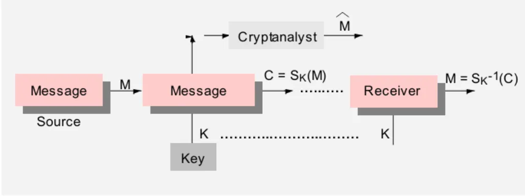
Chapter 2. Figure 2.1 Symmetric key cryptosystem...………. 30
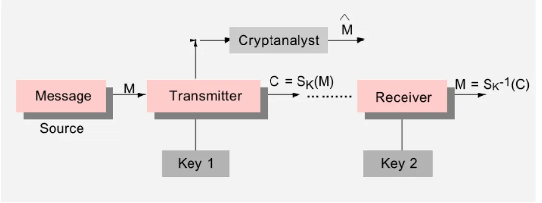
Figure 2.2 Public key cryptosystem...………... 31
Figure 2.3 ElGamal protocol representation...………. 32
Figure 2.4 Diffie-Hellman Scheme...………... 34
Chapter 3. Figure 3.1. CSA Unit……… 50
Figure 3.2. Block Diagram of the CSA technique……… 50
Figure 3.3 CSA trees for 3,4, and 5 operands……….. 51
Figure 3.4 Modular exponentiation description...………. 51
Figure 3.5 Modular Multiplier Datapath Architecture...……….……... 52
Figure 3.6 Modular Multiplier Hardware System...………. 53
Figure 3.7 Modular architecture of the multiplier………….……….. 54
Figure 3.8 Basic cell (a) Schematic capture (b) Connectivity...……… 55
Figure 3.9 Timing diagram………...………... 56
Figure 3.10 A tree structure for calculating C16…………...………. 58
Figure 3.11 Bit slices………...………. 59
Figure 3.12 12x12 bits modular multiplier layout...……… 59
Figure 3.13 Control Unit………. 60
Figure 3.14 Simulation results...……….…… 61
Figure 3.15 Test chip microphoto…...……… 62
Figure 3.16 Functional testing results…...……… 62
Figure 3.17 Test screen photos…...……… 66
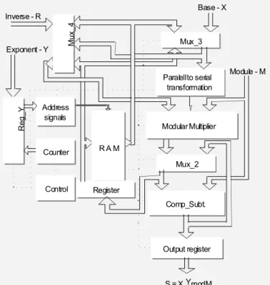
Chapter 4. Figure 4.1 Block diagram of the modular exponentiation operator...……… 78
Figure 4.3 Modular Exponentiation System Block Diagram……...……….………. 86
Figure 4.4 Exponent Register………...……….……….88
Figure 4.5 Schematic Capture of the System....………..…….………. 89
Figure 4.6 Multiplier and Parallel to Serial Unit.………....……….……….90
Figure 4.7 Modular Multiplier Diagram………90
Figure 4.8 Parallel to Serial Unit………...……….……….91
Figure 4.9 Parallel to Serial Conversion………...……….………. 91
Figure 4.10 Exponent Register, control part and intermediary memory....……….92
Figure 4.11 Schematic illustrating main control signals…………...……….………. 93
Figure 4.12 Schematic of (a) Control_sig and (b) Pro_Count_Y....……….……..…. 94
Figure 4.13 Schematic of (a) Prog_Count_10 and (b) Prog_Count_6....……….……. 95
Figure 4.14 Registers array………...……….………. 95
Figure 4.15 Multiplier Subtractor Loop………...……….………. 96
Figure 4.16 (a) CLU scheme (b) 32-bits Carry Look Ahead subtractor....…………. 97
Figure 4.17 Schematic of 32-bits CLA subtractor....……….………..…. 98
Figure 4.18 Overflow detection and Subtraction operation………....……….……..…. 99
Figure 4.19 Modular Exponentiation simulation results…………....……….……..…. 102
Figure 4.20 Modular Exponentiation simulation results…………....……….……..…. 103
Figure 4.21 (a) Automatic placement (b) Final Layout………....……….………. 103
Figure 4.22 Core of the Cryptosystem Layout………....……….………….……. 104
Chapter 5 Figure 5.1 Energy band structures of silicon and GaAs...………. 117
Figure 5.2 Carrier mobility in GaAs and Silicon...………... 118
Figure 5.3 Steady state electron in GaAs and Silicon ...………. 118
Figure 5.4 Steady state electron in GaAs and Silicon ...………. 118
Figure 5.5 Improvements in GaAs MESFET reliability compared to silicon....……...121
Figure 5.6 SBFL three input NOR………...……... 124
Figure 5.7 SCFL Logic Structure………...……... 124
Figure 5.8 PRL schematic………...……... 125
Figure 5.9 PCFL schematic………...……... 125
Figure 5.10 DPTL schematic………....……...125
Figure 5.11 Two TDFL inverters………...……... 125
Figure 5.12 TTDL schematic………...……... 126
Figure 5.13 SPDL schematic………...……... 126
Figure 5.14 GaAs MESFET structure of Vitesse technology...…………... 130
Chapter 6.
Figure 6.1 Conventional memory cell limitations...………. 142
Figure 6.2 New cell diagram...………. 144
Figure 6.3 Pull-up delay and current dissipation for different W ratios....………148
Figure 6.4 Noise margin...……… 149
Figure 6.5 Block diagram...………... 151
Figure 6.6 PRL sense amplifier...………. 152
Figure 6.7 1 Kbit layout...………. 153
Figure 6.8 Write and read operations - Wave form...………. 154
Figure 6.9 Fully pipelined read/write timing using slow parameters...………... 155
Figure 6.10 Worst case operating conditions……….. 156
Figure 6.11 Test chip microphoto...……...…………... 156
Figure 6.12 Functional testing results...……….. 157
Figure 6.13 Sense amplifier outputs...……… 158
Chapter 7. Figure 7.1 DC2FL Structure...………... 167
Figure 7.2 Variation of charging delay versus current consumption...………… 168
Figure 7.3 Output stage schematic ...………... 169
Figure 7.4 DC2FL inverter dc transfer curve...……….……... 170
Figure 7.5 Power dissipation graph...……….. 172
Figure 7.6 Test chip layout...……….. 173
Figure 7.7 Current consumption at different power supply voltage………. 174
Figure 7.8 Current consumption waveform……….. 174
Figure 7.9 Schematic of a EMDL gate...……….. 175
Figure 7.10 Delay and power consumption versus enable voltage level...………... 177
Figure 7.11 Transient HSPICE simulation...……….. 178
Figure 7.12 The 8-bits RCA...………... 181
Figure 7.13 EMDL and DCVS Static currents...………... 182
III. List of tables
Chapter 1.
Table I. Market of GaAs devices from 1991 to 2000...……… 8
Table II. Low Power Hierarchical Design………..11
Chapter 2. Table I Periodicity example for some module...………… 26
Table II Periods and half periods...………….. 26
Table III Parameters of RNS with small ai and Per(Mi)...………… 28
Table IV Factoring n difficulty...……….….………. 29
Table V. Factoring for each length of n ...………… 29
Table VI. Public-key techniques………. 37
Table VII. Cryptography techniques features……….. 37
Chapter 3. Table I Techniques for speeding up the calculation...…………... 42
Table II Hardware implementation of modular multiplication...………… 48
Table III Number of levels θ(r) in function of r...……….. 51
Table IV Power consumption of the control part...……… 63
Table V Power consumption of the operative part...………. 63
Table VI Global power consumption…………...……… 64
Table VII Architecture performance………...……… 67
Chapter 4. Table I Features of some modular exponentiation algorithms...…….. 76
Table II A survey of Hardware implementations...……….. 77
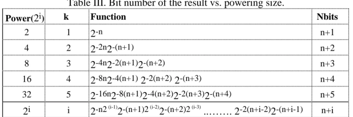
Table III Number of bits of the result vs. powering size...………. 82
Table IV Function for big word length ………...………. 82
Table V Corrective factors...………...………. 83
Table VI Cache size………...………...………. 84
Table VII Maximum number of multiplication...…...………. 87
Table X All multiplication……….…...……...………. 100
Table XI From j=2 to 2d -1…...……...………. 100
Table XII Exponent Register Fields…….…...……...………. 100
Table XIII Decimal and Modular Products…...……...………. 101
Table XIV Architecture performance …...………... 105
Table XV State of the art of the cryptosystems .…...……….. 105
Table XVI Technical characteristics of some Smart Cards systems………. 106
Table XVII Comparisons of computation times………. 107
Chapter 5. Table I. GaAs / Silicon Electrical Properties...………... 116
Table II Barrier height in volts for various types of semiconductors...………. 119
Table III Circuit requirements for Very High Speed and Low Power ICs…………. 127
Table IV European GaAs Foundries - World Wide merchant market...………....129
Table V. MESFET model parameters……….130
Chapter 6. Table I MESFET model parameters...……….. 152
Table II Memory cell performance...………... 153
Table III Memory cells comparison...………... 153
Table IV Core current consumption...………... 157
Table V Control part current consumption...………. 157
Chapter 7. Table I. Full Adder Simulation results...……… 171
Table II Latched full adder simulation results...…….……… 171
Table III 8-bit ripple carry adder simulation results...….………. 172
Table IV Test patterns set……….. 173
Table V Current consumption………173
Table VI Full adder HSPICE simulation results...……… 180
1. Introduction.
1 . 1 . Cryptography.
In the electronic age, information exchange that could benefit persons or groups can also be used against such groups or individual persons. Industrial espionage among highly competitive businesses often requires that extensive security measures be put into place. And, those who wish to exercise their personal freedom may also wish to encrypt certain information. Cryptography is the art or science of secret writing, or more exactly, of storing information, is the art of encoding data in a way that only the intended recipient can decode it, and know that the message is authentic and unchanged.
There are many reasons for using encryption techniques. Different applications that require privacy, trust and access control, like electronic money, secure communications, passwords, and many others, should all use strong encryption methods when possible.
A cryptosystem is a method to accomplish that. The ideal cryptosystem would be an applied specific system for one particular purpose, which would satisfy the requirements of security, reliability and ease-of-use : reliability means that the cryptosystem, when used as its designer intended it to be used, will always reveal exactly the information hidden when it is needed. Security means that the cryptosystem will in fact keep the information hidden for all those persons intended to crack the system. Cryptanalysis is the practice of defeating such attempts to hide information. Cryptology includes both cryptography and Cryptanalysis.
The security of a cryptosystem is always relative to the difficulty of breaking a secret message and the conditions under which it will be used.
In general, the security of a cryptosystem can only be measured by its resistance to actual attempts to break it in practice. Those that have resisted the attentions of many cryptanalysts for many years may be deemed secure, at least until better methods of Cryptanalysis are invented.
1.1.1. Practical Cryptosystems.
Still, the methods of data encryption and decryption are relatively straightforward, and easily mastered. A cryptosystem is designed considering that decryption can be accomplished only under certain conditions, which generally means, only by persons in possession of both a decryption engine and a particular piece of information called the decryption key, which is supplied to the decryption engine in the process of decryption. All modern algorithms use a key to control the encryption and decryption. The message can only be decrypted if the key matches with the key used to encrypt it. The key used for decryption can be different from the key used in encryption, and this divides the algorithms in symmetric (or secret-key) and asymmetric (or
public-key) classes.
Symmetric algorithms, also called secret-key algorithms, use the same key for both encryption
and decryption. The key is not to be leaked to outside enemies, should be changed often and be sufficiently random. Different symmetric algorithms use different length keys, usually a longer key means higher security. Symmetric algorithms are generally faster than asymmetric ones and use a much shorter key.
Public key systems were developed in the 1970s to solve the problem of secure key exchange.
In this system the decryption key is not the same as the encryption key. Such public key systems can, if used properly, go a long way toward solving the problem of secure key exchange because the encryption key can be given out to the world without compromising the security of communication, provided that the decryption key is kept secret.
Although public key cryptography in theory solves the problem of secure key exchange, it does in general have a couple of disadvantages compared to symmetric (or secret) key systems. The first is speed. Generally public key systems, such as PGP, are much slower than secret key systems, and so may be suitable for encrypting small amounts of data. The second disadvantage of public key systems is that there is a problem of key validation.
There are numerous public key cryptosystems, the most well known being the one based on the RSA. Messages ciphering and digital signature are two of the most extended cryptography applications.
The idea behind public key encryption messages ciphering, is that it is computationally infeasible to calculate the secret key from the public key and that no information can be obtained about the secret key from any message by knowing the public key.
Digital signatures are a way of signing data in the same way that we sign documents today.
signed the message; the signature is an integral part of the message and cannot be transferred to another message; the signed message cannot be changed in any way without being detected; the signer cannot deny signing a message after doing so.
In some cases it is possible to show that cracking a cryptosystem is equivalent to solving some particular mathematical problem. Most implementations of public key cryptography rely on the hard problems of factoring large numbers, it means numbers with several hundred decimal. Whereas it is relatively easy to multiply two large primes, it is currently very difficult to factor the result back to the two original primes. In the case of RSA algorithm, it is widely believed that these are secure if and only if the problem of factoring large numbers is insoluble, that is, computationally infeasible in real time.
There are few operations in mathematics that are truly 'irreversible'. In the case of the RSA encryption algorithm, it uses very large prime numbers to generate the public key and the private key. Although it would be possible to factor out the public key to get the private key, the numbers are so large as to make it very impractical to do.
Modern cryptographic algorithms are meant to be executed by computers or specialised hardware devices for which there are several different cryptographic algorithms and methods which rely for its security on the difficulty of factoring large numbers. Traditionally, several methods can be used to encrypt data streams, all of which can easily be implemented through software, but not so easily decrypted when either the original or its encrypted data stream are unavailable.
Although several methods are developed to be implemented through software, some algorithms and protocols have been oriented to hardware implementation, more specifically, to smart cards applications. As known, smart cards market is each time more important. The U.S. market has lagged behind Europe and Asia in using smart cards. The companies concluded that several factors must be combined to push smart cards successfully into the U.S. market. They included greater interoperability and the ability to use the chip cards for unattended needs such as telephones, parking meters, and transit systems. The smart card is currently used mostly in Europe where it is used as a pay phone calling card or for vending machines. The United States is beginning to see smart cards in use for GSM phones, laundry, and vending applications.
Smart cards are plastic cards with a credit card size, that have an embedded computer chip. The card companies are eager to move to smart cards from today's standard magnetic stripes on the back of cards so that more data or applications can be loaded onto cards. Multifunction cards include more than one use, for example, loyalty or frequent-user programs on the same card
a magnetic tape similar to how a computer writes information onto a floppy disk. This method, though powerful, has proved to be insecure in many instances.
Magnetic cards are easy to reproduce and many use no form of encryption on their identifier. The smart card achieves this because the card has a small yet powerful computer built into it. This computer allows the card to interact with the card reader, not just pass information to it. Just as there are many different uses for a smart card there are many different flavours of smart cards not to be confused with optical memory cards.
One of the key benefits of smart cards is the ability for some cards to support on board cryptography. Cryptographic smart cards open up a whole new realm in information security because it now allows a secure place for storing of keys and key rings. By doing the actual cryptography on the card, the keys never have to leave their storage place. This gives the card holder a secure way of storing keys especially if the key pair was generated on the card. Smart cards performing cryptographic functions can be utilised in applications such as key and certificate verification, encryption, and random number generation between others.
Although the uses for smart cards are numerous, there is still the cost issue. Magnetic stripe cards cost as little as 6 - 8 cents to be made, whereas a smart card can cost up to 10 to 15 times that cost. For this reason, small size architectures without degradation of performance is very attractive for this specific application. Modular exponentiation is the operation most widely used in many protocols and algorithms. The design of the chip for performing modular exponentiation based on regular and small architectures would allow to implement this function on smart cards.
Considering that several cryptographic applications require high performance systems, low power strategies applied to high speed technologies as GaAs must be considered.
1.2. Gallium Arsenide Technology.
Nevertheless, the world-wide semiconductor market in 1996 down 6.2 percent from 1995’s, this market is still growing and will surpass the $ 300 billion of dollars point in the year 2001. Semiconductor market analyst explain that the drop was due in large part to the bottom falling out of the DRAM market in late 1995 and throughout 1996. In 1996, the world-wide semiconductor market achieved at $ 141.7 billion of dollars. European semiconductor market consumption revenue achieved at $ 28.5 billion and is expected to grow to $ 62.1 billions by the year 2001. As can be seen from the Figure 1.1, where both revenue forecast and revenue by product are presented, the expectations of growth are attractive.
0 50 100 150 200 250 300 350 Billions of dollars 1996 1997 1998 1999 2000 2001 Microcomponents Memory Other Logic Discrete Analog Opto 24% 26% 14% 13% 8% 3% 12%
(a) Revenues forecast. (b) Revenue by product.
Figure 1.1. World-wide semiconductor market. [1]
Silicon MOS technology has been the main medium for computer and system applications for a long time and this technology will continue to fill this role. However, in Silicon MOS technology several limitations are already becoming apparent in state-of-the-art fast digital systems [2], due to the fact that, system level requirements quickly surpassed the performance that silicon was able to deliver. Since a few years, in order to overcome these limitations some developments in silicon technology have been achieved.
However, with the development of communications and more specifically portable telecommunication and multimedia systems which require high clock frequency, logic families as BiCMOS, GaAs and SiGe are becoming more attractive to those types of applications. For that reason, some parallel significant advances are also beginning to take place with Gallium Arsenide technologies.
Gallium Arsenide (GaAs) MESFETs became an enabling technology that allows overcome the silicon limitations in ultra high speed applications. This technology has evolved and changed over the last 30 years and has finally found its marketplace into the semiconductor's industry. Nevertheless, some efforts are currently done in order to develop other technologies, GaAs technology continues to play an important role in communication applications, such as: compact cell phones, high frequency wireless base stations and global positioning systems (GPS) [3].
Gallium Arsenide’s resurgence also stems from an ever-expanding profusion of applications, such as medical [4], analogue cellular/PCS handsets, digital cordless handsets, wireless local loop [5], wide band CDMA, automotive [6] and radar communication (IMT 2000 system). Analogue and discrete GaAs semiconductors continue to be a very important segment in digital
communications system because of the peak power, supply voltage and signal distortion requirement.
Since a few years, digital GaAs applications have emerged in the form of one company which has become the market leader: Vitesse Semiconductor. Vitesse has managed important growth in an area in which digital GaAs is again an enabling technology. The company, whose process technology is said to address the high-speed needs of telecom and datacom, reported in the third quarter of 1998 revenue of 46.1 millions of dollars, up 67% from last year and up 15% from second quarter of 1998 [7].
Currently, the use of compilers for digital GaAs IC design using Vitesse technology is available [8]. Another data-path compiler for the public domain ALLIANCE CAD System has been also developed [9].
The market for GaAs beginning 1997, started growing at 50% to 60% a year [10]. Digital GaAs market reached over $1 billion in 1996. On the other hand, the GaAs wafer industry is expected 8 MSI (million square inches) by the year 2000. Revenue is expected to increase from $ 153 million in 1996 to over $ 400 million in 2000 [1].
The perceived European GaAs IC market from 1984 to 1994 is shown in figure 1.2. The leading sector until the late 1980’s was analogue MMIC, but that both digital and optoelectronic ICs will be employed increasingly in systems. The market for digital GaAS integrated circuits in Europe increased from US $ 58.8 M in 1989 to US $ 1.088 B in 1994.
1984 - US $ 3 M 100% Analogue 1989 - US $ 140 M 42% Digital 2% Opto-electronic 42% Analogue 1994 - US $ 1.876 B 58% Digital 28% Analogue 14% Opto-electronic
Top four U.S. producers: Anadigics, TriQuint, Vitesse, Motorola and their homologous Japanese are the main GaAs ICs industries, corning the GaAs IC world market. In 1992, the top seven European producers of GaAs devices: Alenia, Alcatel, Daimler-Benz, GEC Marconi Materials Technology, Philips Microwave Limeil, Siemens and Thomsom-CSF created into the Eureka Program the EuroGaAs initiative which was oriented to penetrate the GaAs ICs world market.
In 1995, the European GaAs ICs production represented only 24% of the global market but its sales achieved hardly 10% of world market. The evolution of the captive market for GaAs ICs is shown in table I. As can be seen, the market is growing very fast. Specifically for digital GaAs ICs the market will be increased from 71 millions of dollars in 1991 to 681 millions of dollars in 2000.
Table I. Market of GaAs devices from 1991 to 2000 [12].
Millon of dollars 1991 1996 2000
Digital ICs GaAs 7 1 324 681
MMIC GaAs 104 289 643
Discrete GaAs 176 237 341
Total 351 850 1665
However, having discussed the potential of GaAs technology, the performance of GaAs integrated circuits with reasonable complexity must be also considered. GaAs complex systems perform better in terms of propagation delay but not in terms of power dissipation. Power consumption has become a critical concern in both high performance and portable applications.
Over the past years, much effort has been directed towards increasing the speed of digital integrated circuits and decreasing the area size. Only in recent times the power consumption of these circuits has been considered as a third constraint during their development. Currently, the researching in high speed VLSI design has been shifted from high speed to low power emphasis due to the proliferation and rapidly growing range of portable electronic systems containing microelectronic devices [13]. This factor has forced a new definition of priorities and considerations of design.
1.2.1. Low Power GaAs Circuits.
Because of GaAs technology requires also very low power dissipation a large effort has been spent in the development of both efficient low-power GaAs technologies [14], [15] and high speed low power GaAs logic styles [16], [17] which should allow the extension of this attractive technology to high speed low power applications.
have been published obtaining a reduction in active global power dissipation. In each case, the speed-power product has been improved.
Methods for solving the power dissipation drawbacks in GaAs technologies are being strongly studied. The high electronic mobility and low knee voltages of GaAs are ideal for low supply voltage operations [25]. Low voltage operation has already been one of the most important design issues for GaAs circuitry not only to further reduce power dissipation , but also to ensure reliability for devices. In parallel, some important progress in power reduction, performance and temperature tolerance in several GaAs complex systems have been obtained.
So, Low Power GaAs LSI technology is an attractive researching field in which considerable attention is being focused. Because this is an important and growing area of electronics, in 1995, Motorola has developed a self aligned complementary GaAs technology for Low-Power, high speed digital and mixed mode applications. The complementary GaAs (CGaAs) shows a speed power performance of 0.01µW/MHz/gate at 0.9V in digital circuits [14].
All mentioned and recent exploratory achievements in the movement towards low power operation seemingly give promise of future improvements. This new researching field promises to satisfy the speed requirements of present day computers and indeed the super computers. Low Power Gallium Arsenide technology will not displace silicon but may be used in conjunction with silicon to satisfy the need for Ultra High Speed Integrated Circuits (UHSI).
The early years of mobile communication were based on first generation analogue systems, such as NMT/TACS/AMPS, the development of which were regionally based in Europe and the USA. However, worlwide there is a steady migration underway towards second generation digital systems, driven largely by the need for increased capacity.
In Europe the migration to digital technology is based on the GSM standard which was launched in 1992 and was rapidly adopted in Africa, the Middle East and the Asia Pacific Region. DCS 1800 system is based on the same protocol as GSM but at twice the carrier frequency. In the USA the move to second generation digital systems started using one of the two competitive digital standards: TDMA (Time Division Multiple Access) or CDMA (Code Division Multiple Access).
The different services to be offered following introduction of any digital communication system included: short message service, calling line identification, conference calls, high speed data and others. Additionally, there are some extra benefits such as encryption and the ability to provide a portfolio of data related services based on digital technology [26]. VLSI circuits that accelerate the encryption and decryption of messages using the RSA encryption technique and circuits capable of performing long word length modulo multiplication at very high speed attract much
interest for cryptography applications. For that reason, designer who research to accelerate RSA cryptographic processing are looking the high speed advantages of Gallium Arsenide VLSI technology as an interesting alternative.
1.3. Objectives
Cryptographic methods such as encryption and decryption process and other secret communication problems require the exponentiation arithmetic function to hidden information. Exponentiation arithmetic function is executed as repetitive multiplication leading to the long word length modulo multiplication operation to be the main and more frequently function to be performed. Arithmetic operators exhibit in general a great activity and dissipate consequently a significant share of the power supplied to a circuit. That is specifically true for a multiplier which dissipates much more power than an adder when activated due to the fact that its design or layout structure is not as regular as an adder.
Considering that, the ultimate performance of an integrated circuit can be substantially improved by using a full customised macro cells library for its design (being that particularly true for GaAs circuits where speed performance is critical, the cost of real estate is high, and design expertise is scarce), the goal of this work is focused on developing an alternative architecture (in CMOS technology) for executing modular exponentiation which must satisfy the requirements of speed, power consumption and size for smart card implementation.
Also, low power design GaAs strategies to be used in arithmetic macro blocks implementation are considered. These structures are conceived to be applied in an eventual Low Power GaAs Cryptosystem using the same architecture. Up to now there is no arithmetic macro blocks to complete the development of Low Power GaAs VLSI cryptosystems. Typical delay, average power consumption and area for each function are the principal features to be characterised. Compacts and high speed designs combined with new low power strategies which take advantage of superior performance of GaAs are proposed looking predominantly the power reduction constraint as a principal goal. In order to minimise the power of these ICs, different low power methodologies are applied at different abstraction levels of the system design.
Two specific performance parameters which must be improved are consumption and operating voltage. A reduction in current consumption and operating voltage allows to obtain a significant reduction of power dissipation. The significance of improvement in these two parameters is the main motivation.
considering low power strategies, in order to verify the power reduction that can be achieved. In order to minimise the power of these ICs, different low power methodologies will be applied at different abstraction levels of the system design. So, in table II, are shown the five distinct levels where optimisation techniques must be implemented.
Table II. Low Power Hierarchical Design. System design
Algorithms
Architecture design Circuit design Process technology
This work will contain 7 chapters. Chapter 2 presents an introduction of cryptography and modular notation concepts which will be used along this work. Chapter 3 shows an alternative architecture for executing modular multiplication, as well as, simulation and experimental results of the prototypes.
Chapter 4, presents the conceived architecture for calculating modular exponentiation which is based on multiplier proposed architecture; performance and simulations are discussed. Those chapters describe in general the internal architecture used to compute modular exponentiation which is the core operator of the cryptosystem. It could be also used to implement the core of a Low power GaAs cryptosystem.
Chapter 5 discusses some important characteristics of GaAs technology and comparison on silicon, the general concepts which will be used for implementing a low power GaAs functions as well as the low power techniques used in each design.
Cache-memory play an important role in the overall power-efficiency of a cryptographic system, since it can reduce the data traffic between the arithmetic operator and external memory. For this reason, we study in chapter 6 a novel Low Power GaAs memory cell. So, as on-chip memory accesses consume significantly less energy than accesses to off-chip memory, this cell is appropriated to implement cache high speed memories. Chapter 7 analyses two asynchronous structures to design low power GaAs arithmetic circuitry. Both approaches were verified through two full custom eight bits ripple carry adders obtaining significant power consumption reduction.
The low power functions will be designed with Vitesse III technology (0.6 µm - GaAs) using the design kit of Vitesse on Cadence environment. All experimental measures were done at CIME Test Department. The test chips were fabricated through CMP Service. Part of the research was supported by GARDEN (Galium Arsenide Reliable Design Environment) ESPRIT project CT93-0385.
1.4. References
[1] E.J. Lum, "GaAs semiconductors: New market opportunities and emerging applications trends.", Invited paper, Proc. IEEE 5th European Gallium Arsenide and related III-V compounds Applications Symposium, Bologna, Italy, Sept., 1997.
[2] K. Eshraghian, "Gallium Arsenide Integrated Circuits Design", Internal Report, Electronics Laboratory of the Swiss Federal Institute of Technology, Lausanne, Switzerland, April, 1989.
[3] E. Fishkill, IBM Eyes Merchant Packaging Services, Hebdo, Electronic Engineering Times, N.Y., July 13, 1998.
[4] K. Carr, “Use of Gallium Arsenide in Medical Applications”, IEEE GaAs IC Symposium, USA, 1995.
[5] M. Mitama, "Mobile Communications Systems Trend in Japan and Device Requirements", IEEE GaAs IC Symposium, USA, 1995.
[6] A. Colquhoun, H. Meinel, “Automotive Applications of GaAs Components”, Proc. IEEE European Gallium Arsenide and related III-V Compounds Applications Symposium, Paris, France, 1996.
[7] Margaret Quan, Motorola, AMD Post Losses, Hebdo, Electronic Engineering Times, Finance, pps. 78-79, July 13, 1998.
[8] R. Oettel, “The use of Compilers for Digital IC Design”, IEEE Gallium Arsenide IC Symposium, USA, 1993.
[9] O. Beaurin, A. Amara, “A GaAs Data-Path Compiler”, Proc. IEEE European Gallium Arsenide and related III-V Compounds Applications Symposium, Paris, France, 1996. [10] L. Armstrong, O. Port, S. Brull, “GaAs Guzzlers on the Info Highway ?, Science and
Technology, Business week , August 19, 1996.
[11] "Critical Design Issues for GaAs VLSI Circuits", Internal Report, Microelectronic Center, Middlesex University, London, UK, June, 1991.
[12] L. Stéphan, "L’Europe devient compétitive en circuits GaAs ", Hyper 97, Electronics International, Hebdo, No. 248, January, 1997.
[13] A.P. Chandrakasan, R.W. Brodersen, "Low Power Digital CMOS Design", Kluwer Academic Publishers, 1995.
[14] B. Bernhardt, M. LaMacchia, J. Abrokwah, J. Hallmark, R. Lucero, B. Mathes, B. Crawforth, D; Foster, K. Clauss, S. Emmert, T. Lien, E. Lopez, V. Mazzota, B. Oh, “Complementary GaAs (CGaAs): A high performance BiCMOS Alternative”, IEEE GaAs
[15] H. Fawaz, J.F. Thiery, N. Linh, F. Mollot, J. Pesant, M. Francois, M. Muller, E. Delos, G. Salmer, “III-V Complementary HIGFET technology for low power microwave and high speed/low power digital integrated circuits”, Proc. IEEE European Gallium Arsenide and related III-V Compounds Applications Symposium, Paris, France, 1996. [16] A. Chandna, R. Brown, D. Putti, C.D. Kibler, "Power Rail Logic: a Low Power Logic
Style for Digital GaAs Circuits. IEEE Journal of Solid-State Circuits. Vol.30, No.10, October, 1995.
[17] K.R. Nary, S. Long, "GaAs Two-Phase Dynamic FET Logic: A Low Power Logic Family for VLSI”, IEEE Journal of Solid-State Circuits. Vol.27, October, pp. 1364-71, 1992.
[18] R. Kanan, B. Hochet, M. Declerq, "Pseudo-Complementary FET Logic (PCFL): A Low Power Logic Family in GaAs”, IEEE Journal of Solid-State Circuits. Vol.31, No.7, July, 1996.
[19] P. Lassen, S. Long, K. Nary, "Ultra-Low Power GaAs MESFET MSI Circuits using Two-Phase Dynamic FET Logic”, IEEE Journal of Solid-State Circuits. Vol.28, No. 10, October, pp. 1038-45, 1993.
[20] V. Chandramouli, N. Michell, K. Smith, "A New, Precharged, Low-Power Logic Family for GaAs Circuits”, IEEE Journal of Solid-State Circuits. Vol.30, No. 2, February, pp. 140-43, 1995.
[21] D.H.K. Hoe, A.T. Salama, “Pipelining of GaAs Dynamic Logic Circuits”, Proc. IEEE International Symposium on Circuits and Systems, San Diego, USA, May, 1992.
[22] H. Kawasaki, "A Low Power 128x1-bit GaAs FIFO for ATM Packet Switcher” IEEE
Journal of Solid-State Circuits. Vol.31, No.10, October, 1996.
[23] R. Kanan, A. Guyot, B. Hochet, M. Declerq, "A Divided Decoder-Matrix (DDM) Structure and its Application to a 8Kb GaAs MESFET ROM", Proc. 30th IEEE ISCAS, Hong Kong, 1997.
[24] D. Abbott, K. Eshraghian, “SiGe versus GaAs - Is there a challenge ?”, Proc. IEEE European Gallium Arsenide and related III-V Compounds Applications Symposium, Paris, France, 1996.
[25] C. Huang, "GaAs ICs for 3 volt Electronic", Proc. of the IEEE 5th European Gallium Arsenide and related compounds Applications Symposium, Bologna, Italy, Sept., 1997. [26] K.M. Baughan, "The wireless Communication Market - Is there a Place for GaAs", IEEE
2. Modular Notation and Cryptography.
2.1. Introduction
Most of cryptography applications such as key public cryptosystems incorporate a exponentiation unit to implement algorithms for executing modular operations. The most widely used operations are addition, multiplication and exponentiation. The numbers to be operated are usually represented in modular representation. In this chapter we will briefly introduce the basic concepts of modular arithmetic as well as some general concepts of cryptography including some known protocols in order to familiarise oneself with a language.
The development of computer controlled communication networks promises effortless and inexpensive contact between people or computers on opposite sides of the world, replacing most mail and excursions with telecommunications. For many applications these contacts must be secure against both eavesdropping and the injection of illegitimate messages. Secret digital writing is being used to avoid message transformations. Techniques to avoid eavesdroppers actions are known as cryptography. The word comes from the Greek words kryptos (“hidden”) and graph (“writing”). The history of cryptography dates far back. The Spartans used the “scytale” method as early as 400 BC. Secret writing has been used by many ancient societies to protect information beyond typical methods.
Currently, cryptosystems are more frequently required in applications as remote cash dispensers, high speed computer terminals, authentication, digital signatures and private communication between others. In Europe, the new Smart Card Microcomputer Center will orient their principal applications to bank and telecommunications security, developing a cryptoprocessors family [1].
Due to the fact that, several of cryptography applications use satellite communication where principally radiation tolerant integrated circuits are needed, cryptography systems are also included into the market behaviour of GaAs digital integrated circuits which will be doubled in the next four year [2].
2.2 Concepts
Several concepts are used in cryptography. First of all, we will define the terms more frequently used, in order to manipulate a common language:
- Cryptography may be considered as the art and science of both keeping messages secure and reading messages meant to be secure. In other words, is the study of secret writing and is used to protect the exchange information between people or computers.
- Encryption (encode) and decryption (decode) are two inverse procedures always used in cryptography operations. The procedures allow to cipher or decipher a message to be transmitted through public channels.
- Cryptology is the study of encryption and decryption methods. Is the branch of the mathematics embodying the art and science of both keeping messages secure and reading messages to be secure.
- Cryptanalisys consist in breaking a single secret message. To recognise patterns in order to develop decryption algorithms, find general weakness in encryption algorithm.
In terms of security, two concepts are frequently used: unconditionally secure is a system which can resist any cryptanalytic attack and is based on the existence of meaningful solutions to a cryptogram. The another term is computationally secure which denotes a secure system due to the computational cost of cryptanalysis.
2.3 Applications
In cryptography, mathematical systems are studied in order to solve two security problems:
i. Privacy or secrecy requires that an intruder should not be able to determine the plain text corresponding to given cipher text and should not be able to reconstruct the key by examining cipher text for known plain text. In other words, to prevent the extraction of information by unauthorised parts (ciphering messages). The message must not be vulnerable to eavesdropping or alteration.
ii. Authentication requires that the sender can validate the source of message, that means that it was transmitted by a properly identified sender and is not a reply of a previously transmitted message. We can identify two aspects:
- Message authentication or integrity requires the ability to insure that a message was not modified accidentally or deliberately in transit, by replacement, insertion or deletion. It is used to prevent the unauthorised injection of messages into a public channel.
- User authentication service is used to verify that an individual is who he claims to be. Also is a protection against a sender of message later denying transmission. It is also known as non repudiation service or digital signature.
The security problems which must be solved by cryptography systems are the insecurity of the publics channels (eavesdropping, injection of illegitimate messages) and authentication (illegitimate messages, digital signatures).
Strong security levels are required in applications as: remote cash dispensers, computers terminals, image compression, access control, authentication, confidentiality protection, key exchange, digital signatures, distributed network security management, private communication and hybrid systems.
2.4. Mathematical basis.
The mathematical fundament of the modern cryptography are functions of difficult inversion like as one-way functions, trap-door one-way functions, hash functions and one-way hash functions.
2.4.1 One-way functions
The one-way functions are easy to compute but difficult to invert. So, given some variable x and a one-way function f, is easy to compute f(x), but given f and f(x) is difficult to compute x. However, there is no proof that one-way functions exist. Mathematical discoveries are showing that more and more functions considered initially as one-way, are no longer so.
2.4.2 Trap-door one-way functions
Trap-door one-way functions are a subset of one-way functions. For these functions, giving a secret piece of information makes easy to compute the inverse of the function.
2.4.3. Hash functions.
Hash functions are usually many-to-one functions. They are used to characterise a larger piece of data. A Hash function accepts a variable-size message X as input and outputs a fixed-size representation H(X) of X, sometimes called a message digest. In general H(X) will be much smaller than X. H(X) might be 64 or 128 bits, whereas X might be a megabyte or more. 2.4.4. One-way hash functions.
These type of functions are both one-way and hash functions as explained below. They are also known as compression function, cryptographic checksum, manipulation detection code, message authentication code, data integrity check or contraction functions.
The one-way hash function has the additional property that given a hash value y, it is difficult to find a value x such that f(x) = y. There are also hash functions that require a key. Given k and x, you can compute y, but having any other combination of data does not provide enough information to easily compute any other data. Additionally, one-way hash functions used in cryptography are random. Each change in any bit of the input, changes in average half of the bits in the output. For this reason, one-way hash functions can serve to detect modification of a message, that is to say, it can serve as a cryptographic checksum.
One-way hash function presents as input a string of arbitrary length and its output is a unique fixed length number. Example MD5 produces 128-bits hash value. One way property consists in making computationally infeasible to find two documents with same hash. The properties of one-way hash functions can be summarised as:
- f can be applied to an argument of any size. - f produces a fixed-size output.
- f(x) is relatively easy to compute for any given x.
- For any given y, it is computationally infeasible to find x with f(x) = y
- For any fixed x, it is computationally infeasible to find x’≠x with f(x)’ = f(x).
The security of public key systems depends on the fact that the public transformations are trapdoor one-way functions. Trapdoors permit decoding by recipients. The modular arithmetic facilitates the wrapping concept. In next section the principal terminology and basically theory of modular arithmetic will be discussed.
2.5.1. Introduction
In normal arithmetic, operations like adding or multiplication present usually an important increasing output natures for each increasing input pattern set. This is not necessarily true in modular arithmetic. Modular arithmetic is an interesting and viable alternative for doing arithmetic on large integer numbers.
This “other” arithmetic is based on some simple principles of number theory. It is possible to represent any integer number X , using several module m1, m2, m3, . . . , mh, that contain not common factors:
x1 = X mod m1, x2 = X mod m2,
. . xh = X mod mh
Now, having the complete modular representation, it is possible to operate indirectly with “residues” obtained: X mod m1, X mod m2, ...,X mod mh, instead of directly with the number X. It is easy to compute (x1, x2, x3, ..., xh ) from an integer number X, without lost of information in this process. If xi equals the remainder of X divided by mi, then modular arithmetic expresses this as: Xmodmi = xi and is read “X modulo mi equals xi” [3] or can also be expresses as X ≡ ximodmi, and is read “X is congruent to xi modulo mi” Additionally the notation X≡Y mod M means that M divides X - Y that is X and Y lie in the same residue class modulo. ModM denotes a number Y such that X≡Y mod M.
2.5.2. Modular arithmetic operations.
Modular arithmetic can be added, subtracted, multiplied and exponentiated, the equivalent of repeated multiplication. Modular arithmetic satisfies the following properties for all residues α obtained from a division by an integer M expressed in radix r, that remainders form what is called the ring of residues modulo M.
i. (α + 0) = (0 + α) = 0 (3)
ii. α + (M - α) = 0 (M - α is the additive inverse of α ) (4) iii. α.1 = 1. α = α
(5)
vi. (x + y) mod M = ((x mod M) + (y mod M)) mod M (8) vii. (x - y) mod M = ((x mod M) - (y mod M)) mod M (9)
viii. (x
.
y) mod M = ((x mod M).
(y mod M)) mod M (10)ix. (x exp y) mod M = ((x exp (y-r) mod M)
.
(x exp r mod M)) mod M (11)From mentioned properties we have:
- If XYmod M = R then (XS)Ymod(MS)div S = R (12) - X R-1 + Y R-1≡ S R-1mod M if and only if X + Y ≡ S mod M (13)
One can not divide congruencies in all cases. Another interesting and remarkable property consists in that for any pair of relatively prime integers, multiples of each can always be found such that their difference is unity. In other words, there always exists some multiple of an integer p which leaves a remainder of one when divided by another integer prime to it. The multiplier of p is always a smaller number than the divisor of the product.
x. (a
.
x) - (b.
y) = 1 (14)This property brings us to the inverse modulo function which is equivalent to finding a number such that:
xi. (y
.
x)modM = 1 or y.
x ≡ 1modM (15)For cryptographic applications, we want M to be as large as possible, it is easiest to let m1 be the largest odd number, and to let m2 be the largest odd number minor than m1 that is relatively prime to m1.
2.5.3. Underlying functions
2.5.3.1. Euler and Fermat totient function
Also known as only Euler totient function or Euler Φ function. Euler and Fermat identity are considered as a way to choose the large random numbers m1 and m2. For any integer message X which is relatively prime to M, it means, gcd(X, M) = 1 then XΦ(M)modM = 1. Let Φ(M) be the Euler totient function giving the number of positive integers smaller than M which are relatively prime to M. Unlike Fermat’s little theorem, M does not have to be prime. For this reason Euler totient function is refereed to as Euler’s generalisation of Fermat’s little theorem. The Euler totient function presents the following properties for any integer (message) X:
i. Euler totient function is multiplicative, so, if Φ(m1)=x and Φ(m2)=y, then Φ(m1m2) = xy. ii. If m1 is prime, then Φ(m1) = m1-1, since all numbers smaller than a prime are not divisors of
prime.
iii. Then, if M = m1m2, where m1 and m2 are primes we can write Φ(M) = Φ(m1)Φ(m2) and
Φ(M) = Φ(m1-1)Φ(m2-1), so, Φ(M) = M - (m1 + m2) + 1.
So, if we choose a given number d which is relatively prime to Φ(M), it has a multiplicative inverse e in the ring of integers modulo Φ(M). It is denoted as e.d ≡ 1modΦ(M). Euclid's
algorithm allows to calculate that.
2.5.3.2. Euclid’s Algorithm.
The Euclid's algorithm [4], is very useful in modular arithmetic and basically is used to calculate the greatest common divider (gcd) of two integer numbers r0 and r1, allowing also to compute the inverse multiplicative of a number. The algorithm is shown below:
r0 = q1r1 + r2 0 < r2 < r1 r1 = q2r2 + r3 0 < r3 < r2 r2 = q3r3 + r4 0 < r4 < r3 . . rm-2 = qm-1rm-1 + rm 0 < rm < rm-1 rm-1 = qmrm gcd (r0, r1) = gcd (r1, r2) = gcd (r2, r3) =... = gcd (rm-2, rm-1) = gcd (rm-1, rm) = rm Then gcd (r0, r1) = rm
Euclid’s algorithm can be used to determine if a positive integer b < M, has its module M inverse multiplicative, that is ∃τ such that τ.bmodM = 1. Replacing r0 = M and r1 = b it is possible to know the existence of the inverse multiplicative.
Theorem: Let t0,t1,...tm .be a sequence of recurrences:
t0 = 0 t1 = 1
. .
tj = tj-2 - qj-1tj-1mod r0 if j ≥ 2.
By mathematical induction procedure we assume that is true for j = 0 and j = 1 and then we proof that is true for j = i - 1 and j = i - 2, i ≥ 2.
ri - 2 ≡ ti - 2 r1 mod r0 ri - 1 ≡ ti - 1 r1 mod r0 Then we have: ri = ri - 2 - qi - 1ri - 1 ri ≡ ti - 2 r1 - qi - 1ti - 1r1 (mod r0) ri ≡ (ti - 2 - qi - 1ti - 1) r1 mod r0 ri ≡ ti r1 mod r0
As a corollary of the last theorem we have that: if gcd (r0, r1) = 1, then tm = r1-1 mod r0
The inverse modulo function is that number which multiplied by the original number gives one as the remainder x ≡ y-1 modn. If y and n are relatively primes then x = y-1modn has a unique solution, on the contrary if y and n are not relatively primes the equation has not solution. If n is a prime number, then every number from 1 to n-1 is relatively prime to n and has exactly one inverse in that range. The Euclid’s algorithm which is used to find the inverse multiplicative in modular representation can be expressed as:
n0 <--- n b0 <--- b t0 <--- 0 t <--- 1 q <--- n0 / b0 r <--- n0 - q x b0 While r > 0 do temp <---- t0 - q x t
If temp ≥ 0 do temp <---- temp mod n
If temp ≤ 0 do temp <---- n - ((-temp) mod n) t0 <--- t t <--- temp n0 <--- b0 b0 <--- r q <--- n0 / b0 r <--- n0 - q x b0
If b0 ≠1 then the inverse multiplicative of b does not exist If b0 =1 then b-1 mod n = t
2.5.3.3. Fermat theorem
For any number x, which is not divisible by its exponent p, which is a prime number, in general we have that: if xp - x = y then y is divisible by p.