MÉMOIRE PRÉSENTÉ À
L'UNIVERSITÉ DU QUÉBEC À TROIS-RIVIÈRES
COMME EXIGENCE PARTIELLE DE LAMAÎTRISE EN GÉNIE ÉLECTRIQUE
PAR
BAHMAN GHOLAMI
APPLICATION DES SYSTÈMES DE CALCUL À HAUTE PERFORMANCE DANS LES ÉTUDES ÉLECTROTHERMIQUES À L'ÉCHELLE NANOSCOPIQUE
Université du Québec à Trois-Rivières
Service de la bibliothèque
Avertissement
L’auteur de ce mémoire ou de cette thèse a autorisé l’Université du Québec
à Trois-Rivières à diffuser, à des fins non lucratives, une copie de son
mémoire ou de sa thèse.
Cette diffusion n’entraîne pas une renonciation de la part de l’auteur à ses
droits de propriété intellectuelle, incluant le droit d’auteur, sur ce mémoire
ou cette thèse. Notamment, la reproduction ou la publication de la totalité
ou d’une partie importante de ce mémoire ou de cette thèse requiert son
autorisation.
La miniaturisation des MOSFETs a été le carburant de l'industrie semi-conducteur pour quelque dizaine d'années. L'industrie continuera, probablement, son développement à l'avenir en créant de nouveaux concepts et technologies. À long terme, pour arriver à une miniaturisation extrême en comparaison avec l'état de l'art, de nouveaux concepts de transistors sont prévus pour remplacer les MOSFETs conventionnelles. Même dans la prochaine décennie, des corrections dans la modélisation et conception des MOSFETs sont prévues. Au même temps que la miniaturisation arrive aux barrières physiques, de nouveaux phénomènes voient le jour. L'un de ces phénomènes est le transport balistique.
Le transport balistique et les autres phénomènes reliés à physique quantique, qui devienne dominant quand les tailles de composant atteignent un certain niveau, ont besoin d'algorithmes de calcul très lourds pour être modélisés avec précision. L'utilisation des techniques de calcul à haute performance (HPC) est une solution prometteuse pour le problème de modélisation et conception de MOSFETs du futur.
Dans ce travail, un outil de modélisation créé par les chercheurs à l'université de Perdue est employé comme un algorithme qui modélise de nouveaux effets de transport quantique dans les MOSFETs à double grille. Cet algorithme est parallélisé avec MA TLAB et exécuté sur une infrastructure HPC de consortium CLUMEQ, sous la plate-forme Calcul Canada.
MOSFET scaling has been the fuel of semiconductor industry for decades. The industry, most probably, will continue its development in the future; but for that to happe n, new concepts and technologies have to be created along the way, as it has been the case in the past decades. In the long run, to achieve extreme scaling in comparison to the state of the art, new concepts of transistors are expected to replace conventional MOSFETs; even in the next decade, corrections to MOSFET modeling and design are expected to be necessary as scaling reaches sorne physical barriers and exposes new phenomena, one of which is ballistic transport.
Ballistic transport and other quantum physics related phenomena, that become dominant when device sizes reach certain levels, need very computationally expensive algorithms to be modeled precisely. The use of high performance computing techniques is a hopeful solution to the problem of modeling and designing future MOSFETs.
In this work, a modeling tool created by researchers at Purdue University IS employed as an algorithm that models new quantum transport effects in double gate MOSFETs. This algorithm is parallelized under MA TLAB and fUn on HPC infrastructure consortiums CLUMEQ and SHARCNET, under Compute Canada platform.
To my parents whose devotion and sacrifice is endless.
l thank Professor Adam W. Skorek for great motivation and courage that he gave me to start this project and for his continued support and trust throughout my academic program at UQTR.
l also thank Simon Delisle for his kind and valuable help.
l wou Id also like to thank Vladimir Timochevski from CLUMEQ for his effective help.
Résumé ... ii Abstract ... ii Dedication ... iv Acknow ledgrnents ... v Contents ... vi List of tables ... ix List of figures ... x List of symbols ... xiii Résumé français ... : ... FI Chapitre 1 - Introduction ... 1
1.1 Nano scale electro-thermal phenomena ... 1
1.2 Problem ... 15
1.3 Role of paraUel computations ... 18
1.4 Objective ... 20
1.6 Thesis structure ... 23
Chapitre 2 - Nanoelectronics devices and Nano thermal constrains ... 25
2.1 Nanoelectronics devices ... 25
2.1.1 Introduction ... 25
2.1.2 Structure and Operation of MOSFET ... 29
Chapitre 3 - High Performance Computing Systems ... .46
3.1 Parallelization ... 47
3.2 Infrastructure ... 50
3.2.1 Accessing Colosse : ... 59
Chapitre 4 - Modeling ... 65
4.1 Physical and Mathematical modeling ... 65
4.1.1 Material considerations ... 67
4.1.2 MOSFET theory and design ... 68
4.1.3 Transistor structure ... 70
4.1.4 Modeling and simulation ... 77
4.2 Geometry and fabrication ... 79
4.2 .1 Fabrication Process ... 79
4.2.2 Packaging ... 88
Chapitre 5 - Implementation ... 109 5.1 Mathematical formulation ... 109 5.2 Algorithm establishment ... 124 5.3 Parallelization ... 131 5.4 Implementation ... 136 Chapitre 6 - Validation ... 143
6.1 Comparison of seriaI and parallel code performances ... 143
6.2 Validation ... 145
6.3 Parametric analysis ... 147
Chapitre 7 - Conclusion ... 152
Table 1-1 Table 3-1 Table 4-1 Table 4-2 Table 4-3 Table 6-1
Thermal conductivities of a few materials used in semiconductor device fabrication, Phonon boundary scattering significantly
reduces the thermal conductivity ofa 10 nm thin silicon film ... .4
Data storage in colosse ... 61
MOSFET equation parameters ... 72
Simulation device parameters ... 98
Bias parameters ... 99
.Figure 1-1 Device power density growth over the tirne. Interesting to note is that the vertical axis is logarithrnic and the horizontal one is linear so an exponential trend is obvious. Sorne fact to compare: the power density in a hot plate is in the order of 10 W /cm2, in a nuclear reactor in the order of 100 W / cm2 and at the surface of the sun about 7000 W / cm2• Data compiled by F. Labonte,
Stanford ... 9
Figure 1-2 (a) bulk silicon (b) (strained) silicon/germanium on insulator (c) multiple-gate or FinFET devices. In more advanced geometries (b,c) thermal conductivity ofmaterials is lower and heat removal is harder. In band c for the gate length of 10-nm, the thickness ofsemiconductor is 30% to 50% of the gate length. Fig. (c) is from the ITRS [7] ... 9
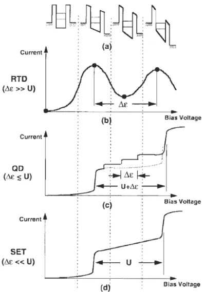
Figure 2-1 Structure of a NMOS transistor ... 30
Figure 2-2 Nanoelectronic devices ... 34
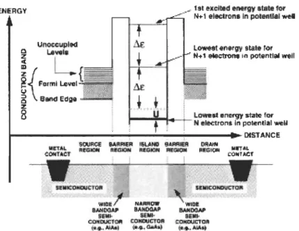
Figure 2-3 Quantum weIl ofa RTD ... 37
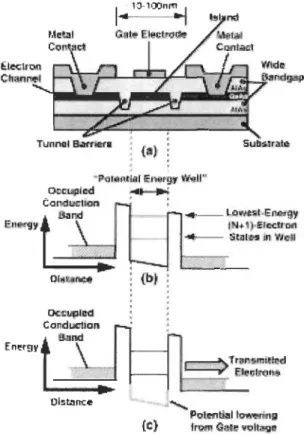
Figure 2-4 Structure ofa RTT ... 38
Figure 2-5 Structure of an RTT ... .40
Figure 2-6 Switching of solid-state nanoelectronic devices ... 42
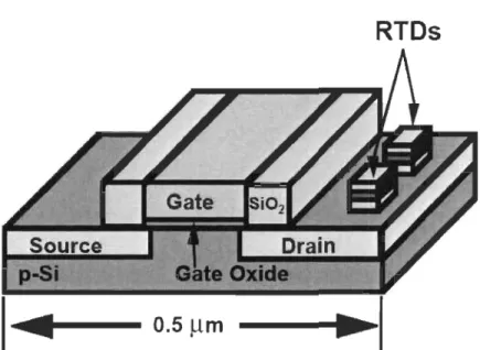
Figure 2-7 A hybrid RTD-FET. ... 44
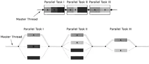
Figure 3-1 OpenMP schematic in comparison to single processing ... 50
Figure 3-2 Placement of the electronic devices ... 55
Figure 3-3 Side-view of the structure ... 57
Figure 3-4 Structure viewed from above ... 58
Figure 4-1 Output characteristics of a 200 nm channel length device ... 74
Figure 4-3 Transfer characteristics of 100 nm and 50 nm devices ... 76
Figure 4-4 Sub threshold slopes ... 76
Figure 4-5 Semi recessed LOCOS process ... 81
Figure 4-6 Preparation for LOCOS process ... 83
Figure 4-7 Mask used in LOCOS process to etch oxide and nitride layers ... 83
Figure 4-8 Finished LOCOS process with bottom gate area to be implanted (red) and oxide (blue) ... 83
Figure 4-9 Amorphous silicon deposited on top of oxide layer, also LPO layer (green) and Nickel (violet) are deposited to start crystallization ... 85
Figure 4-10 Mask used to etch the LPO ... 85
Figure 4-11 Crystallized channel, ready to be implanted with B ions ... 87
Figure 4-12 Mask used to etch the channel silicon ... 87
Figure 4-13 Deposition ofupper gate polysilicon layer.. ... 87
Figure 4-14 Mask used to form the upper gate ... 88
Figure 4-15 Electroless Ni-Au UBM ... 90
Figure 4-16 Reflowed solder bumps on electroless Ni-Au UBM ... 90
Figure 4-17 A "Quad Flat No lead" structure ... 92
Figure 4-18 Pin Grid AITay at the bottom ofa processor ... 93
Figure 4-19 An LGA processor ... 94
Figure 4-20 BGA RAM lCs connected to a PCB ... 95
Figure 4-21 Drain CUITent for different gate lengths ... .1 00 Figure 4-22 Drain current for different gate isolator thicknesses ... 100
Figure 4-23 Drain CUITent for different gate isolator dielectric constants ... 101 Figure 4-24 Drain CUITent for different Gaussian doping profile slopes ... 1 0 1 Figure 4-25 Device parameters ... 1 03
Figure 4-26 Valleys and electron masses ... 107
Figure 5-1 Deviee grid ... 113
Figure 5-2 Algorithm for mode1ing scattering ... 121
Figure 6-1 Speed-up for different numbers of workers ... 145
Figure 6-2 Measured and theoretical speed-up ... 149
Figure 6-3 Measured speed-up is normalized to Gustafson's law's prediction ... 150
C Capacitance
Cox Oxide capacitance
D Si ' D Di effects of source and drain on the local density function for subband i
Dji Local density
E Electric field
Ei Bound state energy of sub band i
Longitudinal en erg y
E pI Maximum energy of subband i
f
frequencyFn Quasi-Fermi energy G Green's function
G+ Hermitian conjugate of G
Gn
, GP Correlation functions describing electron and hole density
G:~ mth diagonal entry of Gn
h Plank constant
1 Current
Drain CUITent
CUITent spectrum at terminal m
Constant
Current in sources of scattering or carrier
J CUITent density
Constant
L Inductance
m Mass
Electron effective mass in z direction •
<m > Average of electron effective mass in the transport direction
n Electron density
n(E,m) Electron density spectrum
Donor and acceptor' s doping concentrations
Grid node numbers in x and z directions
Effective density of states in the conduction band
Electron density constant
P Momentum
P Role density
p Parallelizable percentage of algorithm
p Number of processors
P2D; Constant
q Elementary charge constant
q<T > A verage of electron state lifetime
Q Charge
r Space vector
Ron Channel on resistance
S Speed-up factor
t Time
TSDi(E) Source-to drain transition in terms of electron energy
Tjki Transmission from k to j in subband i
v Speed of electron
Vd Drain voltage
Vdd Operating voltage
Vg
Gate voltage
VGS Gate-source voltage
~ ~h Threshold voltage
,
Vsat Saturation velocity
W Energy
a Non-parallelizable part of algorithm
Beta Caughy-Thomas parameter
Dielectric constant
Body Fermi en erg y
mu low Low field mobility
Iln Mobility of electron
Ils, IlD Contact Fermi energies of source and drain
Il j Fermi potential
Self-energy matrix
L, Lin and LOII1
Self-energy functions
L:: mth Diagonal entry of Lill
\}' (r) Field operator
31/2 Fermi-Dirac integral of order Yi
Introduction
La miniaturisation des MOSFETs a été le carburant de l'industrie semi-conducteur pour
quelque dizaine d'années. L'industrie continuera, probablement, son développement à
l'avenir en créant de nouveaux concepts et technologies. À long terme, pour arriver à une
miniaturisation extrême en comparaison avec l'état de l'art, de nouveaux concepts de
transistors sont prévus pour remplacer les MOSFETs conventionnelles. Même dans la
prochaine décennie, des corrections dans la modélisation et conception des MOSFETs sont
prévues. Au même temps que la miniaturisation arrive aux barrières physiques, de
nouveaux phénomènes voient le jour. L'un de ces phénomènes est le transport balistique.
Le transport balistique et les autres phénomènes reliés à physique quantique, qui
devienne dominant quand les tailles de composant atteignent un certain niveau, ont besoin
d'algorithmes de calcul très lourds pour être modélisés avec précision. L'utilisation des
techniques de calcul à haute performance (HPC) est une solution prometteuse pour le
problème de modélisation et conception de MOSFETs de l'avenir.
Dans ce travail, un outil de modélisation créé par les chercheurs à l'université de
Perdue est employé comme un algorithme qui modélise de nouveaux effets de transport
quantique dans les MOSFETs à double grille. Cet algorithme est parallélisé avec MA TLAB
Canada.
Objectif
Aujourd'hui, la miniaturisation des MOSFETs envisage un obstacle majeur qui est la
consommation de puissance. Dans les technologies courent, la miniaturisation augment la
densité de puissance (figure 1), la génération de chaleur et la température de chip à un
niveau très élevé dans le quel la fonctionnalité et la fiabilité de composant sont menacés
[5].
Densité de chaleur élevée et génération non-uniforme de chaleur, qui est présent dans
les nano-MOSFETs, créent les gradients forts de température [4].
Température élevée pourrais créer des problèmes variés: décharge électrostatique,
électro-migration, surcharge électrique, courent de perte, erreur de synchronisation,
auto-échauffement, point chauds, stress thermique, etc. [4]
Propriétés de transfert de chaleur dans l'échelle macroscopique ne sont pas identiques
avec ces propriétés dans l'échelle nanoscopique. Conduction de chaleur dans l'échelle
nanoscopique est balistique et similaire à radiation thermique [6].
Dans les échelles très petits, «points chauds» de l'échelle nanoscopique, créés dans la
région drain de transistor, augment résistance série de drain et résistance d'injection de
source. Dans les géométries non-conventionnelles qui utilisent nouvelles matériaux (par
exemple dans transistor ultra-mince, finFET ou nanofil) ce phénomène est même plus fort.
En plus, augmentation de ratio de surface à volume dans les nouvelles géométries (figure
2), augment la résistance thermique de frontière des matériaux. Avec les nouvelles
Nouvelles matériaux utilisés dans ces nouveaux composants ont les conductivités thermiques beaucoup plus faible que les matériaux utilisés dans les composants bulks (Table 1) [5]. Figure 1
1000
-NE
u ~100
~1;;
ca
10
1•
4AMD
• Intel • PowerPC -Trend•
•..
•
ri'.
.4•
••
•
1990
1994
1998
2002
2006
2010
Densité de puissance dans le temps ([9])Strained Si, Ge, SiGe
Burled oxide
Bulk Silicon SIlicon substrate
Figure 2 (a) Silicium bulk, (b) Silicium/Germanium tendu sur isolant, (c) composants multi-grille ou FinFET. Conductivité thermique dans technologies plus avancés (b et c) est plus faible. (c) est pris de ITRS
Table 1 Material Si Ge Silicide Si (10 nm) Si02 ([9])
Conductivités thermiques des matériaux utilisés dans la fabrication de semi-conducteurs ([5]) Thermal Conductivity (W/m*K) 148 60 40 13 1.4
En plus, dans les composant où l'une ou plus d'une des dimensions de semi-conducteur de canal est plus petite que « mean free path » d'électron ou phono n, le déplacement des
transporteurs est décrit par les modèles de transport balistique. Transport balistique des particules crée les points chauds et cela change la modèle thermique de composant. Dans ces tailles, où les films semi-conducteurs sont plus minces que «mean free path »,
conductivité thermique de ces films est diminuée à cause de confinement de phonon et diffusion de frontières [5].
Avant arriver à ce niveau de miniaturisation, les points chauds apparaissait qu'à dans le
niveau de circuit et ils étaient reliés à l'architecture de chip. Mais maintenant, avec
miniaturisation extrême, les points chauds nanoscopique sont créés à l'intérieur de transistors [9].
Miniaturisation conventionnelle de CMOS se compose de réduire la longueur de grille et la largeur de diélectrique de grille et augmenter dopage du canal. Dans les MOSFETs plane, dopage élevé du canal diminue les effets de canal court, mais il aussi réduit la mobilité et augment courent de perte. La fonction principale de solutions multi-grille et
« fully-depleted» ultra-mince est de diminuer ces effets indésirables et améliorer la performance.
MOSFETs à double grilles sont les composants avec deux électrodes de grille, placés à
deux côtés opposés du canal. Cette structure donne un meilleur control sur canal. Ces deux électrodes de grille peuvent être deux surfaces d'une grille ou deux électrodes indépendantes, commandés par deux signaux de grille [20].
Présentement, la demande de calcul élevée d'analyse électrothermique nanoscopique
cause des difficultés dans l'optimisation de conception. Pour arriver aux conceptions
Technique rapide d'analyse thermique, basée sur transport classique Fourier, peut servir pour optimiser les conceptions de chips et de refroidissement. Mais cette technique est incapable de décrire les effets nanoscopiques, parce qu'elle manque la description quantique de phonons. D'autres techniques sont développées pour modéliser ces effets: méthodes dynamiques moléculaires, équation de transport de Boltzmann et modèle de diffusion balistique. Mais complexité de calcul reste d'être un obstacle. Il y a beaucoup de différence entre les modèles d'analyse thermique nanoscopique de chip, optimisées pour efficacité et les modèles qui sont optimisées pour précision [14].
Une solution pour le problème de simulation de modèles thermique exigeantes est d'employer les algorithmes parallèles et les implémenter dans les systèmes de calcul à haut performance [15].
Quand la miniaturisation des MOSFETs entre l'échelle nanoscopique, nouvelles effets de nature quantique deviendront important. Dans quelque domaine de conception de MOSFETs (par exemple concentration de dopage ou épaisseur de couche d'oxyde) les couches sont tellement minces que nous pouvons déjà compter les atomes. Dans les autres domaines, ces effets quantiques vont entrer la scène dans le future proche. Pour aller plus loin que régime 10 nm, c'est nécessaire de modéliser ces effets. Mais les simulations précises prennent trop de temps. Facilités de calcul à haut performance créent une opportunité pour ces simulation d'être fais raisonnablement vite et avec la précision désirée.
Dans ce travail, l'objectif est de proposer et implémenter un algorithme de parallélisme pour un outil de simulation des effets b~listiques dans les MOSFETs à l'échelle nanoscopique à doubles grilles. Cela est fait dans le but de diminuer le temps de simulation
pour amver à utiliser les modèles plus précises et faire les recherches paramétriques nécessaire pour conceptions optimisées. Le composant considéré est étudié dans les aspects physiques et mathématiques. Outil de simulation considéré est étudié en détailles et les possibilités de parallélisation dans logiciel MA TLAB sont considérés et comparés. À la fin, l'algorithme de parallélisation est implémenté et le code parallèle est généré et exécuté sur une facilité de calcul à haute performance de Calcul Canada. Les résultats sont présentés, validés (par comparaison avec les résultats de code original) et étudiés concernant l'efficacité de parallélisation.
Méthodologie
NanoMOS, un outil open source développé par les chercheurs à l'Université Purdue, est un simulateur de MOSFETs à double grille à l'échelle nanoscopique. Il considère transport balistique et résout les équations Schrôdinger et Poisson pour trouver les distributions de charge et courent à l'intérieur de composant. Dans ce travail, le code de NanoMOS a été étudié concernant les possibilités de parallélisation et un algorithme de parallélisation a été implémenté sur ce code. Le résultat a été testé en utilisant les facilités HPC de Calcul Canada. Les résultats de simulation et les facteurs d'accélération de temps sont présentés et discutés pour différent nombre de nœuds de calcul. Ce travail, étant une expérience de parallélisation, peut être utilisée dans implémentation d'algorithmes parallèles sur les modèles plus complexes qui facilitent les études paramétriques et optimisations nécessaires pour un design précise de composants nanoélectroniques.
Dans l'exécution parallèle d'un code, la charge de travail est divisée et distribuée parmi différents nœuds de calcul. Idéalement la durée de l'exécution de code va être divisée par le nombre des processeurs engagés. Aussi la mémoire totale disponible sera le résultat de
multiplication de la mémoire d'un processeur avec le nombre des processeurs. Ce qui est
important dans parallélisation, c'est la façon de diviser le job et la méthode de
communiquer parmi les nœuds [15].
Calcul Canada est un collectif de consortia des infrastructures HPC, géographiquement
distribués mais travaillant dans un système unique nationale. Un compte de Calcul Canada,
offert aux professeurs et chercheurs, donne la possibilité de travailler avec les machines de
calcul dans toutes les infrastructures de Calcul Canada et de profiter des supports
techniques, programmes éducatifs etc. [21].
CLUMEQ, l'un des consortia de Calcul Canada, est composé de deux superordinateurs
situé à l'Université McGill, Montréal et Université Laval, Québec [22]:
Colosse: une grappe de 960 nœuds (chacun avec 8 cores processeur et 24 GB de
RAM), totalement 7680 cores et 23 TB mémoire, avec réseau infiniband QDR et capacité
de système de fichier de 1 PB [22].
Krylov: une grappe de 48 nœuds (21 nœuds avec 4 cores et 8 GB de RAM et 27 nœuds
de 8 cores et 16 GB de RAM), totalement 300 cores, avec réseau infiniband SDR [22].
De côté logiciel, NanoHUB est un ressource sur ligne éducationnel et académique dans
la domaine de nanotechnologie. Il inclue cours sur ligne et documents d'apprentissage ainsi
qu'un grand nombre de simulateurs de phénomènes et composants nanoscopiques.
NanoHUB est formé par contributions de plus de 600 chercheurs et éducateurs et le nombre
NanoMOS est un simulateur open source offert par NanoHUB et écrit avec MA TLAB. L'utilisateur a le choix de faire rouler l'outil NanoMOS à distance ou télécharger le code et l'exécuter sur son ordinateur [29], [34].
Modèle conventionnelle de transport de transporteurs est dérivé d'équation de transport de Boltzmann. Cette modèle est basée sur diffusion de transporteurs et décrit bien le cas où canal est longue. Mais dans les composants avec les canaux très courts, modèle quasi-balistique de transport doit être employé, comme il est employé dans NanoMOS. Dans cet outil, formalisme de Fonction non-équilibre de Green (NEGF), qui est une méthode de résoudre des équations différentiels inhomogènes, est employé pour résoudre l'équation de Schrôdinger et calculer les densités de charge et courent. En plus, Équation de Poisson est résolu avec méthode de Newton pour calculer profil de potentiel [20], [29].
NanoMOS a été créé plus tôt avec un regarde algorithmique et mathématique, et pas avec un stress sur codage. C'est parce que le défi, ici, c'est de trouver des solutions pour les problèmes de modélisation physique et résolution des modèles complexe mathématiques et pas faire un codage optimal. MA TLAB a été choisi comme la langue de programmation pour profiter de ses fonctions avancées. NanoMOS a environ 5000 lignes de code distribué dans différents fichiers fonctions de MA TLAB qui sont appelés selon le type de simulation demandé par utilisateur [36].
Pour décrire brièvement la façon de fonctionnement de ce code, il faut dire qu'à part des étapes de donner les entrées, initialisation et calculs primaires, NanoMOS fait ses calculs en un nombre des itérations d'une boucle de calcul. Cette boucle doit satisfaire un paramètre de condition qui représente la convergence de réponses produits par les itérations. À l'intérieur de cette boucle, deux étapes sont pris: au début, fonction
chargenanomos.m est appelé pour calculer la densité de charge en utilisant le modèle de transport choisi. Après, fonction poisson.m est appelé pour calculer le nouveau profil de potentiel en utilisant les densités produites par chargnanomos.m. La différence maximum entre nouveau profil de potentiel et ancien profil de potentiel est comparée avec une critère de convergence, défini par l'utilisateur. Si le critère n'est pas respecté, la boucle est répétée [28].
Après avoir compris le fonctionnement du code, il faut l'étudier pour trouver les stratégies possibles de parallélisation. NanoMOS, en bref, performe un série d'algorithmes de solution des équations sur les nœuds d'une grille de l'espace. Cela est répété pour chaque point de bias. Dans quelque sous-programme de NanoMOS, ces opérations sont faites pour tous les « subbands» et « valleys» d'électrons aussi. Considérant cette structure, quelque stratégie de parallélisation est suggérée. La première c'est de distribuer les calculs en distribuant la grille de l'espace parmi les processeurs. L'autre est de paralléliser sur les points de bias. L'autre solution pouvait être parallélisation de l'algorithme de calcul (effectué sur chaque point de grille et bias) soi-même. Ça vaut dire trouver les possibilités de parallélisation de l'algorithme de solution des équations [28].
Parallélisation sur les points de bias est une solution simple et directe et en même temps inclusif et lourde en termes de routines. C'est simple et directe, parce que c'est l'algorithme le plus claire. Dans NanoMOS, la boucle de calcul principale (solution auto-cohérente) est répétée pour tous les points de bias. C'est inclusif et lourd parce qu'avec cette stratégie, presque toutes les routines de calcul sont engagées dans parallélisation. Chacun parmi eux doit être examiné pour compatibilité avec algorithme parallèle. Ses variables doivent être passés et retournés correctement. Finalement, quand un grand nombre de routines sont
inclus, au moment de faire des modifications ou ajouter des lignes de code, plus d'erreurs doivent être réglées. Les calculs reliés aux points de bias sont indépendants de l'un à l'autre. Elles ont seulement besoin de quelque initialisation, qui est généralement fait à l'extérieur de partie parallèle de code [28].
Pour implémenter l'algorithme de parallélisation sur les nœuds de grille, quelque décision doit être prise. Dans cette approche, des modifications sont réalisées à l'intérieur de toutes les routines qui travaillent avec nœuds de grille. Chaque routine reçoit ses entrées dans la forme des grands matrices qui incluant les données pour tous les nœuds. La routine fait ses manipulations et produit les matrices de sortie. Alors modifications parallèles sont faites indépendamment dans chaque routine. Cela augment « overhead » de cette stratégie. En plus, il faut voir si les routines ont des boucles assez longues pour chaque point de grille. Cela est nécessaire pour que la parallélisation soit efficient. Parce qu'avec les boucles courtes (peu de calcul pour chaque nœud) créer un nouveau nœud de calcul n'est pas profitable. En effet, la plus part des routines n'ont pas des boucles longues désirées. Une solution algorithmique peut être de diviser tous les nœuds de grille en quelque groupe et envoyer les calculs de chaque groupe à un processeur [28].
La possibilité de parallélisation sur « valle ys » et « subband » est plus limitée que les deux solutions discutées. Seulement deux routines répètent leurs calculs pour les « valleys» et« subband» et ils sont, tous les deux, des parties de solution d'équation de transport. Alors dans chaque itération de solution auto-cohérente, juste la moitié d'algorithme est parallélisée. Une solution peut être de paralléliser sur les points de grille quand c'est mieux et paralléliser sur les « subbands» et« valleys» quand c'est préféré. De toute façons complexité et fragilité de cette solution est remarquable [28].
Parallélisation d'algorithme ne semble pas très prometteur non plus. La plus part des calculs sont effectués dans la boucle auto-cohérent, mais les deux routines principales de cette boucle (chargenanomos.m et poisson.m) sont dépendants de résultats de l'un à l'autre. Alors ils ne peuvent pas être exécutés en parallèle. Les autre possibilités de parallélisation d'algorithme ne sont pas assez significatif [28].
Pour conclure, quand il y a plus d'un point de bias, parallélisation sur les points de bias est très efficient; Parce que la plus part de charge de calcul est parallèlisée et aussi parce que peu de communication nécessaire. De l'autre côté plus de routines sont engagées et les paramètres et les appels des routines sont plus nombreux et l'algorithme est plus complexe. Quand il y a juste un point de bias, un mélange des autres solutions doit être utilisé. Dans ce cas, la solution n'est pas aussi efficiente. Parallélisation est moins complexe pour chaque routine, mais il y a un nombre considérable d'opérations parallèles à concevoir et réaliser. Ça vaut dire que les sessions parallèles sont indépendantes pour chaque routine et ça augment « overhead »considérablement [28].
Dans ce projet, NanoMOS est parallélisé sur les points de bias. Une série de points de bias avec tensions de grille identiques et tensions de drain variantes est utilisée pour les simulations. Fonction «parfor » de MATLAB est utilisée pour paralléliser la boucle auto-cohérent de code. Le code parallèle est exécuté sur une grappe et les résultats sont présentés [28], [39].
Codage parallèle dans MATLAB est fait en utilisant «MA TLAB Parallel Computing Toolbox » qui inclut les fonctions parallèles et les fonctions de préparation de réseau de nœuds de calcul. «MA TLAB Distributed Computing Server» est utilisé pour gérer la
grappe et communiquer avec «scheduler» ou «job manager» de grappe. Les nœuds de calcul sont appelés « worker )) et le nœud principal est appelé « client )) [39].
Résultats
Dans ce projet, la diminution de la durée d'exécution de code est le but principal. Facteur d'accélération est le paramètre qui représente augmentation de la vitesse d'exécution. Les limitations de facteur d'accélération sont discutées. En bref, la partie non-parallèlisable de code impose une limite au facteur d'accélération [20], [40].
Comme il est discuté en haut, parallélisation sur points de bias produit le moins «
overhead )) parmi toutes les solutions et abandonne très peu de la charge de calcul à l'extérieur de partie parallélisée de code. En d'autres termes, cette solution a le plus court route critique (route nécessairement sériaI d'exécution) [20], [28].
Code parallèle est exécuté sur 2, 4, 8, 16 et 28 nœuds sur grappe Krylov de CLUMEQ.
Points de bias sont générés avec tensions de drain qui augmentent de 0 V à 1.62 V avec les étapes de 0.1 V. Quand la tension dépasse 1.62 V (pour 28 nœuds) taille d'étapes est diminuée à 0.06 V pour éviter les tensions élevée de drain qui effectue la vitesse d'exécution de code. [22], [39].
Facteur d'accélération est présentée pour différents nombres de nœuds de calcul dans figure 3.
20 18 16 14 12
la
8 6 4 2a
2 workers 4 workers 8 workers 16 workers 28 workers
. speed-up
Figure 3 Facteur d'accélération mesuré par auteur pour différents nombres de processeurs
Considérant les discussions sur algorithme choisi, il est possible de dire que l'augmentation du facteur d'accélération ne sera pas saturée facilement avec une augmentation de nombre des nœuds et la tendance vue dans figure 3 peut être répétée pour les nombres plus grand de nœuds de calcul.
Validation quantitative de ces résultats est faite par comparaison de résultats de code parallèle et code originale. C'est notable que modifications reliées à parallélisation ne changent pas les fonctionnalités de calcul de code. Alors les résultats produits seront identiques. Le vecteur de convergence des donnés est utilisé pour cette validation.
Pour voir l'effet de nombre de « workers » sur efficacité de code parallèle, les facteurs d'accélération produits sont comparés avec la prédiction idéale (sans considérer les communications, initialisations et tolérances) dans figure 4 [28], [41].
30 25 20 15 10 5 0
2 workers 4 workers 8 workers 16 workers 28 workers
Figure 4
... measured speed-up _Gustafson's law's predicted speed-up
Facteur d'accélération mesuré par auteur, et facteur d'accélération théorique
Pour pouvoIr mIeux comparer, les résultats normalisés aux prédictions théoriques idéales sont présentés dans figure 5.
0.9 0.8 0.7 0.6 0.5 0.4 0.3 0.2 0.1 0
2 workers 4 workers 8 workers 16 workers 28 workers
Figure 5
• measured speed-up normalized to Gustafson's law speed-up
Facteur d'accélération mesuré par auteur normalisé pour prédiction de la loi de Gustafson
C'est difficile à reconnaître un motif dans figure 5. La raison est que la durée de l'exécution de code parallèle est de même ordre de grandeur que les tolérances de grappe utilisé. Il a été un des problèmes graves au moment de faire les mesures. Différents techniques ont été utilisés pour diminuer l'effet des tolérances. De toute façon, une pente vers le bas est visible quand l'ensemble des résultats sont considérés. Ça vaut dire que quand le nombre des nœuds de calcul augment, les mesures suivent la prédiction théorique moins étroitement. Cela est à cause de la petite augmentation de la durée de l'exécution pour les points de bias avec tensions de drain plus élevées. Cela cause le code parallèle souffre plus que le code série, alors efficacité diminue. Mais cela ne justifie pas l'utilisation de point de bias concentrer à proximité de zéro (seulement pour avoir des résultats plus idéal), parce que ça ne sera pas la façon que le code parallèle est destiné à être utilisé en
pratique; parce que le changement de point de bias est probablement nécessaire pour optimiser une conception.
Conclusion
Un algorithme de parallélisation est proposé et implémenté sur le code d'un outil de simulation balistique de MOSFETs à l'échelle nanoscopique à doubles grilles. Pour créer une base théorique, différents concepts des composants nanoélectroniques sont étudiés. le composant considéré est étudié dans les aspects physiques et mathématiques et technologiques et les obstacles de sa modélisation sont considérés. Calculs parallèles est proposé comme une méthode de conquérir les obstacles de simulations précises et complètes de ce type de composants. Facilités de calcul à haute performance sous le nom Calcul Canada sont présentés et étudiés comme infrastructures de cette recherche. Un outil de simulation de composant considéré est choisi et étudié en détaille. Les scénarios possible de parallélisation de cet outil dans logiciel MATLAB sont présentés et discutés. Le meilleur algorithme de parallélisation est choisi et implanté et un code parallèle est généré qui est exécuté sur infrastructures de Calcul Canada. Les résultats de calculs parallèles sont présentés et validés. Les résultats sont étudiés concernant l'efficacité de parallélisation. Facteurs d'accélération produits sont satisfaisants et la diminution de la durée de simulation est atteinte comme c'était attendu. Algorithme et code parallèle généré sont accessibles pour travaux additionnelles des chercheurs.
1.1 Nanoscale electro-thermal phenomena
N anotechnology in definition is the science of manipulation of systems with at least one dimension in the range of 1 to 100 nrn. Nanoscale engineering uses different properties of materials in this scale to create new devices [1].
Nanotransistors are one of the most important nanoscale systems and are now subject to great research and study and hopefully will replace today's transistors in near future. Naturally designing and producing nanotransistors with desired characteristics is of great importance. In the following discussion we see that temperature and thermal phenomena, with many other factors, have a huge effect on transistors characteristics. So it is essential to be able to model these effects correctly and efficiently.
Transistors, as one of the main nanosystems, are affected by temperature in different ways: First, transistor delay changes with temperature: higher temperature lowers the threshold voltage and decreases the mobility, causing the delay to change (increase or decrease depending on the strength of each effect).Second, high temperature increases the resistances, causing the interconnect delays to grow. Third, leakage power changes radically with temperature changes. The relation is in fact exponential. Leakage power itself can be very dangerous. This CUITent increases the temperature, so a positive feedback is formed that can lead to the buming of the device. Fourth, reliability problems, for
example negative temperature bias instability (NBTI), oxide breakdown, and electro migration increase with high temperature too [2], [3].
In technologies where the isolation from silicon substrate is created usmg buried
silicon-dioxide layers, because this isolator has a low thermal conduction, self-heating is a more serious problem. Examples are silicon-on-insulator (SOI), strained-silicon-on insulator (SSOI) and tri-gate CMOS transistors [4].
The scaling of transistors has continued for decades now, providing an increasing processing power. Today, this scaling process is facing one major roadblock: power problem. In CUITent technologies, more scaling leads to power densities, heat generation
and chip temperatures so high that the functionality and reliability of operation of the transistors are challenged. Today power density in chips is on the order of 100 W / cm2 [5].
In addition to increased power densities, non-uniform heat generation, which appears in
nanotransistors, creates sharp temperature gradients in these structures [4].
High temperature can cause a wide range of problems: electrostatic discharge (ESD) causing malfunctioning, electro migration and electrical overstress, leakage cUITent, timing failure, self-heating, hot spots, thermal stresses and so on[ 4].
Classical laws of physics do not predict the behavior of systems in nanoscale cOITectly and quantum physics must be employed to predict heat transfer in these scales. For example, Fourier law cannot model the thermal conductivity of super lattices and Boltzmann law is not successful in predicting radiation across small gaps[6].
Sorne of the properties of heat transfer in macro scale are not present in nanoscale,
sorne change. In nanoscale heat conduction is ballistic and similar to thermal radiation. On
the other hand thermal conductivity becomes dependent ofmaterial property [6].
In very small scales a phenomena called nanometer-scale hot spot occurs In drain
region of a transistor, causing an increase in the drain series resistance and source injection
electrical resistances. In non-traditional transistor geometries using novel materials, for
example in ultra-thin body, FinFET, or nanowire transistors, this effect is stronger and heat
conduction is more affected. Aiso increased surface to volume ratio in new geometry
transistors increases the effect of material boundary thermal resistance in the modeling of
transistors that needs attention [5].
New geometries make it more difficult to rem ove the heat generated inside the device
and new materials used in new devices have much smaller thermal conductivities than bulk
silicon (Table 1-1). Aiso when one or more of device dimensions are less smaller than
electron or phonon mean free path, sub-continuum effects, like ballistic electron and
phonon transport, create hot spots in drain and change the thermal modeling of device. In
addition to that, the non-local transport conditions displace these hot spots in a different
way than classical heat diffusion theory prediction and produce a higher temperature rise
than what is predicted by that theory. Just to make it worse, when a transistor has
semiconductor films that are thinner than the phonon mean free path, the thermal
conductivity of these films is reduced because of phonon confinement and boundary
Table 1-1 Thennal conductivities of a few materials used in semiconductor device fabrication, phonon boundary scattering significantly reduces the thennal conductivity of a 10 nm thin silicon film
Pop, E., Goodson, K.E., "Thennal phenomena in nanoscale transistors", The Ninth Intersociety Conference on Thermal and Thermomechanical
Phenomena in Electronic Systems, ITHERM '04. 1-4 June 2004.
Material Thennal Conductivity (W /mK)
Si 148
Ge 60
Silicide 40
Si (10 nm) 13
Si02 1.4
Electron transport is called electrical CUITent and phonon transport is heat flow. When
these two particles' transport is done under Ballistic conditions at nanometer length scales,
a strong non-equilibrium between these energy carriers is caused. It means that the
electron-phonon interaction will no longer be energetically or spatially unifonn. Electrons
transfer their energy to the lattice by interacting with phonons. Optical phonons have no
role in the thennal conductivity. It is longitudinal acoustic phonons that transport heat. This
is the process of generation and transportation of heat in a transistor: applied voltage creates
an electric field with its peak happening in drain. The electric field accelerates and gives
energy to free charge carriers which, in the case of a MOSFET are conduction band or free
electrons. Heated electrons scatter with many particles: each other, lattice vibrations
phonons can transfer energy. In silicon and most of other semiconductors, optical phonon
emission is responsible for most of high field Joule heating. So the phonons take energy from electrons and the lattice is heated by Joule heating. When the lattice's temperature increases, electronic transport properties of the environrnent change. For example, in bulk silicon the electron mobility decreases as T-2
.4 in room temperature [5].
Optical phonons which take energy from electrons are slow moving particles that do not have any role in heat transport. But they decay into acoustic phonons which move fast and transport energy. Electron-phonon scattering time is in the order of tenths of picoseconds. But optical to acoustic phonon decay time is on the order of picoseconds. So that creates a population of optical phonons waiting to decay to acoustic phonons. But now if the generation rate of optical phonons from electrons in the process of Joule heating is greater than the rate of decay into acoustic modes, the population of optical mode phonons increases which, as mentioned above, affects electron transport properties of the environrnent. In the micro-transistors, the volumetric Joule heating rate is the dot product of
the electric field (Ë) and CUITent density (]). But in nanotransistor this is not the case. Electrons are accelerated by electric field mostly in drain, where the field is strongest. Then electrons travel a "mean free path" before scattering with phonons and giving their energy to the lattice. Electrons release their energy to the lattice in several steps over several mean free path travelling. That creates a non-Iocality of phonon emission from the peak of electrical field position in nanotransistors. The electron-phonon mean free path is calculated as the product of electron-phonon scattering time, which is almost 0.05 Pico seconds in the high electrical field, and electron saturation velocity (107 cmls in silicon). So each mean free path is around5 nrn. In micro-scale transistors this distance is negligible compared to
distances around sorne mIcrons, or a little smaller. But in nanoscale transistors with channels with the lengths near 10 nm, it is a big displacement of energy. In other words nanometer-sized hot spots are displaced as much as sorne nanometers from the prediction of continuum theory about their position in drain. This in very small transistors is a significant change and must be modeled to predict the heat transportation correctly [5], [7].
By scaling, the density of devices in a chip increases, but at the same time there is almost no decrease in dynamic power dissipation, so volumetric heat generation density increases in a rate equal to scaling rate. When the dynamic power of due to nanotransistor technologies is considered: C eff Vdd 2 fit seems that reducing operating voltage ( Vdd ) will be ideal for reduction of dynamic power. But to keep the drive CUITent high enough, reducing
Vdd must be accompanied with a reduction in threshold voltage (~). But source-drain
leakage grows exponentially when ~ is decreased. So it is obvious that there is a tradeoff
between performance and power consumption. When threshold voltage is lowered too much to lower the power, the performance suffers. So during the history of scaling, there has been a strong tendency to keep Vdd and ~ high and they have been scaled very lowly
compared with the physical dimensions of devices. So over time transistors have had stronger electric fields and higher power densities. Now the fundamental barriers ahead of this technology have stopped it from continuing to go forward in expense of field magnitude and power density and a major shi ft in process design, performance targets, and
architecture seems inevitable [8].
Dynamic power, being related to impedance, has an inverse relation with temperature. But leakage power increases with junction temperature. It means that if the increase in
power or thermal resistance happens, as it is happening in new technologies, leakage power will grow too. So a positive feedback is formed in which leakage power and temperature start to grow [8].
To sum up so far, as device size reaches 10 nm, circuit density passes one billion devices per centimeter. There is an agreement that the technological roadblock of scaling trend at this point is the power problem. In this view, power densities, heat generation, and chip temperatures are approaching levels so high that reliable operation of devices is no longer guaranteed (Figure 1-1)[9].
Here a more detailed discussion of heat transfer mechanism in lattice is presented. Phonons are Eigen modes of vibration of atoms in the solid state of lattice. This phenomenon is used in describing thermal behavior of materials. These vibrations are divided in two categories of longitudinal and transverse modes. In a different categorization, depending on if the neighboring atoms oscillate in phase or out of phase the phonon associated with the vibration is an acoustic or an optical phonon respectively. The name optical phonon cornes from the fact that an atomic dipole is formed by out of phase vibration, can interact with photons. High energy electrons generate optical phonons which in turn have to decay to acoustic phonons so that heat can be transported from the hot area of lattice. The ballistic travelling of particles makes the bulk parameter of thermal conductivity, which has been used to describe heat conduction in electronic thermal management models, an inaccurate approximation of heat transport for very short times, or very short distances [1].
Although thermal conductivity and heat diffusion equation are still used to explain the majority of thermal transport phenomena at nanoscale, with increasingly high drive fields
they stop responding to the changes, because in these conditions different populations of electrons and phonons are not in equilibrium. In other words, the situation is so far from classical conditions that a single temperature cannot be measured for the lattice. This non-equilibrium of electrons and phonons and also the non-non-equilibrium between optical and acoustic phonons create nanoscale hot spots in short channel transistors. Another factor increasing this hot spot effect is the ballistic electron and phonon transport. Another phenomenon that changes the heat transfer in nanotransistors is thermal boundary resistance, formed at the interface of two solids. Currently there is not any theory to describe the thermal boundary resistance and thermal resistance of nanometers-thick layers.
In sorne tries to describe these effects phonons are supposed to be particles that transport through an interface in a diffusion reflectance model. Sometimes phonons are supposed to be waves and their transport through an interface follows acoustic mismatch model. These theories have not been able to explain sorne of the experimental results. The choice between models depends on roughness of surfaces and scattering at the interface. Thermal conductivity is a bulk parameter; it is the average of effects of many different forms of phonons representing different modes of lattice vibrations. Because it is difficult to calculate each mode's exact share of heat transport, the complete understanding of heat transport in nanodevices is not yet reached [1].
1000
-Ne
u ~ 100 ~~
10 1•
... AMO • Intel • PowerPC -Trend•
1990 1994 1998 2002 2006 2010Pop, E., Sinha, S., Goodson, K.E., "Heat Generation and Transport in Nanometer-Scale Transistors", Proceedings of the IEEE, vol. 94, Issue 8, pp. 1587 - 1601, Aug. 2006 .
. Figure 1-1 Device power density growth over the time. Interesting to note is that the vertical axis is logarithmic and the horizontal one is linear so an exponential trend is obvious. Sorne fact to compare: the power density in a hot plate is in the order of 10 W / cm2 , in a nuclear reactor in the
order of 100 W / cm2 and at the surface of the sun about 7000 W / cm2
. Data compiled by F. Labonte, Stanford
Strained Si, Ge, SiGe
Buried oxide
<a) Silicon substrats ~---~ Bulk Silicon
Pop, E., Sinha, S., Goodson, K.E., "Heat Generation and Transport in Nanometer-Scale Transistors", Proceedings afthe IEEE, vol. 94, Issue 8, pp. 1587
- 1601,Aug. 2006.
Figure 1-2 (a) bulk silicon (b) (strained) silicon/germanium on insulator (c) multiple-gate or FinFET devices. In more advanced geometries (b,c)
thennal conductivity of materials is lower and heat removal is harder. In band c for the gate length of 10-nrn, the thickness of semiconductor is 30% to 50% of the gate length. (c) is from the ITRS [7]
In advanced geometries heat removal is more complicated and harder and new materials, necessary to develop these architectures have lower thennal conductivities than bulk silicon (Table 1-1). It was said that self-heating in nanodevices is due to interaction of electrons and phonons. We saw how electron's mean free path in bulk silicon is about 5-10 nni. Phonons also have their own mean free path that can be calculated to be about 200-300 nrn in bulk silicon at room temperature. When channel lengths in future technologies reaches both these limits, ballistic transport will be the main transport mode of both electron and phonon, in other words, both CUITent and heat. These ballistic transports cause the energy carriers to have a non-equilibrium distribution. It was explained how different phonon modes affect heat flow differently. Worse yet, because ofphonon confinement and boundary scattering in geometries where semiconductor film is thinner than phonon mean free path, the thennal conductivity of the environment will be dramatically less than bulk silicon. So in thin-film and confined-geometry transistors [Figure 1-2 (b) and (c)] heat flow and cooling of transistor is more difficult and temperature is higher than bulk transistors [Figure 1-2(a)] with equal power input [9].
Joule heating, dot product of the macroscopic electric field and CUITent density fails to approximate the microscopie non-Iocality ofphonons in drain. This average model gives no understanding of electron energy exchanges with various phonon modes and it does not provide a spectral understanding ofphonons either [7].
Electrons lose their energy by electron-phonon scattering at a rate equal to the macroscopic relation: P=I.V. In channel lengths bellow 50 nm, phonon distribution
function affects the heat conductivity of the transistor. So the distribution of phonons must
be taken into account in the design. In nanotransistors, for a drain size of around 10 nm
where the field is strong, phonons receive energy from electrons in a distance up to 50 nm
away from drain. Acoustic phonons transport the heat to the contacts and package
boundaries. The propagation of acoustic phonon is faced a resistance when they scatter with
other phonons, impurities, and boundaries. That causes a heat accumulation inside the device and creates higher temperature. More exactly, phonon population is increased inside the device and its effect is represented by a higher effective temperature [8].
Phonon boundary scattering can reduce the effective thermal conductivities ofultra-thin silicon films up to 10 times compared to that of bulk silicon [8].
Within sorne 10nm space around heat source, charge and heat energy transports do not
follow the diffusion model. In this distance, electrons and phonons are in near-ballistic
conditions causing highly non-equilibrium distributions of both electrons and phonons. If
sorne certain quantum effects are small enough to be neglected, the solving Boltzmann
transport equation (BTE) gives almost accurate distribution profiles for different phonon modes, leading to an almost exact profile ofheat distribution [8].
According to simulations, in electric field strengths equal to that of modern transistors,
almost 2/3 of the heat generation is done through generation of optical phonons. But they
are responsible for little to no share of heat transport, because they are much slower than long wavelength acoustic modes. So it is absolutely necessary to find out how these optical phonons decay into acoustic modes [8].
To understand this decay it is necessary to know the optical phonon lifetime for different conditions, inc1uding different power densities [8].
This lifetime has been shown to be about 4 picoseconds for equilibrium conditions in
300 degree of Kelvin. This time decreases as power density of the channel increases [8].
As the channel length is scaled the power density increases. The relation between
power density and channel length for transistors with channel length around 10 nm is
expected to be:
r
l.7
[10].The thermal conductivity of silicon thin films and nanowires in the transistors with
channel lengths beUow 100 nm has been shown by experiment to be two to five times
bigger than that of bulk silicon. This is caused by phonon surface and interface scattering
[1] .
In macro scale, many different carriers are involved in heat transfer: phonons, electrons,
photons are molecules. They aU behave like partic1es in these scales. In nanoscale on the
other hand, carriers show wave behaviors a lot more often, so that the wave effects are
often more important than partic1es behaviors, though that is not always the case[ Il].
Mean free path of a partic1e is the distance it travels between two collisions with other
partic1es. These collisions can happen with two different types of partic1es. Nanoscale heat
transfer phenomena can be seen in five categories depending on the relative sizes of mean
free path and channel length [11].
When the structure is much bigger than the mean free path of the carriers, the diffusion
regime can safely be used. This model then can be solved using conventional methods.
Now depending on the relative size of the structure to the mean free path of energy carriers,
i.e. electrons and phonons, two distinct regions can be identified. Inside each region a
particle properties. There are also two transition zones where the size is comparable with the mean free path of a carrier and using one regime means accepting sorne approximation. In these zones scattering process that takes place in the environment determines if the diffusion regime should be used or ballistic regime. If scattering destroys the phase of the wave, the wave effects die out and diffusion can be used with sorne approximation. Inelastic scattering occurs when inelastic collisions, for example collisions between electrons and phonons or between phonons and phonons, destroy the phase of the wave. The when the structure is smaller than mean free path and the ballistic regime is used, it means that the scattering is neglected [11].
The ballistic behavior happens in highly scaled transistors when power density is above 1000 W / cm3 and channel length is well below 100 nm, in other word much less than relaxation length. In this situation the behavior of "hot electrons" and "hot phonons" needs to be analyzed [12].
The non-equilibrium situation of energy transport in nanotransistors changes their behavior to a great extent. This phenomenon reduces the trans-conductance of the transistors, in other word, the drive CUITent. Aiso it can increase sub threshold leakage power. These changes occur due to the fact that when electrons scatter and transfer their energy to optical phonons, because these phonon modes have low group velocities (~ 1000 mis), they cannot transport the heat from the hot region. In 10 picoseconds they decay into fast moving acoustic phonons. But the delay means that there is an increase in energy density near hot spots, which affects electron transport [12].
So, nanoscale sizes create nanoscale hot spots in the transistor's drain, and that increases the drain series and source injection electrical resistances through creation of high
densities of carriers. This process is helped by use of new materials and modem geometries
like ultrathin body, FinFET, or nanowire devices. Thermal analysis in these cases differs
from classical diffusion theory and sub-continuum phenomena like ballistic electron transport play an important role in heat generation and heat transport [9].
Aiso in new geometries there is a greater surface to volume ratio which means
boundary thermal resistance has a larger effect on heat transport in modem transistors [9].
Now that it is observed that heat conduction in nanostructures is much more limited
than anticipated by the Fourier theory and that size effects produce higher temperatures,
more effective thermal management measures have to be taken. As a positive side, these
size effects might also offer the possibility of developing highly efficient thermoelectric
(TE) materials and more efficient thermal management through direct cooling [13].
Size effects can cause limited heat conduction capability in super lattices of nanotransistors, which produce sorne thermal problems. But these effects also enhance the properties of thermoelectric (TE) devices, used in thermal management of semiconductor lasers. Maybe they have the same effect on thermal management of microelectronic devices too. In fact a factor called TE figure of merit (FOM) that indicates the efficiency of TE
coolers, has shown high numbers in sorne III-V super lattices and TE super lattices
meaning low thermal conductivities [13].
Heat transfer at macro scale follows sorne principle rules. One of them is the Fourier
law that is basically a diffusion equation. Another useful factor to describe thermal
behavior in macro sc ale is thermal conductivity which is a material property and independent of size and shape [6].
High power density and temperature in electronic circuits reduces transistor carrier
mobility and threshold voltage and increases interconnect resistance, it produces reliability
problems like electro migration, dielectric breakdown, and negative body biasing. It also
increases power consumption by increasing sub-threshold current. At the end cooling costs
increase because of all the negative impacts of scaling on thermal management [14].
To solve a heat generation problem within the classical limits, Joule heat generation
rates are calculated as dot product of electric field and CUITent density. Temperature profile
can be found by solving heat diffusion equation derived from Fourier law. This method is
applicable when the assumption that electrons and phonons, as current and heat carriers, are
in local equilibrium is valid and also when the discussed sizes are bigger than sorne
mean-free-paths of carriers [12].
Self-heating in semiconductor device is a production of scattering of electrons with
phonons. To find a fairly exact model of this process all of the scattering events have to be
considered in the simulation. Solution of the Boltzmann Transport Equation (BTE) for both
electrons and phonons can provide this goal. BTE is a semi-classical transport regime in
which charge and energy carriers are particles between scattering events [12].
1.2 Problem
In thermal aspect of micro and nanoelectronics two problems can be identified. One is
the process of heat generation, heat transport and heat conduction in each device and the
other one is the heat management at a system level [6].
Today, thermal management has to be applied at all levels of system. It starts from
transistor and continues to the circuit and microarchitecture and finally to the packaging.
However in modern thin-body devices with higher field levels thermal management within
the transistors has become more important than before [10].
Before, hotspots used to appear only at the circuit level, due to the architecture of
devices on the chip. Now, nanoscale hot spots are starting to appear inside the transistors
[9].
Micro- and nanoscale electronic devices are capable of producing heat fluxes in small
hot spots in the order of sorne thousands of watts per centimeter square. In the chip level
sorne areas as big as a couple of hundred micrometers in diameter with a temperature
10 - 400 C hotter than the surroundings can be formed because of difference in the work
load of transistors. Naturally cooling systems are designed to fight the highest temperature
on the chip and because the cooling systems usually cool all the area of the chip, this means
that sorne of the cooling resources go to waste because of hot spots. If the hot spots are
removed by correcting the design, cooling costs decrease, or there will be more cooling
resources and more densities of devices become practical. The same goes for the nanoscale
hot spots formed in the nanotransistors. In bulk silicon devices, the thick silicon substrate
(sorne several hundred micrometers thick), with its high thermal conductivity, absorbs the
heat from hot spots and distributes it to a size comparable to its own thickness. This is still
much smaller than the whole circuit size, but one can observe that in this way bulk silicon
substrate softens the extremely non-uniform power dissipation patterns. Now when the
silicon wafer becomes thinner and wh en stacked chips or three dimensional chips are