HAL Id: hal-00761020
https://hal.archives-ouvertes.fr/hal-00761020
Submitted on 4 Dec 2012
HAL is a multi-disciplinary open access archive for the deposit and dissemination of sci-entific research documents, whether they are pub-lished or not. The documents may come from teaching and research institutions in France or abroad, or from public or private research centers.
L’archive ouverte pluridisciplinaire HAL, est destinée au dépôt et à la diffusion de documents scientifiques de niveau recherche, publiés ou non, émanant des établissements d’enseignement et de recherche français ou étrangers, des laboratoires publics ou privés.
Superconducting group-IV semiconductors
Xavier Blase, Etienne Bustarret, Claude Chapelier, Thierry Klein, C. Marcenat
To cite this version:
Xavier Blase, Etienne Bustarret, Claude Chapelier, Thierry Klein, C. Marcenat. Superconduct-ing group-IV semiconductors. Nature Materials, Nature PublishSuperconduct-ing Group, 2009, 8, pp.375-382. �10.1038/NMAT2425�. �hal-00761020�
Superconducting Group IV Semiconductors
Xavier Blase1,2, Etienne Bustarret1,3, Claude Chapelier4, Thierry Klein1,5 and
Christophe Marcenat4
1
Institut Néel, CNRS, B.P.166, 38042 Grenoble Cedex 9, France
2
Laboratoire de Physique de la Matière Condensée et Nanostructures, Université Lyon I, UMR CNRS 5586, F-69622 Villeurbanne Cedex, France.
3
Departamento de Ciencia de los Materiales, Universidad de Cadiz, 11510 Puerto Real, Spain
4
CEA, Institut Nanosciences et Cryogénie, SPSMS-LATEQS, 17 rue des Martyrs, 38054 Grenoble Cedex 9, France
5
Institut Universitaire de France and Université Joseph Fourier, B.P.53, 38041 Grenoble Cedex 9, France
We present recent achievements and predictions in the field of doping-induced superconductivity in column IV-based covalent semiconductors, with a focus on B-doped diamond and silicon. Despite the amount of experimental and theoretical work produced over the last four years, many open questions and puzzling results remain to be clarified. The nature of the coupling (electronic correlation and/or phonon-mediated), the relationship between the doping concentration and the critical temperature (TC), which determines the prospects for higher transition
temperatures, as well as the influence of disorder and dopant homogeneity, are debated issues that will determine the future of the field. We suggest that innovative superconducting devices, combining specific properties of diamond or silicon, and the maturity of semiconductor-based technologies, will soon be developed.
1) Introduction
It was probably the discovery of a superconducting transition around 40 K in the rather simple MgB2 compound[1] that revived the interest for a specific class of
superconducting materials, belonging to the so-called covalent metals[2]. These superconducting covalent systems (see box 1), including B-doped diamond[3], silicon[4] , and silicon carbide[5,6] , Ba-doped silicon clathrates[7,8], alkali-doped fullerenes[9,10] and the CaC6 or YbC6 intercalated graphites[11,12], share the
specificity of involving at least one relatively light element and of preserving strongly directional covalent bonds in their metallic state. The implications of this
covalent character are important in superconductors in which Cooper pairs are coupled through phonons. The use of perturbation theory to study the renormalisation of the electron-electron repulsion by the electron-phonon interaction leads to the so-called Eliashberg equations[13] and to the celebrated McMillan formula[13] relating, in an approximate way, the superconducting transition temperature TC to an average phonon frequency ωln, the electron-phonon
coupling parameter λep and the screened and retarded Coulomb repulsion
parameter µ*: 11 TC = 2ωln 1.2kB exp −1.04(1+λep) λep−µ * (1+0.62λep) 1 2 3 4 5 6
Clearly, low atomic masses lead to high frequency phonon modes, which may enhance the ωln prefactor and thus TC. This is the basis of the so-called isotope
effect. Furthermore, strong covalent bonding will lead both to large phonon frequencies and a large electron-phonon coupling potential Vep=λep/N(EF), with
N(EF) the density of states at the Fermi level, also contributing to enhance TC. Even
within a phonon-mediated coupling scenario, these criteria do not necessarily warrant a large TC since increasing λep may also lead to a lattice instability, and a
large electron-phonon potential Vep may be impaired by a low density N(EF).
However, these simple considerations, as well as more elaborate surveys and predictions of a larger TC
[14-16]
, have provided much incentive to study this class of materials.
The most familiar covalent systems are certainly diamond and silicon. The former can be considered as the prototype insulating material with unsurpassed incompressibility and hardness, and the latter is the textbook semiconductor, which has laid the grounds for today’s electronic industry. When the doping concentration in semiconductors (or insulators) goes beyond a critical value, a metal-insulator transition (MIT) takes place (see box 2), turning the host material into a degenerate semiconductor with the Fermi level entering the valence (conduction) bands in case of p-type (n-type) doping, and eventually into a superconductor. Turning diamond into a metal clearly makes this system an ideal candidate for superconductivity as it offers all the qualities listed above, with very directional bonds and optical phonons in the 150 meV range (compared to a few tens of meV in classical metals). This is where recent breakthroughs in the synthesis of highly doped diamond[3], silicon[4,17] and silicon-carbide[5,6] samples come in.
2) Superconducting semiconductors : from early predictions to recent discoveries
The idea that semiconductors doped beyond the MIT could become superconducting was already discussed in the mid-sixties[18,19]. Superconductivity was observed subsequently in reduced SrTiO3 perovskite single crystals [20,21] and
in Ge1-xTe alloys[22]. However, the interest in superconducting doped-semiconductors did not last, probably because of the low critical temperatures (at most 0.5K[21]).
We will not discuss here in detail the case of the fullerenes for which excellent reviews have been written (see for instance[23,24]). The evolution of the electron-phonon coupling strength with cage curvature, the large value of the ωph/W
(coupling phonon frequencies to electronic bandwidth) ratio, the proximity of a MIT driven by electronic correlations (see Box 2), and the local nature of the coupling phonons (Jahn-Teller modes) are however aspects that will be relevant to the cases of doped diamond and silicon as discussed below.
In 1995, it has been shown[7] that barium-intercalatedBa8Si-46 clathrates undergo a
superconducting transition around 8 K (see also[2,8]). Silicon clathrates are 3D semiconductors made of face-sharing Sin clusters (n = 20,24,28) as building
blocks[25] (see box 1). Such systems are very close to standard silicon, each atom being fourfold coordinated with a local sp3 tetrahedral environment, but with a cage-like structure that allows large doping by intercalation at the centre of the cages. Ab initio calculations proved that the phonons involved in the transition were mainly the silicon network vibrational modes, while barium would serve as an n-type dopant[26]. This was the first evidence that highly-doped column-IV sp3 covalent insulators, or semiconductors, could be turned into superconductors with a TC exceeding a few Kelvin.
On the other hand, research efforts were also quite intense in the apparently distant field of superhard materials belonging to the B:C:N chemical composition triangle. While diamond still stands out as the hardest crystal known, the significant hardness of other materials such as B4C, BN or BC2N has stimulated creative
synthesis strategies : in 2004, two groups[27,28] performed High Pressure High Temperature (HPHT) treatments to obtain carbon borides, but also got highly doped (2-3 at.%) polycrystalline diamond. Then, bridging the gap separating the super-hardness and superconductivity communities, doped diamond was found to be superconducting around 4K[3], paving the way for systematic studies of super-hard superconducting materials[29]. Since then, superconducting polycrystalline,
single crystal or even nanocrystalline boron-doped diamond samples have been synthesized by a large number of groups using the original HPHT [30] techniques or alternative chemical vapor deposition growth techniques[31-35], and transition temperatures up to 10 K have been reported[36].
In 2006, using a gas immersion laser doping (GILD) technique (see box 3), which allows to dope silicon well beyond the thermodynamic solubility limit, a superconducting transition in highly boron-doped silicon was reported with a TC
around 0.35 K for a boron concentration of the order of 8 at.%[4,37]. Finally, a superconducting transition was also observed recently in boron-doped SiC[5,6] with a TC of 1.4 K. In all three cases (diamond, Si and SiC), boron was the source of
hole-doping.
3) Phonon-mediated or correlation-driven mechanisms ?
The question “where are the electrons?” takes a special twist in doped semiconductors[38] since across the MIT, the Fermi level is expected to shift from an impurity band to a degenerate situation where it is located in the valence bands (for
p-type doping, see box 2). The coincidence of the superconducting transition with
the MIT in doped diamond has triggered much experimental and theoretical work to understand the character of the electrons at the Fermi level involved in the superconducting transition, and the origin of the attractive interaction leading to Cooper pairs. Indeed, when the Fermi level is located in a narrow electronic band, the so-called resonant valence band (RVB) model can explain a superconducting transition with a specific pairing mechanism, alternative to the standard phonon mediation. Besides the case of doped diamond[39], such a correlation-driven mechanism has for instance been proposed in the case of doped fullerenes[40,41].
Ab initio calculations within density functional theory performed on highly-doped
diamond[42-47], silicon [4,48] and silicon carbide[49] consistently led to the picture that in the percent doping range, the Fermi levels lies a few tenths of an eV below the top of the valence bands. These results where obtained either within the virtual crystal approximation (VCA)[42-44] or supercell (SC)[45-47] calculations for various cell geometries and doping concentrations. Furthermore, the effect of disorder on the electronic properties was studied with the coherent potential approximation (CPA)[50] leading again to the picture of a degenerate system with the Fermi level entering the valence bands broadened by disorder. This degenerate picture with no signature of an impurity band has been rapidly confirmed by experimental angle-resolved photoemission experiments performed on diamond films[51]. Additional evidence for deep localized states in the gap came from element-sensitive soft
X-ray emission and absorption spectroscopy, together with the conclusion that in the bulk of a superconductive sample, the Fermi level of the normal state was lying below the top of the valence band, in a region where boron-related delocalized states are also present[52]. However, these theoretical and experimental results were obtained in the very large doping limit, away from the MIT transition, and the question of what happens close to this transition remains open.
In the absence of a narrow impurity band, the best guess for explaining the superconducting transition is the phonon-mediated mechanism. Ab initio simulations explored this mechanism by calculating the electron-phonon coupling parameter λep again within a variety of VCA and SC approaches. For typical
doping concentrations of a few percent, λep was found to range between 0.3 and
0.5, values which are consistent with the experimental TC values assuming that the
retarded Coulomb pseudo-potential µ* ~ 0.1, a typical value for metals. However, the absence of substitutional disorder in ab initio SC and VCA calculations, as well as the possibility to adjust the parameter µ*, may impair the conclusiveness of such calculations. It is worth noting in this respect that the very large value of the phonon energy (~ 120 meV) is comparable to the Fermi energy, leading potentially to a much weaker screening and a larger µ* value than in usual metals. Furthermore, Migdal’s theorem [53], which exploits the decoupling of electronic and phonon energies to remain at lowest order in treating the electron phonon-interaction as a perturbation, is in principle violated, so that strong non-adiabatic effects and deviations from the standard Bardeen-Cooper-Schrieffer (BCS) [54] theory may be expected. However, accurate dynamical mean-field theory calculations in the case of fullerenes, presenting a similar electron to phonon energy ratio, led to the conclusion that for λep lower than ~ 0.5, the standard
Migdal-Eliashberg approach and more accurate many-body treatments of electron-electron and electron-electron-phonon interactions provide equivalent results[41]. From an experimental point of view, scanning tunnelling spectroscopy measurements[55] performed on boron-doped diamond led to a 2∆(Τ)/kBTC ratio with a thermal
dependence perfectly matching the BCS weak-coupling limit[13] (∆(Τ) being the temperature-dependent quasiparticle band gap). Such a weak coupling limit is indeed expected for electron-phonon coupling since TC is much smaller than the
characteristic phonon energy. However, this result does not exclude any other weak coupling mechanism. Recent attempts at isotopic 12C by 13C substitution in polycrystalline superconducting samples grown by HPHT[30, 56] provide preliminary evidences for a strong isotope effect on TC : the reported exponent is larger than
If one assumes that the electron-phonon coupling scenario is valid, one still has to answer the question: « where are the phonons? », or, rather : “which phonons contribute to the coupling with the electrons?”. The role of low-momentum optical modes has been emphasized by VCA simulations [42-44]. An analysis of the phonon sidebands appearing as Fermi edge replica in photoemission spectra [58] and of the softening of zone-centre optical modes in inelastic X-ray scattering has been interpreted in this sense [59], although the observed softening was significantly smaller that that predicted by VCA. On the other hand, SC calculations for diamond [45-47] lead to a spectral distribution of the electron-phonon coupling parameter with a major contribution from the dopant-related stretching mode. A Kramers-Kronig analysis of reflectivity measurements [60] supports a possible contribution of boron-related vibrational modes. However, the experimental identification is difficult as the B-C stretching modes frequencies lie in the continuum of bulk diamond modes. Localized dopant-related vibrations could be easily identified in boron-doped silicon, since the B-Si stretching frequency is 60 cm-1 above the bulk silicon zone-centre optical modes[4]. Clearly, the influence on TC of isotopic substitutions (
11
B by 10B) will bring much insight intoon the relevance of dopant-related modes [56, 61]. However, the amount of substitutional boron in samples of distinct isotopic contents is quite difficult to control with the experimental precision needed to provide unquestionable evidence for an isotope effect.
4) Greatness and misery of superconducting doped diamond and related compounds
Why should we bother about superconducting semiconductors ? Clearly, doping an insulator to turn it into a metal does not sound like the most straightforward way to obtain a good superconductor. As briefly mentioned in the introduction, the first answer lies in the strength of the electron-phonon coupling. As a matter of fact, in covalent metals, the electron-phonon potential Vep turns out to be extremely large.
This is precisely due to the covalent character of the bonding.
Along that line, p-type doped diamond is exceptional: the deformation potential associated with the zone-centre optical modes of diamond (sp3 bonds) was estimated[42,43] to be ~ 50% larger than that associated with the E2g mode in
MgB2[42]. It may then sound surprising that the largest TC in doped diamond (~10K)
is significantly smaller than in MgB2 (39 K). The explanation lies in different
values of N(EF). While the layered MgB2 compound benefits from a strong 2D
density of states, the density of states in 3D materials slowly rises with the square root of the Fermi energy. Larger chemical doping, alternative charge injection
techniques, or patterning into low dimensionality geometries, are potential solutions that remain to be explored.
A couple of interesting attempts to estimate quantitative bounds for the maximum phonon-mediated superconductivity in covalent metals have been proposed recently[14-16]. The analysis of the density of states and so-called effective McMillan-Hopfield parameter[15] led to the conclusion that, in randomly substituted cubic BxC compounds, TC could increase with doping up to 60 K for x ~0.3 within
a rigid band model and assuming that µ*~0.12. Similarly, it was also predicted[16] that TC could be equivalent to that of MgB2 in the cubic BC5 structure. Previous ab
initio calculations suggested that carbon-doped boron icosahedra could be very
good candidates for high TCs [62]
.
Experimentally, however, the relation between boron content and TC is quite
unclear. The above mentioned BC5 structure has recently been synthesized using an
HPHT technique [63], but the nanocrystalline nature of this phase precluded any characterization of the superconducting properties so far. Similarly, a highly-doped diamond-like BC1.6 structure was synthesized
[64]
, but no trace of superconductivity was reported. Furthermore, it has been observed that increasing the doping concentration of diamond above a few percents does not necessarily lead to higher TCs and that similar boron contents could lead to a wide range of TC values[31-34].
This was suggested to result from the clustering of boron in inactive dimers[65,66] or from an increase in interstitial boron content[65]. The aggregation of boron at grain boundaries in polycrystalline diamond has also been recently reported in HPHT synthesized samples[67].
An alternative route to high critical temperatures relies on the cage structures. The efficiency of sp3 bonding in driving a large electron-phonon coupling, has been first highlighted in superconducting fullerenes[68]. It has been shown through a combination of experimental and theoretical studies that Vep increases dramatically
from C60 to C28[69] and finally C20[70] cages. Indeed, by reducing the radius of the
cage, one increases the sp3 character of the bounds. Similar effects can be observed in carbon nanotubes where the coupling strength increases with decreasing diameter[71], consistently with the evolution of the superconducting transition from 0.3 K in large diameter tubes[72] to 14 K in 4 Å diameter tubes synthesized in AlPO4
zeolite channels[73]. Several other carbon-based structures with a large percentage of sp3 bonds have been synthesized[74] but have only been considered so far for their application as ultra-hard materials [75,76]. These arguments for the increase of the electron-phonon coupling strength from sp2 to sp3 bonding should however be treated with care as confinement effects in small fullerene cages play an important
role[77]. Furthermore, recent ab initio calculations of the deformation potential in graphene indicates values which are definitely not negligible when compared to diamond [77,78].
As mentioned in section 2, the potential properties of those cage structures have also been illustrated in the case of the silicon clathrates, which are all sp3 silicon-based cage-like structures. Contrary to fullerenes, the atoms in clathrates have four neighbours and all sp3 bonds are fully saturated without any dangling bond character. Due to the presence of pentagons that frustrates the formation of bonding
p-states at the top of the valence bands, electronic bands flatten as compared to
their diamond analogue, leading to a large density of states[80]. Furthermore, the cage structure allows large (endohedral) doping and provides much more flexibility in the doping chemistry. In particular, in barium-doped clathrates, the hybridization of the Ba 5d orbitals with the Si 3p orbitals further contributes to significantly enhance N(EF), leading to a rather large λep value close to 1[8,26]. As a result, the
transition temperature in barium doped Si clathrates is ~8 K for an all silicon based
sp3 materials that can be compared to the 0.35 K value found in boron-doped cubic silicon. Unfortunately, and despite several attempts, carbon clathrates have not yet been synthesized and their potential interest as superconducting materials remains limited to theoretical predictions of TC as large as 77 K
[81]
. This speculated TC can
also be found in the figure of Box 1. Finally, CnBm clusters have been
produced[82,83], but to our knowledge the synthesis of BC clathrates has never been reported.
We conclude this section by mentioning the case of layered graphitic structures such as CaC6 or YbC6
[11]
and related structures (see also box 1). In contrast to MgB2, the Fermi level in CaC6 or YbC6 does not lie in the σ-band (in-plane sp2 covalent bonds) but remains located in the π-band (out-of-plane pz-bonds). Nevertheless, the hybridization with intercalant states, the so called ζ-band, still ensures a rather large TC value of up to 11.5 K, thanks to the existence of soft
phonon modes. It is hence very tempting to look for systems combining the advantages of both systems: strong electron-phonon coupling of the covalent σ -band and interlayer states coupled with soft intercalant modes. A promising candidate was the Li2B2 system for which the Fermi level indeed lies in both σ and ζ bands[84,85]. Unfortunately, the “accidental” loss of the π electrons leads to a hardening of the phonon modes and reduces λep to ~ 0.6 as compared to MgB2 for
which λep ~ 1.0. Many theoretical works have recently been devoted to the search
forof new graphitic-like structures which would optimize the coupling with the various bands. Among those, systems such as BC3[86] or LixBC[87] (x<1), with TC
valuesup to 150K, were predicted. Unfortunately these predictions have not been verified experimentally so far. The use of ab initio simulations to explore the thermodynamic stability of potential superconducting phases may prove quite useful in the future as illustrated recently in the case of the hypothetical antifluorite Be2BxC1-x phases[88].
5) Forthcoming potential applications
In Superconducting-Normal (SN) junctions, phase coherent transport can be induced in the normal (N) conductor by the so-called proximity effect. The mismatch between the electron densities at the Fermi level and the existence of a Schottky barrier severely limits the leakage of Cooper pairs through the junction and the functionality of superconducting devices when the N element is a semiconductor[89]. In this respect, indium arsenide (InAs) is an exceptional semiconductor[90] since it can form Schottky-barrier-free contacts with metals. However, in this case, the Josephson current remains low due to disorder. The superconductivity of ultra-doped Si could then provide a new paradigm in the field of such junctions, since the two regions can be made out of the same material by simply changing the doping level, thus avoiding problems with interface Schottky barriers. The GILD technique allows fabrication of ultra-shallow highly doped regions with abrupt interfaces (< 2 nm/decade in boron concentration). This will allow the fabrication of mesoscopic SNS junctions with sub-micrometer separation between superconducting electrodes. Control of the Josephson current and the current-voltage characteristics could be achieved through additional capacitive gates which affect the electronic density in the normal region, leading to the fabrication of a Josephson field-effect transistor (JOFET) [91].
The discovery of superconductivity in Si, SiC, and diamond also gives the possibility to design new superconducting NEMS (Nano-Electro-Mechanical Systems, for a review see[92] ). In a monolithic device, superconducting electronics can now be integrated to a NEMS oscillator for quantum-limited detection of force, mass, charge, or displacement. The zero electrical dissipation and the absence of an additional metallic layer deposited onto the resonator increase the quality factor and the sensitivity of actual systems, and new fundamental effects could be observed due to the coherent nature of superconductivity (see for instance [93]). In particular, the outstanding physical, electronic, and thermal properties of diamond make this material unique for the development of NEMS devices. The unmatched Young modulus will allow the achievement of higher frequencies ν (GHz)[94] than in state-of-the-art mechanical resonators and hence to reach the quantum limit (kBT < hν) at
and a large second critical magnetic field, of a few Tesla, both larger than in conventional superconductors, also provide the possibility to operate at higher magnetic fields and to reach a stronger electromechanical coupling regime.
6) Conclusions and open questions
Since doped diamond stands out as the archetype of superconducting covalent metals, we may identify several short-term research directions dealing with this material, partlyapplicable to the other systems covered by this review:
a) Further exploration of the dopant and host atoms isotope effects would certainly bring much information on the relevance of the phonon-mediated mechanisms and on the nature of the important vibrational modes (bulk optical states or localized boron-related modes). At this point, any experimental signature from the coupling phonons would be welcome.
b) More detailed empty state spectroscopy (e.g. by inverse photoemission or high resolution X-ray absorption) complementing the published ARPES measurements[51], would help to confirm the presence of an empty impurity band and/or deep inactive boron-related levels in order to understand the coupling mechanisms and the relation between impurity and free carrier concentrations.
c) Calculations of TC and 2∆(Τ) within the recently developed density functional theory for superconductors [95,96] will suppress the need to adjust the µ* value. This approach was tested on several simple materials showing excellent agreement with experimental transition temperatures and quasiparticle band gaps.
d) The nature of the superconducting transition (type I or type II) also has to be clarified. Tunnelling spectroscopy measurements unambiguously proved the existence of vortices in C:B epitaxial films[55] (i.e. type II superconductivity) and the high values of the critical fields observed in Si:B (~ 0.4T for TC~0.35K[4]) strongly suggest that this system is a type II superconductor.
On the other hand, superconductivity was found to be of type I in 3C-SiC[5,6] (Hc~0.01T for TC~1.4K). Note that, in the dirty limit when the mean free
path l is much smaller than the coherence length ξ, κ (=λL/ξ) is renormalized
to λL/l, λL being the London penetration depth and a clean type I
superconductor (κ<0.7) might be turned into a dirty type II superconductor. e) Another fundamental aspect in superconducting semiconductors is the new
playground it offers for studying the interplay of disorder-induced localization, Coulomb interaction and superconductivity in the vicinity of a disorder-driven Mott-Anderson transition [97,98] (see Box 2). For instance, TC
remains anomalously high down to the transition in boron doped diamond[99] whereas, in the BCS picture, it is expected to become exponentially small as
λep tends towards zero at the MIT. On the contrary, it was recently proposed [100]
that close to a mobility edge (disorder induced MIT) TC may only drop
as λep1/γ (γ being a scaling exponent) suggesting that disorder may play a
significant role in boron doped diamond. The simultaneity of these two transitions here offers new opportunities to study this issue in detail.
More generally, it will be desirable to increase TC in each system. Aluminum doping of silicon has for instance been calculated to be more effective than boron for superconductivity [48], but its substitutional incorporation at levels in the at. % range remains a challenge. An insulator-to-metal transition has been recently induced by aluminium doping in 4H-SiC epilayers [101] but without any evidence for superconductivity. Although ab initio calculations can provide useful hints about alternative materials and favourable stoichiometries or dopants, progress in this direction is now limited by material preparation issues. Various hypothetical systems such as carbon clathrates, highly doped (20 to 30%) cubic diamond, LixBC have been predicted to yield large TC values but the
synthesis of such systems remains elusive.
A lower disorder may also be beneficial [97]. Recent improvements of the growing process (GILD technique) increased the critical temperature of Si:B by a factor 2[102]. As mentioned, Si:B might also play a fundamental role in the development of SNS based devices. The use of (InAs-based) JOFETs hasve so far been hampered by low critical Josephson current and interface disorder. A silicon-based technology could then open the way to the possibility of fabricating flexible proximity circuits, in which several parameters of the normal and the superconducting electrodes could be tuned to achieve new effects in quantum electronics.
Box 1 : Covalent structures
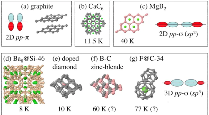
It is well-known that under ambient conditions, carbon crystallizes mainly in the diamond (sp3) and layered (sp2, graphite) structures. In its graphite form the Fermi level (EF) lies within the π bands formed by 2pz out-of-plane orbitals (Fig. 1a).
The lateral superposition of these orbitals is expected to lead to a small electron-phonon coupling constant. However, what makes those systems particularly interesting is the possibility of modulating their electronic structure by doping. Vibrations perpendicular to the plane, as well as intercalant modes, can for instance couple quite efficiently with the nearly-free-electron-like band that crosses EF in the intercalated CaC6 compound (so-called ζ band, Fig. 1b) leading
to TC values of up to 11K.
However, the best coupling constant is expected to be obtained for the lower energy σ band which arises from in-plane 2pxy orbitals (sp2 coupling, see picture 1c). Indeed, the direct axial superposition of atomic orbitals makes them very sensitive to atomic vibrations leading to high electron-phonon coupling constants. Bringing the Fermi level into the σ band can be achieved either by depleting the π band or by merging both π and σ bands in the same energy range. The former case occurs upon B substitutional doping as in the graphitic BCx structure (with x < 3).
The latter case is that of the MgB2 structure (Fig. 1c). Indeed, although isovalent
to graphite, in this case the presence of Mg2+ atoms induces a large overlap of π and σ bands both crossed by the Fermi level leading to TC~39K. Following the
same strategy, a very promising candidate is LixBC in which TCs of up to 150K
have been predicted but not verified so far.
On the other hand, in the 3D sp3 phase, such as clathrates (cage structure, Fig. 1e) or diamond, states around the gap all present directional σ bonds and the difficulty here is to dope the system in order to place the Fermi level in the valence or conduction bands (see box on the metal-insulator transition). TCs of the order of a
few Kelvin have already been observed in 3 to 6% doped diamonds but several theoretical papers suggest that TCs could even exceed that of MgB2 in doped
carbon clathrates (F@C-34, Fig. 1h), cubic BC5 phases and highly doped diamond
(Fig. 1f) up to the zinc-blende structure (Fig. 1g). To date, only the BC5 structure
has been reported experimentally but evidence for superconductivity is still missing.
Fig. 1: Symbolic representation of various crystalline superconducting phases. Transition temperature values followed by a question mark indicate hypothetical materials and theoretical predictions. The structures have been grouped according to the electronic states participating in the electron-phonon coupling (sp3, sp2 -bonds, or interlayer states).
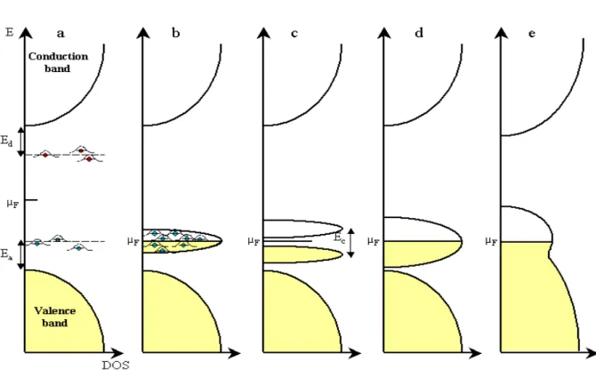
Box 2 : Metal-Insulator Transition
At T=0, semiconductors are insulators with their highest occupied electronic band and their lowest unoccupied electronic band of delocalized states separated by an energy bandgap with a chemical potential located at midgap. Randomly distributed chemical impurities or structural defects, leading to localized states within this forbidden gap, may liberate (donor centers) or capture (acceptor centers) electrons. At non-zero temperature, the number of free carriers in the bands will depend on the ratio of the ionization energy of these centers (respectively Ed and Ea) to the temperature, yielding an activated electrical
resistivity intermediate between that of an insulator and that of a metal (see fig. 2a).
In heavily doped semi-conductors, the impurity energy levels begin to aggregate into a narrow range of energy, a so-called “impurity band”, a misleading term since the wave-functions remain localized. Moreover, the dispersion of energy levels due to disorder contributes to the spatial localization of electronic states (Anderson localization). At higher concentration, when the impurities are close
enough, quantum overlapping of their wave-functions tends to delocalize them, leading to a metallic behavior at zero temperature with a Fermi level pinned inside the impurity band (see fig. 2b). Mott showed that this simplified one-electron picture fails, and that the conduction mechanism would remain thermally activated even if the impurities were regularly spaced[103]. Indeed, because of Coulomb repulsion, the spin degenerated half-filled impurity band splits into an empty band and a full band (see fig. 2c). Upon further doping, these two bands cross each other and the Metal-Insulator Transition (MIT) takes place (see fig. 2d).
However, at such doping levels, screening of the impurities modifiesy the ionization energy itself. Zero temperature model calculations have shown consequently that, at the transition, the impurity-band states associated withto the doping atoms become energetically unfavorable : upon adding one more impurity to the critical concentration, all these states become extended. Their energies now lie near the edge but within the band of delocalized states. Screening of the crystal host electrons by these new free carriers emphasizes this effect by narrowing the intrinsic bandgap energy[104] (see fig. 2e).
Fig. 2 : Evolution of the electronic density of states (DOS) and band structure with increasing p-type doping from a) to d). Colored area represents filled states.
Box 3 : Gas Immersion Laser Doping
Substitutional doping of semiconductors up to the alloying range is hampered by the solubility limit of the doping impurity into the host lattice. Above this limit the solid solution becomes thermodynamically unstable, leading to phase separation and formation of aggregates. Among the various out-of-equilibrium techniques developed to overcome this limitation, laser-assisted processes are well adapted to silicon, germanium, and their alloys. A laser burst melts the surface of the crystal during a few tens of nanoseconds. After the burst, the speed of re-crystallization is on the order of 1010 K/s, slow enough to allow crystal reconstruction on the underlying non melted template, but fast enough to prevent impurity diffusion and precipitation. Doping atoms can be introduced by pre-implantation (Laser Thermal Anneal or LTA) or in situ by exposure of the surface to impurity-carrying gas molecules in a vacuum chamber (Gas Immersion Laser Doping or GILD), as illustrated below.
Recently, the GILD technique has been applied to induce superconductivity in silicon by boron doping. In-situ real time monitoring of the transient reflectivity at a 675 nm wavelength allowed to adjust the power and duration of the pulses for optimal doping and to ensure that the dopant incorporation profile was flat with an abrupt interface. High-resolution XRD measurements and secondary ion mass spectroscopy on the doped layers demonstrated a maximum doping level of the order of 10% atomic (i.e. ~5.1021 at/cm3) for typically 500 subsequent laser shots. Note that this substitutional concentration is far above the critical threshold for the MIT (a few 1018 at/cm3) and even above the solubility limit (~1020 at/cm3). Unfortunately, this technique, well-adapted to silicon and germanium, can not be applied to most of the other semiconducting compounds (including diamond).
Step 1
Adsorption of boron onto the surface of the silicon wafer, schematized by horizontal atomic
planes.
Step 2
Local melting of silicon induced by the laser pulse. Boron diffuses
into the liquid.
Step 3
Recrystallization of silicon at the liquid-solid interface. Quench of boron into the
Acknowledgements
This work was partially funded by the French CNRS, CEA, and National Agency for Research (ANR) under contract ANR-05-BLAN-0282.
REFERENCES
[1] Nagamatsu, J., Nakagawa, N., Muranaka, T., Zenitani, Y. & Akimitsu, J. Superconductivity at 39 K in magnesium diboride. Nature 410, 63-64 (2001).
[2] Crespi, V.H. Superconductors: Clathrates join the covalent club. Nature Materials 2, 650 - 651 (2003).
[3] Ekimov, E.A., Sidorov, V.A., Bauer, E.D., Mel'nik, N.N., Curro, N.J., Thompson, J.D. & Stishov, S.M. Superconductivity in diamond. Nature 428, 542 - 545 (2004).
[4] Bustarret, E., Marcenat, C., Achatz, P., Ka1mar1ik, J., Lévy, F., Huxley, A., Ortéga, L., Bourgeois, E., Blase, X., Débarre, D. & Boulmer, J. Superconductivity in doped cubic silicon.
Nature 444, 465-468 (2006).
[5] Ren, Z.-A., Kato, J., Muranaka, T., Akimitsu, J., et al. Superconductivity in Boron-doped SiC,
J. Phys. Soc. Jap. 76, 103710 (2007).
[6] Kriener, M., Maeno, Y., Oguchi, T., Ren, Z.-A., et al. Specific heat and electronic states of superconducting boron-doped silicon carbide.Phys. Rev. B 78, 024517 (2008).
[7] Kawaji, H., Horie, H.-O., Yamanaka, S. & Ishikawa, M. Superconductivity in the Silicon Clathrate Compound (Na,Ba)xSi46 . Phys. Rev. Lett. 74, 1427-1429 (1995).
[8] Tanigaki, K., Shimizu, T., Itoh, K.M., Teraoka, J., Moritomo, Y. & Yamanaka, S. Mechanism of superconductivity in the polyhedral-network compound Ba8Si46. Nature Materials 2, 653-655
(2003).
[9] Hebard, A.F., Rosseinsky, M.J., Haddon, R.C., Murphy, D.W., Glarum, S.H., Palstra, T.T.M., Ramirez, A.P., Kortan, A.R., et al. Superconductivity at 18 K in Potassium-doped C60. Nature
350, 600-601 (1991).
[10] Varma, C.M., Zaanen, J. & Raghavachari, K. Superconductivity in the Fullerenes. Science
254, 989-992 (1991).
[11] Weller, T.E., Ellerby, M., Saxena, S.S., Smith, R.P. & Skipper, N.T. Superconductivity in the intercalated graphite compounds C6Yb and C6Ca. Nature Physics 1, 39 - 41 (2005).
[12] Emery, N., Hérold, C., d’Astuto, M., Garcia, V., Bellin, Ch., Marêché, J.F., Lagrange, P. & Loupias, G. Superconductivity of bulk CaC6. Phys. Rev. Lett. 95, 087003 (2005).
[13] Carbotte, J.P. Properties of boson exchange superconductors. Rev. Mod. Phys. 62, 1027-1157 (1990).
[14] Pickett, W.E. The next breakthrough in phonon-mediated superconductivity. Physica C 468, 126-135 (2008).
[15] Moussa, J.E. & Cohen, M.L. Constraints on TC for superconductivity in heavily boron-doped
diamond. Phys. Rev. B 77, 064518 (2008).
[16] Calandra, M. & Mauri, F. High-TC Superconductivity in Superhard Diamondlike BC5. Phys.
Rev. Lett. 101, 016401 (2008).
[17] Cava, R.J. Solid-state physics - Super Silicon. Nature 444, 427-428 (2006).
[18] Cohen, M.L. Superconductivity in many-valley semiconductors and in semimetals. Phys.
Rev. 134, A511-A521 (1964).
[19] Cohen, M.L. The existence of a superconducting state in semiconductors. Rev. Mod. Phys.
36, 240-243 (1964).
[20] Schooley, J.F., Hosler, W.R. & Cohen, M.L. Superconductivity in semiconducting SrTiO3.
Phys. Rev. Lett. 12, 474-475 (1964).
[21] Schooley, J.F., Hosler, W.R., Ambler, E., Becker, J.H., Cohen, M.L. & Koonce, C.S. Dependence of the Superconducting Transition Temperature on Carrier Concentration in Semiconducting SrTiO3. Phys. Rev. Lett. 14, 305-307 (1965).
[22] Hein, R.A., Gibson, J.W., Mazelsky, R., Miller, R.C. & Hulm, J.K. Superconductivity in Germanium Telluride. Phys. Rev. Lett. 12, 320-322 (1964).
[23] Gunnarsson, O. Superconductivity in fullerides. Rev. Mod. Phys. 69, 575-606 (1997).
[24] Iwasa, T. & Takenobu, T. Superconductivity, Mott-Hubbard states, and molecular orbital order in intercalated fullerides. Journal of Physics-Condensed Matter 15, R495-R519 (2003).
[25] Kasper, J.S., Hagenmuller, P., Pouchard, M. & Cros, C. Clathrate Structure of Silicon Na8Si46 and NaxSi136 (x < 11). Science 150, 1713–1714 (1965).
[26] Connétable, D., Timoshevskii, V., Masenelli, B., Beille, J., et al. Superconductivity in Doped sp3 Semiconductors: The Case of the Clathrates. Phys. Rev. Lett. 91, 247001 (2003). [27] Solozhenko, V.L., Dubrovinskaia, N.A. & Dubrovinsky, L.S. Synthesis of bulk superhard
semiconducting B–C material. Appl. Phys. Lett. 85, 1508-1510 (2004).
[28] Ekimov, E.A., Sadykov, R.A., Mel’nik, N.N., Presz, A., Tat’yanin, E.V., Slesarev, V.N. & Kuzin, N.N. Diamond crystallization in the system B4C-C. Inorg. Mater. 40, 932-936 (2004).
[29] Dubitskiy, G.A., Blank, V.D., Buga, S.G., Semenova, E.E., Kul’bachinskii, V.A., Krechetov, A.V. & Kytin, V.G. Superhard superconducting materials based on diamond and cubic boron nitride. JETP Lett. 81, 260-263 (2005).
[30] Dubrovinskaia, N., Dubrovinsky, L., Papageorgiou, T., Bosak, A., Krisch, M., Braun, H.F. & Wosnitza, J. Large carbon-isotope shift of TC in boron-doped diamond, Appl. Phys. Lett. 92,
132506 (2008).
[31] Takano, Y., Nagao, M., Sakaguchi, I., Tachiki, M., Hatano, T., Kobayashi, K., Umezawa, H. & Kawarada, H. Superconductivity in diamond thin films well above liquid helium temperature.
Appl. Phys. Lett. 85, 2851-2853 (2004).
[32] Bustarret, E., Ka1mar1ik, J., Marcenat, C., Gheeraert, E., Cytermann, C., Marcus, J. & Klein, T. Dependence of the Superconducting Transition Temperature on the Doping Level in Single-Crystalline Diamond Films. Phys. Rev. Lett. 93, 237005 (2004).
[33] Kato, Y., Matsui, F., Shimizu, T., Daimon, H., Matsushita, T., Guo, F.Z. & Tsuno, T. Dopant-site effect in superconducting diamond (111) studied by atomic stereophotography. Appl.
Phys. Lett. 91, 251914 (2007).
[34] H. Mukuda, H., T. Tsuchida, T., A. Harada, A., Y. Kitaoka, Y., T. Takenouchi, T., Y. Takano, Y., M. Nagao, M., et al., Microscopic evidence for evolution of superconductivity by effective carrier doping in boron-doped diamond: 11B-NMR study. Phys. Rev. B 75, 033301 (2007).
[35] Nesladek, M., Tromson, D., Mer, C., Bergonzo, P., Hubik, P. & Mares, J.J. Superconductive B-doped nanocrystalline diamond thin films: Electrical transport and Raman spectra. Appl. Phys.
Lett. 88, 232111 (2006).
[36] Ishizaka, K., Eguchi, R., Tsuda, S., Yokoya, T., Chainani, A., Kiss, T., Shimojima, T., Togashi, T., Watanabe, S., et al. Observation of a Superconducting Gap in Boron-Doped Diamond by Laser-Excited Photoemission Spectroscopy. Phys. Rev. Lett. 98, 047003 (2007). [37] Cammilleri, D., Fossart, F., Debarre, D., Tran Manh, C., Dubois, C., Bustarret, E., Marcenat, C., Achatz, P., Bouchier, D., Boulmer, J. Highly doped Si and Ge formed by GILD (gas immersion doping) ; from GILD to superconducting silicon. Thin Sol. Films 517, 75-79 (2008).
[38] Kortus, J. Superconductivity: where are the electrons. Nature Materials 4, 879-880 (2005). [39] Baskaran, G. Strongly correlated impurity band superconductivity in diamond : X-ray spectroscopic evidence. Sci. Technol. Adv. Materials 7, S49-S53 (2006); and references therein. [40] Capone, M., Fabrizio, M., Castellani, C. & Tosatti, E. Strongly correlated superconductivity.
[41] Han, J.E., Gunnarsson, O. & Crespi, V.H. Strong superconductivity with local Jahn-Teller phonons in C60 solids. Phys. Rev. Lett. 90, 167006 (2003).
[42] Boeri, L., Kortus, J. & Andersen, O.K. Three-dimensional MgB2-type superconductivity in
hole-doped diamond. Phys. Rev. Lett. 93, 237002 (2004).
[43] Lee, K.W. & Pickett, W.E. Superconductivity in boron-doped diamond. Phys. Rev. Lett. 93, 237003 (2004).
[44] Ma, Y., Tse, J.S., Cui, T., Klug, D.D., Zhang, L., Xie, Y., Niu, Y. & Zou, G. First-principles study of electron-phonon coupling in hole- and electron-doped diamonds in the virtual crystal approximation. Phys. Rev. B 72, 014306 (2005).
[45] Blase, X., Adessi, Ch. & Connétable, D. Role of the dopant in the superconductivity of diamond. Phys. Rev. Lett. 93, 237004 (2004).
[46] Xiang, H.J., Li, Z.Y., Yang, J.L., Hou, J.G. & Zhu, Q.S. Electron-phonon coupling in a boron-doped diamond superconductor. Phys. Rev. B 70, 212504 (2004).
[47] Giustino, F., Yates, J.R., Souza, I., Cohen, M.L. & Louie, S.G. Electron-Phonon Interaction via Electronic and Lattice Wannier Functions: Superconductivity in Boron-Doped Diamond Reexamined. Phys. Rev. Lett. 98, 047005 (2007).
[48] Bourgeois, E. & Blase, X. Superconductivity in doped cubic silicon: An ab initio study,
Appl. Phys. Lett. 90, 142511 (2007).
[49] Margine, E.R. & Blase, X. Ab initio study of electron-phonon coupling in boron-doped SiC.
Appl. Phys. Lett. 93, 192510 (2008)
[50] Lee, K.W. & Pickett, W.E. Boron spectral density and disorder broadening in B-doped diamond. Phys. Rev. B 73, 075105 (2006).
[51] Yokoya, T., Nakamura, T., Matsushita, T., Muro, T., Takano, Y., Nagao, M., Takenouchi, T., Kawarada, H. & Oguchi, T. Origin of the metallic properties of heavily boron-doped superconducting diamond. Nature 438, 647-50 (2005).
[52] Nakamura, J., Yamada, N., Kuroki, K., Oguchi, K.,Okada, K., Takano, Y., et al., Holes in the valence band of superconducting boron-doped diamond film studied by soft X-ray absorption and emission spectroscopy. J. Phys. Soc. Jap. 77, 054711 (2008).
[53] Migdal, A.B. Interactions between electrons and the lattice vibrations in a normal metal. Zh.
Eksp. Teor. Fiz. 34, 1438-1446 (1958) [Sov. Phys. JETP 7, 996 (1958)].
[54] Bardeen, J., Cooper, L.N. & Schrieffer, J.R. Microscopic theory of superconductivity. Phys.
[55] Sacépé, B., Chapelier, C., Marcenat, C., Ka1mar1ik, J., Klein, T., Bernard, M. & Bustarret, E. Tunneling Spectroscopy and Vortex Imaging in Boron-Doped Diamond. Phys. Rev. Lett. 96, 097006 (2006).
[56] Ekimov, E.A., Sidorov, V.A., Zoteev, A., Lebed, Yu. B., Thomson, J.D. & Stishov, S.M., Structure and superconductivity of isotope-enriched boron-doped diamond. Sci. Technol. Adv.
Materials 9, 044210 (2008).
[57] Carbotte, J.P., Greeson, M. & Perez-Gonzalez, A. Modification of the isotope effect due to pair breaking. Phys. Rev. Lett. 66, 1789-1792 (1991).
[58] Ishizaka, K., Eguchi, R., Tsuda, S., Chainani, A., et al. Temperature-dependent localized excitations of doped carriers in superconducting diamond. Phys. Rev. Lett. 100, 166402 (2008). [59] Hoesch, M., Fukuda, T., Mizuki, J., Takenouchi, T., Kawarada, H., Sutter, J.P., et al. Phonon softening in superconducting diamond. Phys. Rev. B 75, 140508 (2007).
[60] Ortolani, M., Lupi, S., Baldassarre, L., Schade, U., Calvani, P., Takano, Y., Nagao, M., Takenouchi, T. & Kawarada, H. Low-energy electrodynamics of superconducting diamond.
Phys. Rev. Lett. 97, 097002 (2006).
[61] P. Achatz, PhD thesis, Université Joseph Fourier, Grenoble, France (2008).
[62] Calandra, M., Vast, N. & Mauri, F. Superconductivity from doping boron icosahedra. Phys.
Rev. B 69, 224505 (2004).
[63] Solozhenko, V.L., et al. unpublished
[64] Zinin, P.V., Ming, L.C., Kudryashov, I., Konishi, N., Manghnani, M.H. & Sharma, S.K. Pressure- and temperature-induced phase transition in the B-C system. J. Appl. Phys. 100, 013516 (2006).
[65] Goss, J.P. & Briddon, P.R. Theory of boron aggregates in diamond: First-principles calculations. Phys. Rev. B 73, 085204 (2006).
[66] Bourgeois, E., Bustarret, E., Achatz, P., Omnès, F. & Blase, X. Impurity dimers in superconducting B-doped diamond: Experiment and first-principles calculations, Phys. Rev. B 74, 094509 (2006).
[67] Dubrovinskaia, N., Wirth, R., Wosnitza, J., Papageorgiou, T., Braun, H.F., Miyajima, N. & Dubrovinsky, L. An insight into what superconducts in polycrystalline boron-doped diamonds based on investigations of microstructure. PNAS 105, 11619-11622 (2008).
[68] Schluter, M., Lannoo, M., Needels, M. & Baraff, G.A. Electron-phonon coupling and superconductivity in alkali-intercalated C60 solid. Phys. Rev. Lett. 68, 526-529 (1992).
[69] Côté, M., Grossman, J.C., Cohen, M.L. & and Louie, S.G. Electron-Phonon Interactions in Solid C36. Phys. Rev. Lett. 81, 697-700 (1998).
[70] Breda, N., Broglia, R.A., Colò, G., Onida, G., Provasi, D. & Vigezzi, E. C28: A possible
room temperature organic superconductor, Phys. Rev. B 62, 130-133 (2000).
[71] Benedict, L.X., Crespi, V.H., Louie, S.G. & Cohen, M.L. Static conductivity and superconductivity of carbon nanotubes: Relations between tubes and sheets. Phys. Rev. B 52, 14935-14940 (1995).
[72] Kociak, M., Kasumov, A.Yu., Guéron, S., Reulet, B., Khodos, I.I., Gorbatov, Yu.B., Volkov, V.T., Vaccarini, L. & Bouchiat, H. Superconductivity in Ropes of Single-Walled Carbon Nanotubes. Phys. Rev. Lett. 86, 2416-2419 (2001).
[73] Tang, Z.K., Zhang, L.Y., Wang, N., Zhang, X.X., Wen, G.H., Li, G.D., Wang, J.N., Chan, C.T. & Sheng, P. Superconductivity in 4 Angstrom Single-Walled Carbon Nanotubes. Science
292, 2462-2465 (2001).
[74] Nunez-Regueiro, M., Marques, L., Hodeau, J.L., Bethoux, O. & Perroux, M. Polymerized Fullerite Structures. Phys. Rev. Lett. 74, 278-281 (1995).
[75] Blank, V., Popov, M., Pivovarov, G., Lvova, N., Gogolinsky, K. & Reshetov, V. Ultrahard and superhard phases of fullerite C-60: comparison with diamond on hardness and wear. Diam.
Rel. Mater. 7, 427-431 (1998).
[76] Blase, X., Gillet, P., San Miguel, A. & Mélinon, P. Exceptional Ideal Strength of Carbon Clathrates. Phys. Rev. Lett. 92, 215505 (2004).
[77] Devos, A. & Lannoo, M. Electron-phonon coupling for aromatic molecular crystals: Possible consequences for their superconductivity. Phys. Rev. B 58, 8236-8239 (1998).
[78] Park, C.-H., Giustino, F., Cohen, M.L. & Louie, S.G. Velocity Renormalization and Carrier Lifetime in Graphene from the Electron-Phonon Interaction. Phys. Rev. Lett. 99, 086804 (2007). [79] Calandra, M. & Mauri, F. Electron-phonon coupling and electron self-energy in electron-doped graphene: Calculation of angular resolved photoemission spectra. Phys. Rev. B 76, 205411 (2007).
[80] Mélinon, P., Kéghélian, P., Blase, X., Le Brusc, J. & Perez, A. Electronic signature of the pentagonal rings in silicon clathrate phases: Comparison with cluster-assembled films. Phys. Rev.
B 58, 12590 - 12593 (1998).
[81] Zipoli, F., Bernasconi, M. & Benedek, G. Electron-phonon coupling in halogen-doped carbon clathrates from first principles. Phys. Rev. B 74, 205408 (2006).
[82] Comeau, M., Leleyter, M., Leclercq, J. & Pascoli, G. Electronic structures and stabilities of MpCn microclusters. II. BpCn (n<6, p=1,3). AIP-Conference Proceedings 312, 605-611 (1994).
[83] Hach, C.T., Jones, L.E., Crossland, C. & Thrower, P.A. An investigation of vapour deposited boron-rich carbon - a novel graphite-like material. Part I. The structure of BCx/C6B thin
films. Carbon 37, 221-230 (1999).
[84] Liu, A.Y. & Mazin, I.I. Combining the advantages of superconducting MgB2 and CaC6 in
one material: Suggestions from first-principles calculations. Phys.Rev. B 75, 064510 (2007). [85] Calandra, M., Kolmogorov, A.N. & Curtarolo, S. Search for high TC in layered structures:
The case of LiB. Phys. Rev. B 75, 144506 (2007).
[86] Ribeiro, F.J. & Cohen, M.L. Possible superconductivity in hole-doped BC3. Phys. Rev. B 69,
212507 (2004).
[87] Rosner, H., Kitaigorodsky, A. & Pickett, W.E. Prediction of High TC Superconductivity in
Hole-Doped LiBC. Phys. Rev. Lett. 88, 127001 (2002).
[88] Moussa, J.E., Noffsinger, J. & Cohen, M.L. Possible thermodynamic stability and superconductivity of antifluorite Be2BxC1-x. Phys. Rev. B 78, 104506 (2008).
[89] Schäpers, T. Superconductor / Semiconductor junctions. Springer tracts in modern physics vol. 174, (2001).
[90] Doh, Y.-J., van Dam, J.A., Roest, A.L., Bakkers, E.P.A.M., Kouwenhoven, L.P. & De Franceschi, Tunable Supercurrent Through Semiconductor Nanowires, Science 309, 272-275 (2005).
[91] Takayanagi, H. & Kawakami, T. Superconducting Proximity Effect in the Native Inversion Layer on InAs. Phys. Rev. Lett. 54, 2449-2452 (1985).
[92] Ekinci, K.L. & Roukes, M.L., Nanoelectromechanical systems. Rev. Sci. Instrum. 76, 061101 (2005).
[93] Naik, A., Buu, O., LaHaye, M.D., Armour, A.D., Clerk, A.A., Blencowe, M.P. & Schwab, K.C. Cooling a nanomechanical resonator with quantum back-action. Nature 443, 193-196 (2006).
[94] Gaidarzhy, A., Imboden, M., Mohanty, P., Rankin, J. & Sheldon, B.W. High quality factor gigahertz frequencies in nanomechanical diamond resonators. Appl. Phys. Lett. 91, 203503 (2007).
[95] Lüders, M., Marques, M.A.L., Lathiotakis, N.N., Floris, A., Profeta, G., Fast, L., Continenza, A., Massidda, S. & Gross, E.K.U. Ab initio theory of superconductivity. I. Density functional formalism and approximate functionals. Phys Rev. B 72, 024545 (2005)
[96] Marques, M.A.L., Lüders, M., Lathiotakis, N.N., Profeta, G., Floris, A., Fast, L., Continenza, A., Gross, E.K.U. & Massidda, S. Ab initio theory of superconductivity. II. Application to elemental metals. Phys. Rev. B 72, 024546 (2005).
[97] Shirakawa, T., Horiuchi, S., Ohta, Y., & H. Fukuyama, H. Theoretical study on superconductivity in boron-doped diamond. J. Phys. Soc. Jap. 76, 014711 (2007).
[98] Yanase, Y. & Yorozu, N. Localization and superconductivity in doped semiconductors, cond-mat. 08102915
[99] Klein, T., Achatz, P., Ka1mar1ik, J., Marcenat, C., Gustafsson, F., Marcus, J., Bustarret, E., Pernot, J., Omnes, F., Sernelius, B., Persson, C., Ferreira da Silva, A. & Cytermann, C. Metal-insulator transition and superconductivity in boron-doped diamond. Phys. Rev. B 75, 165313 (2007).
[100] Feigel’man, M.V., Ioffe, L.B., Kravtsov, V.E. & and Yuzbashyan, E.A. Eigenfunction Fractality and Pseudogap State near the Superconductor-Insulator Transition. Phys. Rev. Lett. 98, 027001 (2007).
[101] Achatz, P., Pernot, J., Marcenat, C., Ka1mar1ik, J., Ferro, G. & Bustarret, E. Doping-induced metal-insulator transition in aluminum-doped 4H silicon carbide. Appl. Phys. Lett. 92, 072103 (2008).
[102] Débarre, D. & Boulmer, J. private communication.
[103] Mott, N.F. Metal-insulator transitions. Taylor & Francis Ltd, London, 1974
[104] Persson, C. & Ferreira da Silva, A. Electronic Properties of Intrinsic and Heavily Doped 3C-, nH-SiC (n=2,4,6) and II-N (III = B,Al,Ga,In) in : Optoelectronic Devices : III-Nitrides, Edited by M. Razeghi and M. Henini, Elsevier Advanced Technology, London , 2004.