HAL Id: hal-00272503
https://hal.archives-ouvertes.fr/hal-00272503
Submitted on 11 Dec 2014
HAL is a multi-disciplinary open access
archive for the deposit and dissemination of
sci-entific research documents, whether they are
pub-lished or not. The documents may come from
teaching and research institutions in France or
abroad, or from public or private research centers.
L’archive ouverte pluridisciplinaire HAL, est
destinée au dépôt et à la diffusion de documents
scientifiques de niveau recherche, publiés ou non,
émanant des établissements d’enseignement et de
recherche français ou étrangers, des laboratoires
publics ou privés.
Intrinsic electric fields in N-polarity GaN/AlxGa1-xN
quantum wells with inversion domains
Pierre Bigenwald, B Monemar, T. V. Shubina, A. A. Toropov, V. N. Jmerik,
M. G. Tkachman, A. V. Lebedev, V. V. Ratnikov, A. A. Sitnikova, V. A.
Vekshin, et al.
To cite this version:
Pierre Bigenwald, B Monemar, T. V. Shubina, A. A. Toropov, V. N. Jmerik, et al.. Intrinsic electric
fields in N-polarity GaN/AlxGa1-xN quantum wells with inversion domains. Physical Review B:
Condensed Matter and Materials Physics (1998-2015), American Physical Society, 2003, 67 (19),
pp.10. �10.1103/PhysRevB.67.195310�. �hal-00272503�
Intrinsic electric fields in N-polarity GaNÕAl
xGa
1ÀxN quantum wells with inversion domains
T. V. Shubina,*A. A. Toropov, V. N. Jmerik, M. G. Tkachman, A. V. Lebedev, V. V. Ratnikov, A. A. Sitnikova, V. A. Vekshin, S. V. Ivanov, and P. S. Kop’ev
Ioffe Physico-Technical Institute, Polytekhnicheskaya 26, St. Petersburg 194021, Russia
P. Bigenwald
LASMEA-UMR 6602 CNRS-UBP, 63177 Aubiere Cedex, France
J. P. Bergman, P. O. Holtz, and B. Monemar
Department of Physics and Measurement Technology, Linko¨ping University, S-581 83 Linko¨ping, Sweden
~Received 13 August 2002; revised manuscript received 12 November 2002; published 7 May 2003; publisher error corrected 8 May 2003!
GaN/AlGaN quantum wells ~QWs! of dominant N polarity with inversion domains ~IDs!, grown by molecular-beam epitaxy, have been studied. Two-band photoluminescence ~PL!, with the lower-energy band and an additional absorption edge related to the IDs, is observed in these QWs due to a difference in strain, electric field, and well width in the regions of different polarities. A time-resolved PL study reveals additionally strong inhomogeneity of the electric fields among the IDs. The intrinsic electric fields in the structures are relatively small—their maximal estimated value of 180 kV/cm is among the lowest ever reported. The low-scale electric fields indicate likely polarization deterioration in the N-polarity structures. These conditions are favorable for bright PL up to room temperature in 8 –9-nm-wide wells.
DOI: 10.1103/PhysRevB.67.195310 PACS number~s!: 78.47.1p, 78.66.Fd, 77.65.Ly, 81.07.St
I. INTRODUCTION
Recently it has been recognized that built-in electric fields induced by spontaneous polarization ~SP! and piezoelectric
~PE! effects in III-nitride-based quantum wells ~QWs! result
in a strongly decreased intensity and red energy shift of pho-toluminescence ~PL! due to the quantum-confined Stark effect.1–7. Most of the optical investigations of the phenom-enon have considered the QW structures as being structurally uniform, and SP and PE polarization as macroscopically ho-mogenous, although real samples usually contain many in-version domains ~IDs!. In these regions, 5–30 nm in diam-eter, the polarity is reversed with respect to the rest of the surface.8 –10The change of polarity takes place at ID bound-aries ~IDBs! lying usually within$1 –100% planes.
Until now there has been a lack of data concerning optical properties of the QWs with IDs, especially of N-polar ones, where the density of IDs may be rather high. These struc-tures are currently considered as poorly luminescent,11 al-though intense PL from N-polar GaN films has been reported recently.12The low formation energy of IDBs usually emerg-ing from the sapphire interface is a prerequisite for their propagation throughout the entire epilayer, including the QWs. One could expect a vertical stack of QWs inside the IDBs to exhibit optical properties differing from those of the remaining sample area. An imposed difference (;90 meV) in PL energies of the Ga- and N-polar GaN layers grown on a patterned AlN/c-Al2O3, as well as bright PL at their
boundaries, have been demonstrated, although not com-pletely explained.13
The switching of the polarity at an IDB means an instant sign change of the intrinsic electric fields. At a first glance these field fluctuations between positive and negative values are unessential for PL @in contrast to the effects related to a two-dimensional electron gas,14 ~2DEG!# since the absolute
value of the intrinsic field is to be the same in the regions of different polarities, and spatially oblique transitions occur between electrons and holes pushed out towards the opposite interfaces of QW and ID regions. However, the equivalence of the strain and electric fields in the IDs and the main area has not been proven so far.
In this paper, we report on ID manifestations in the optical properties of GaN/AlGaN QW structures of dominant N po-larity. Our findings demonstrate that a most intense PL band in the QW can be correlated with the IDs rather than with the main area. The results obtained also imply a strong decrease of the intrinsic electric fields in the N-polar QWs with the domains.
The paper is organized as follows. A detailed description of the samples studied is given in Sec. II, focusing on the polarity assignment, the appearance of the IDs and the real-ized strains. In Sec. III, we present the basic optical proper-ties of the structures directly related to the IDs. The pecu-liarities of the PL, elucidated by both cw and time-resolved
~TR! studies, are given in Sec. IV. Consideration of intrinsic
electric fields in the QWs with IDs is given in Sec. V. We compare the field, which is expected at different strain con-ditions determined by x-ray diffractometry ~XRD! ~Sec. V A! with the fields deduced from the optical experiments ~Sec. V B!. The latter fields are estimated considering conse-quences of the Stark effect on the optical properties. In the Sec. VI, we discuss the validity of our results and possible mechanisms of the electric-field decrease in the N-polar structures with IDs.
II. GROWTH, CHARACTERIZATION, AND POLARITY ASSIGNMENT
The structures studied were grown at 720 °C on ~0001! sapphire by plasma-assisted molecular-beam epitaxy ~MBE! PHYSICAL REVIEW B 67, 195310 ~2003!
using a radio frequency capacitively coupled magnetron.15 The growth was initiated directly by a high-temperature
1-mm-thick AlGaN layer with the AlN content ~x! of about 10% without any GaN buffer. The similar AlGaN cap layer of 120-nm thickness was grown on top of the QW active region. This permitted us to measure absorption in addition to reflection and both cw and TR PL. For a careful analysis of the interplay between the ID density and the optical prop-erties, we have chosen two representative samples. One of the structures contains three single QWs ~3-QW! of 8-, 5-, and 2.5-nm thickness, respectively, and the other is a mul-tiple quantum well ~MQW! sample with ten ;8-nm-thick QWs. The wells are separated by ;13-nm Al0.1Ga0.9N
bar-riers. The residual doping level in these structures is less than (125)31016 cm23 as determined by capacitance-voltage measurements.
The transition from the slightly (Ga/N;1) to strongly (Ga/N@1) Ga-rich growth regime took place between the center and the periphery of the samples due to a certain tem-perature gradient. This fact permitted us to vary the density of IDs across the wafer surface as reported previously.16The type of reflection high-energy electron-diffraction pattern monitored in situ during the growth was (131), and no (2
32) structure was observed. At temperatures below 300 °C,
we registered the (131)→(333) and (131)→(636) transitions in the regions grown at Ga/N;1 and Ga/N@1, respectively. Such reconstructions are typical for the N polarity.17
Scanning electron microscopy ~SEM! surface images taken at different spots on the samples using the CamScan S4-90 field-emission microscope demonstrate a smooth film surface at the periphery and a rough one in the center, filled by hillocks of a height of up to a few tens of nanometers, which is indicative of ID formation @Figs. 1~a! and 1~b!#.
Transmission-electron microscopy ~TEM! images also reveal plain and perfect QWs in the outer regions, while there are many IDs in the central area, originating from the interface with the substrate @Figs. 1~c! and 1~d!#. The cross-sectional TEM images were taken for g5(0002) using a Philips EM-420 microscope at a 100-kV voltage. The domains were eas-ily distinguished from other defects by imaging the same region at different diffraction conditions, e.g., varying g.18 The density of the IDs amounts to 431010cm2 in the center, and drops by an order of magnitude in the perfect interme-diate region grown at Ga/N.1. The periphery is almost free of IDs, but instead the density of nanopipes increases signifi-cantly there. The average widths of wells and barriers are found to be slightly larger in the center (lw59, lb 514 nm) than at the periphery (lw58, lb513 nm) as
deter-mined by a TEM study. This conclusion is verified by the determination of the MQW period via the angle separation between the interference fringes in the XRD scans measured at different points along the sample surface. The increase of the widths is obviously related to a higher growth rate at the numerous Ga-polar IDs.19,20
The strain conditions in the samples were studied by XRD using double- and triple-crystal diffractometers and Cu Ka1
radiation. The material parameters used for the strain and electric-field estimations presented below were taken from Refs. 21–24. The physical quantities of the AlxGa12xN al-loys were determined using Vegard’s law. The average in-plane stresses sa were determined with an accuracy of ;10% by the measurements of the curvature of the sapphire
substrate and the use of the Stoney equation, as described previously.25The samples have a complex convex shape with different radii in the ID-enriched and ID-free regions, which are 16.8 and 7.9 m in the MQW sample, and almost the same, 15.2 and 7.6 m, in the 3-QW sample. In the MQW sample, the radii correspond to compressive stresses of
21.3 and 22.8 GPa in the center and periphery,
respec-tively.
The values of macrostrain «calong the c axis and lateral
deformation «a are found using the well-known relations for a hexagonal structure: sa52(C/2C13)«c, «a 5(C/C33)/sa, where Ci j are elastic constants, and C 5(C111C12)C3322C13
2 . To find the Al content, we first
de-termined the exact interplanar spacing c in different regions, using a perfect 6H-SiC monocrystal as a reference, then found the average concentrations of Al via an equilibrium lattice constant c05c/(11«c). Different contents of Al in
the central ~0.085! and periphery ~0.118! regions provide dif-ferent misfits between the wells and the barrier (20.0020 and 20.0029, respectively!. The values of the lateral defor-mation of AlGaN layer, «a, obtained in both the center
(20.0027) and periphery (20.0058), show that a complete relaxation of the layer does not occur.
III. OPTICAL EVIDENCE OF INVERSION DOMAINS
In spite of the perfect morphology, the PL signal is neg-ligible at the periphery of the MQW and 3-QW samples, where the epilayers are almost free from the IDs but enriched by the nanopipes, while in the central parts of both samples, FIG. 1. SEM images taken from the surface of the GaN/AlGaN
MQW sample in the ~a! central and ~b! periphery regions grown under Ga/N;1 and Ga/N@1, respectively. Cross-sectional dark field TEM images are taken with g5(0002) from the ~c! central and ~d! periphery regions. Arrows mark the domain boundaries.
the PL is rather bright. For spots where the emission is strong, the PL spectra contain two bands separated by
;70–120 meV. The value of this energy separation depends
on the excitation power and the position on the samples. Figure 2~a! shows a PL spectrum with a strong lower-energy band and a weaker higher-energy one, taken in the central part of the MQW sample at low temperature ~10 K! and excitation by the 325-nm line of a 15-mW He-Cd laser. The emission from the AlGaN barriers, revealed at high excita-tion power as a shoulder near 3.72 eV, indicates that the two principal bands are related to the QW active region. In addi-tion, temperature-dependent measurements demonstrate that both bands in the MQW sample survive up to room tempera-ture @Fig. 3~a!#, which is rather characteristic for QW emissions.
Absorption spectra measured using a Xe lamp in the cen-ter of the MQW sample, enriched by the inversion domains
@Fig. 2~a!#, provide important information. In the spectral
region of the two-band PL emission, there is a prevailing absorption edge, which correlates well with the higher-energy band. ~The absorption edge of the AlGaN barrier ap-pears above 3.7 eV.! Moreover, an additional absorption edge was revealed as a shoulder at 3.52 eV, apparently related to the lower-energy emission. Since the domains occupy a sig-nificant part of the total area in the center, their density of states is sufficient to contribute to the absorption. Besides, the relatively high intensity of the higher-energy PL band can be realized, if the respective region occupies a significant part of the total area such as the main QW area of the domi-nant N polarity in our samples. Therefore, we tentatively attribute the lower- and higher-energy PL bands with the respective absorption features to the IDs and the main QW area, respectively.
A similar higher-energy PL band, previously observed in
GaN/AlGaN QWs, was explained in terms of spatially direct transitions within thick wells due to an extremely low carrier mobility.2However, some high-energy features are visible in the PL spectrum taken in the 3-QW sample @Fig. 2~b!#. One can assume that they due to two-band emission from each of the QWs of 2.5-, 5-, and 8-nm nominal widths. In the narrow wells, exciton radiative lifetimes are significantly less, which makes the explanation proposed in Ref. 2 incredible for our structures.
In the 3-QW samples, as well as in the MQWs, the lower-energy emission decreases faster with the temperature rise than the higher-energy one. As a result, we have registered three well-pronounced PL bands at high temperatures
@Fig. 3~b!#.
Figure 2~b! presents a reasonable variant of deconvolution of the complicated low-temperature PL spectrum in the 3-QW sample. It has been done using Gaussian contours because of the strain, thickness, and composition inhomoge-neities. The spectrum has been decomposed assuming two-band emission in each well. The lower-situated two-band in such emission originates at regions of intersections of QWs with IDs. Since the domains penetrate throughout the entire het-erostructure including every well, six peaks in total should be in the spectra of the 3-QW sample—three peaks from the main QW area and three more from such intersections. We believe that five peaks are seemingly in the spectrum, be-cause of close energies of two PL lines forming the middle doublet peak. Our estimation of exciton energies presented in Sec. V B, performed taking into account both strain and elec-tric field, has shown that such coincidence is possible. Thus, the well-separated peaks 1I and 2I are considered as the ID PL lines of 8- and 5-nm-wide wells, respectively. The middle peaks 3I and 1 are tentatively assigned to the ID PL in the 2.5-nm-wide QW and the basic QW PL in the 8-nm-wide QW, respectively. Peaks 2 and 3 are ascribed to emission from the main QW area in the 5- and 2.5-nm-wide wells, respectively.
To obtain the spectrum deconvolution the standard nonlinear-curve-fitting iterations are performed with some
FIG. 3. Photoluminescence spectra measured in ~a! the MQW sample and ~b! the 3-QW sample at various temperatures. The spec-tra are vertically shifted for clarity. The notation of the PL peaks is the same as in Fig. 2~b!.
FIG. 2. ~a! Photoluminescence ~solid line! and absorption
~dashed line! spectra measured in the central region of the MQW
sample. The arrows link PL bands related to IDs and a main QW area with the respective absorption edges. ~b! PL ~thick solid line! and reflection ~dashed line! spectra measured in the central part of the 3-QW sample. Thin solid lines represent the decomposition of the PL spectrum using six Gaussian contours. The arrows indicate PL peaks related to the main QW area ~1, 2, 3! and IDs (1I, 2I, 3I),
as well as reflection singularities (1R, 2R, 3R).
INTRINSIC ELECTRIC FIELDS IN N-POLARITY . . . PHYSICAL REVIEW B 67, 195310 ~2003!
reasonable limitations. First, we have estimated the high-energy limit for PL peak position in the narrowest QW by PL measurements at high excitation power, when the peak maxi-mum is most pronounced. The limit is about 3.64 eV, which permits us to neglect the higher-energy emission at the de-convolution. Second, during the first iteration we have fixed the widths of the well-separated peaks 1I and 2I. In the following iterations, the widths of the next peaks are estab-lished to be comparable to or more than the found values. In other words, various inhomogenieties at the N polarity are assumed to be similar to or more than those at the Ga one. This restriction instantly decreased the number of the pos-sible deconvolution variants. Allowable variation of the en-ergy positions of the peaks during the following iterations was within the 10-meV limit. Actually, only one uncertainty still remains, in assignment of the peaks 1 and 3I, and each
of those can be ascribed either to the ID PL of the 2.5-nm-wide well or to the basic PL of the 8-nm-2.5-nm-wide QW. There-fore, we consider the difference between the energies of the peaks as maximal inaccuracy in determination of their ener-gies. This inaccuracy, shown by vertical bars in Fig. 4, is taken into account in the estimation of the internal electric fields in Sec. V B.
A reflection spectrum monitored at the same region of the 3-QW sample exhibits no singularities in the spectral region of the 1Iand 2I ID-related lines, while pronounced reflection features marked as 1R, 2R, and 3Rin Fig. 2~b! correlate with the higher-energy part of the spectrum. The Stokes shifts of 20–25 meV between these reflection singularities and the emission peaks 1, 2, and 3 are close to the previously
re-ported value of 2265 meV for similar QWs,3while the gap between peaks 3I and 1R is larger (;36 meV). That impels us to assign, tentatively, the observed reflection feature to the main QW area. Therefore we plot the energy positions of the reflection singularities as related to the main QW PL bands in Fig. 4. The ID and QW PL peak energies registered in the MQW sample are shown there as well. One can see that the energies of ID PL in the wells of the 8-nm nominal width are close in both samples. The same concerns the respective QW PL peaks. This fact supports our assignment of the question-able peaks in the 3-QW sample.
Additional weighty arguments to assign the lower-energy PL emission to the IDs arise from both conventional PL and micro-PL (m-PL! measurements performed along the gradi-ent of the ID density. At them-PL study the laser beam was focused on the surface of the as-grown samples down to a diameter of 1.5mm, while the other conditions were similar to those reported in Ref. 26. These measurements demon-strated a quenching of the lower-energy bands, as compared with the higher-energy ones, with the ID density reduction. Typicalm-PL spectra along the ID gradient are presented in Fig. 5. One can see that the single ID PL band in the MQW sample and the triad of the ID PL peaks in the 3-QW sample are significantly weakened towards the periphery, which is consistent with the ID density decrease.
To finally confirm this model we have measured them-PL in the perfect region, grown at Ga/N.1, where the IDs are rare and tend to agglomerate. The accompanying hillocks are visible as smooth spots on the flat surface. Two spectra taken at the same conditions within such a spot and in close vicin-ity show a dramatic enhancement of the lower-energy band in the ID region, while the QW PL band dominates in the domain-free QW area ~Fig. 6!.
IV. PECULIARITIES OF THE TWO-BAND PHOTOLUMINESCENCE
A. cw measurements
Them-PL measurements reveal a complicated structure of the ID and QW bands. Besides the principal PL bands,
re-FIG. 4. Energies of higher- and lower-energy features in the 3-QW sample obtained from photoluminescence ~solid circles! and reflection ~stars! spectra. PL energies in the MQW samples are il-lustrated by open squares. Vertical bars present inaccuracy in deter-mination of the transition energies discussed in the text. When the bars are absent, this inaccuracy is within the limits of the marks. Calculated well-width dependencies of exciton energies are ob-tained at ~1! E520 kV/cm, Eg53.570 eV, «a520.0058; ~2! E
5120 kV/cm, Eg53.570 eV, «a520.0058; ~3! E5240 kV/cm,
Eg53.541 eV, «a520.0027; ~4! E5180 kV/cm, Eg53.504 eV,
«a50; ~5! E5390 kV/cm, Eg53.504 eV, «a50. Available data
on PL energies in similar QWs of Ga polarity are shown by open triangles ~Ref. 2!, diamonds ~Ref. 3!, crosses ~Ref. 6!, and circles
~Ref. 7!.
FIG. 5. The variation of microphotoluminescence spectra along a gradient of ID density in ~a! the MQW and ~b! 3-QW samples. The arrows indicate the evolution from enriched to ID-impoverished regions.
lated to the extended regions of opposite polarities, there are additional PL peaks situated between them. As shown by the measurements at a low excitation level, these peaks, espe-cially pronounced within the ID-enriched spots, originate from sharp narrow lines, whose detailed behavior and inter-pretation have been published elsewhere.27Note that similar lines were observed at the intentionally formed IDBs in a GaN film.13
The PL measurements performed at various excitation conditions ~Fig. 7! show that the QW and ID PL bands ex-hibit different behavior. The intensity of the higher-energy band increases more rapidly with power than that of the lower-energy one. The latter tends to saturate with the power increase, which is consistent with the attribution of the lower-energy band to the IDs occupying only a limited part of the total area.
The ID band is shifted by 30– 40 meV with increasing power, which is commonly assigned to the screening of the electric fields by excited carriers.1 On the contrary, the en-ergy position of the QW band is almost constant with the power. The different shifts imply disparate magnitudes of the intrinsic electric fields in the respective regions.
The temperature measurements demonstrate an emerging shoulder at 3.48 eV within the ID PL band at ;80 K ~Fig. 3!. The energy corresponds to the additional PL peak origi-nating from the sharp lines on the higher-energy wing of the ID band at high excitation power. Similar redistribution of intensity takes place within the basic QW band as well. Thus, one can assume that an increase of either temperature or excitation power involves higher states in the recombination process, whose origin needs additional study.
B. Time-resolved measurements
The temporal evolution of the two-band PL was studied by means of a streak camera for detection and sub-pico-second laser pulses for excitation. Selected PL spectra taken in the center of the MQW sample ~Fig. 8! demonstrate that the higher-energy band with a peak at 3.55 eV dominates within the first 100 ps of the PL decay. Subsequently, the ID-related band, which is initially of weaker intensity, due to a slower decay, gains in relative strength at longer delays.
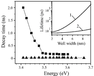
The fitting of the decay curves is performed using a two-exponential decay model except for the higher-energy wing of the QW band, where a single-exponential decay is ob-served. The characteristic decay times for the fast emission vary slightly ~30–70 ps! for two bands ~Fig. 9!. The same applies for the slow component of the higher-energy band
~130–220 ps!, while the decay times of the slow component
increase dramatically from 0.3 to 2–3 ns along the contour of the lower-energy band. This decay time variation can hardly be explained by the ;1 –2 monolayer QW widening within IDs revealed by the structural studies, since the latter could change the lifetimes by a factor of 2 to 3, maximum. On the contrary, local fluctuations of the electric field in the domains can disperse the values within an order of magnitude due to the dramatic reduction of the exciton oscillator strength with the field increase.2,5This finding evidences inhomogeneity of the array of the IDs, where important parameters such as the strain, electric fields, and sizes are fluctuating quantities.
We should highlight that a QW with IDs is a typical two-level system from the carrier kinetics point of view. Photo-created carriers move relatively freely in the plane of the QW and become trapped in the IDs. Besides the electric field, the
FIG. 6. Microphotoluminescence spectra measured at similar conditions in ~1! ID-enriched and ~2! ID-free spots in the MQW sample.
FIG. 7. Photoluminescence spectra measured in the center of the MQW sample at different excitations: ~1! the 325-nm line of a He-Cd laser, 50 W/cm2; ~2! the 337-nm line of a nitrogen pulse laser, 50 kW/cm2; and ~3! the 266-nm laser line, a micro-PL setup,
300 kW/cm2. The spectra are normalized to maximum intensities.
FIG. 8. Selected photoluminescence spectra registered at differ-ent delay times in the cdiffer-enter of the MQW sample.
INTRINSIC ELECTRIC FIELDS IN N-POLARITY . . . PHYSICAL REVIEW B 67, 195310 ~2003!
carrier kinetics is determinied by the generation rates in the IDs and the QW, the radiative and nonradiative recombina-tion lifetimes, and finally, by a transfer timettr
QW-ID between
the regions of different polarities, which depends essentially on the carrier mobility along the QW and the density of the IDs. If the transfer time is small enough, this enhances addi-tionally the fast decrease of the QW band intensity.
There are some experimental facts that seem to prove the two-level model. Namely, the energies of the peaks shift dif-ferently with the time. The QW PL band is redshifted, while the ID PL band is initially blueshifted followed by a redshift
@Fig. 10~a!#. The most significant shifts occur during the first
100 ps with a maximal increase of the ID PL intensity in that time domain @Fig. 10~b!#. During this time window, the car-rier transfer likely gives rise to screening of the built-in elec-tric field, causing the enhancement and blueshift of the ID
PL. When the flow of the nonequilibrium carriers exhausts, the blueshift is replaced by a redshift.
V. FLUCTUATION OF INTRINSIC ELECTRIC FIELDS A. Electric fields under different strain conditions
We have estimated the macroscopic intrinsic electric fields in the MQW structure, using the parameters obtained from the structural characterization ~see Sec. II!. The varia-tions of well and barrier thicknesses and Al content from the center (lw59, lb514 nm, x50.085) to periphery (lw58, lb513 nm, x50.118) were taken into account. In this
esti-mation, we neglect the possible fluctuation of the parameters around their average value.
The electric field is considered as the sum of the compo-nents induced by the piezoelectric (EPE) and spontaneous (ES P) polarizations:1,28 EwPE(S P)5 Pb PE(S P) 2 Pw PE(S P) k0@kw1kb• ~ lw/lb!# ,
EbPE(S P)52EwPE(S P)• ~ lw/lb!. ~1!
The indices w and b refer to the wells and the barriers,
PPE(S P) is the piezoelectric ~spontaneous! polarization,k0 is
the permittivity of the vacuum, kw(b) is the static dielectric
constant of the well ~barrier! material, and lw(b)is the
thick-ness of the well ~barrier!. Such a consideration neglects the possible contribution induced by the polarization in the thick AlGaN buffer that introduces a dominant error. It underesti-mates the electric fields in the wells and vice versa in the barriers. However, some saturation and disturbance of the polarization by defects in the thick layers can reduce the influence of this factor.29
The piezoelectric polarization along the c axis is PPE
52«a@e312e33(C13/C33)#, where «a is a lateral strain in a
layer, ei j are piezoelectric constants, and Ci j elastic
con-stants. The value of PPEis positive ~negative! for a compres-sive ~tensile! stress for the Ga polarity, while the spontaneous polarization is negative. ~The signs are reversed for the N polarity.! As a result, the spontaneous and piezoelectric po-larizations are antiparallel ~parallel! at compressive ~tensile! stress.1,14
However, the built-in electric fields induced by the PPE and PS P in the GaN QWs grown in an AlGaN matrix can have either the same or opposite signs, depending on the strain conditions. Indeed, for Ga polarity, the ( PbS P2 PwS P) and, hence, ES P are negative. In turn, the sign of the piezo-electric field is mostly determined by the difference in the lateral strains «a(b)2«a(w) in the barriers and wells. The
strained QWs are under additional misfit-induced compres-sion and the difference is negative. As a result, the magnitude of the electric field in the QWs, being a sum of the compo-nents, is maximal. In the MQW sample, it is estimated to be 470 kV/cm in the center and 640 kV/cm at the periphery. It is worth noting that the electric fields depend strongly on the choice of the SP parameters. A possible SP nonlinearity22can provide lowering of the resultant fields down to 220 and 300 kV/cm at the center and periphery, respectively.
FIG. 9. Variation of ~triangles! ‘‘fast’’ and ~squares! ‘‘slow’’ de-cay times along a contour of photoluminescence in the MQW sample. The inset presents calculated dependencies of the exciton radiative lifetimes on the well width with ~1! E5180 kV/cm, Eg
53.504 eV, «a50; ~2! E520 kV/cm, Eg53.570 eV, «a
520.0058.
FIG. 10. The ~a! energy shift and ~b! intensity variations of the
A mutual compensation due to different signs of the SP and PE polarization components is realized when the QWs are relaxed with respect to the strained barriers. This can decrease the intrinsic electric field from 470 to 150 kV/cm in the center, and even down to 60 kV/cm at the periphery. A joint relaxation of the wells and barriers disturbs the balance and worsens the compensation. In the limit case of full re-laxation of both the wells and barriers, the electric field var-ies in the range 80–340 kV/cm depending on the nonlinear-ity of the SP.
B. Stark effect in quantum wells with IDs
To estimate the electric fields realized in the regions of different polarities and the range of their fluctuation between the IDs and the rest of the QW area, we have performed fitting of the well-width dependencies obtained from the op-tical measurements ~see Fig. 4!. These dependencies, in ac-cordance with compressive strain revealed by XRD, are characterized by higher photon energies than published pre-viously for Ga-polarity GaN/AlGaN QWs. In addition, the dependencies are more flat, evidencing the weaker Stark effect.
The exciton energies in the AlGaN/GaN QWs were esti-mated within the envelope wave-function approximation, us-ing a variational approach with a sus-ingle-parameter varia-tional function for a quasi-two-dimensional exciton. The ratio of the conduction- and valence-band discontinuities is taken as 0.75/0.25,30and the carrier effective masses for AlN and GaN are taken from Ref. 31. For bulk GaN, the A exci-ton energy is determined as EA53.478115.4«c, where «cis
the strain along the c axis.32 The exciton binding energy is taken as 26 meV, and the AlN band gap as 6.23 eV.33For this calculation, the value of the fields in barriers is assumed to be 90 kV/cm.
In this calculation, we assumed for the main QW area in the MQW sample the values of the well and barrier thick-nesses and Al content determined for the periphery region, since the latter is almost ID-free. For the IDs we assumed the average values of the parameters characteristic for the central part enriched by the domains. We implied the same values for the well of 8-nm nominal width in the respective regions of the 3-QW samples and a proportional width variation for the narrower wells. Generally, in the ID regions the thick-nesses may be larger and the Al content can be less than their average values due to higher growth rate and suppressed in-corporation of Al, respectively. However, these fluctuations counteract with an influence on the transition energy, which can work in opposite directions, e.g., a 20–30-meV redshift due to an unaccounted ;1-nm well-width increase can be completely compensated by the blueshift due to a possible
;1% Al decrease.
The best fit of the ID-related well-width dependence is obtained assuming complete relaxation of both the GaN and AlGaN layers at the electric field of 180–200 kV/cm. One can see that fitting with the average strain measured by XRD in the center and the mean-field value of 240 kV/cm ~Fig. 4, dashed line! is much worse. Therefore, we speculate that some strain relaxation inside the IDs is possible, especially
taking into account that their formation is partly a response to the lattice mismatch at a sapphire/epilayer interface.
The dependence attributed to the main QW area is fitted to the strain conditions prevailing at the periphery area. The best fitting is obtained for an electric field not exceeding 20 kV/cm, in spite of the large compressive stress and absence of apparent QW relaxation ~e.g., in the TEM images!, which could cause a reduction of the field due to some compensa-tion of the SP and PE components. Note that the available data on well-width dependencies in Ga-polarity GaN/AlGaN QWs, unstrained due to the growth on thick GaN buffers,3–7 are fitted using the electric field of 390 kV/cm.
It should be emphasized that some error in the determina-tion of the electric fields can certainly arise from inaccuracy in the processing of the PL and reflection data. The above-discussed uncertainty in the assignment of the middle PL peaks in the 3-QW spectra can increase the field values up to 120 kV/cm in the N-polarity regions ~see Fig. 4, line 2!. In addition, the QW PL band has a complicated shape appar-ently consisting of two peaks in the ID-rich regions, which is probably related to carrier localization on IDBs. Our model does not consider that, nor a complexity of the lower-energy band. However, even taking the uncertainties into account, the intrinsic electric fields in the N-polar QW can hardly exceed 150 kV/cm.
We have used the values of 180 and 20 kV/cm to calculate the exciton radiative lifetimes ~see the inset of Fig. 9!. The so-obtained values are close to the experimental ones char-acteristic for an 8-nm-width QW. They are about 1 ns and 20 ps for 180 and 20 kV/cm2, respectively. The increase in the experimental decay time up to 220 ps within the lower-energy part of the QW band can be induced by carrier local-ization at the IDBs and other imperfections.
The electric fields can also be estimated via the PL energy shift from the center to the periphery, which is determined by the conjoint action of the strain ~blueshift! and the Stark effect ~redshift!. The observed ID PL redshift of ;10 meV is reasonable for a small variation of the intrinsic electric fields, e.g., due to the remnant strain. On the contrary, the PL in the strained QW area is not redshifted at all, but rather intensity redistribution between constituents takes place. Conse-quently, the Stark redshift is equal or less in magnitude com-pared to the anticipated strain-induced shift of 30 meV. Ac-cording to our estimation, this situation may be realized only at the small-scale electric fields.
VI. DISCUSSION
Our studies have exhibited that a difference in strain con-ditions and electric-field magnitudes together with well-width variation in N- and Ga-polarity regions in GaN/AlGaN QWs splits the PL emission into two bands and gives an additional absorption edge. The factors determining energies of the optical transitions are mutually dependent. For in-stance, the lower strain provides a higher growth rate.34That results in a local increase of well and barrier widths in the IDs, as compared to the surrounding area, accompanied by the respective variation of the electric fields.
The intrinsic electric fields in the Ga-polar regions of our INTRINSIC ELECTRIC FIELDS IN N-POLARITY . . . PHYSICAL REVIEW B 67, 195310 ~2003!
structures, as derived from a fitting of the well-width depen-dencies, is about a factor-of-2 less than what is convention-ally reported for similar GaN/AlGaN QWs of dominant Ga polarity.3,6Moreover, the value of internal electric field in the N-polarity regions ~the main QW area! of our structures is even smaller. It is important that such a dissimilarity between the electric-field values in regions of N and Ga polarities is realized inside the same structure with similar overall char-acteristics, such as the residual doping level.
Generally, the electric-field values in GaN/AlGaN QWs deduced from optical experiments are smaller than the theo-retically predicted ones. In the first papers considering inter-nal electric fields,2,28 only the piezoelectric component was taken into account. Nevertheless, in the validity limits of PE parameters used, a satisfactory agreement with the experi-mental results was achieved. In 1997 Bernardini et al. pointed out that the spontaneous as well as the piezoelectric polarizations are essentials of wurtzite nitrides which are non-centro-symmetric crystals with a polar axis.35They cal-culated the SP and PE parameters for these compounds that permitted consideration of both effects in the later studies. However, most of the following experimental papers have reported on an overestimation of the electric fields calculated using the theoretical parameters, as compared with those de-rived from the Stark shift.3,6,36 –38Leroux et al.3have deter-mined an internal field of 450 kV/cm in the QWs instead of the expected 620–750 kV/cm. Subsequent refining of the model parameters by consideration of nonlinearity of the po-larizations on the strain and the microscopic structure22 has allowed significantly better agreement between the experi-mental and theoretical results. Note that the nonlinearity of both the macroscopic polarizations has been directly demon-strated by means of observation of the internal field in the structures without noticeable strain39and pressure-dependent optical studies.40,41Besides the nonlinearity, different factors have been considered to explain the discrepancy between the theoretical and experimental data, such as the diminishing of the polarizations in the presence of defects3,42and screening of the internal fields by excited or residual carriers.2,5,43The carrier distribution inside a structure and the influence of surface barrier potential have been taken into account.42,44,45 The importance of the nonradiative recombination which controls the density of the photoexcited carriers and, hence, screening of the internal electric fields has been recognized as well.7,46
For our investigated structures, the possible influence of a varying depletion field across the wells as well as other ef-fects related to the residual doping42,44,45 can be neglected, because the level of the background doping is very low ~less than 531016 cm23). The electric-field screening by
photo-excited carriers, revealing itself as a blueshift of the PL emis-sion, exists in the Ga-polar regions but is absent in N-polar areas. The monitored shift corresponds to a deviation of about 50 kV/cm in this experimental determination of the field in comparison with theoretical predictions. On the con-trary, the nonlinearity of the polarization parameters can pro-vide a field lowering up to 220 kV/cm, which is comparable with the calculated value of 180–200 kV/cm for the Ga-polar regions. The enhanced stress and higher Al content in the
N-polar QWs area ought to increase the internal field. The nonradiative recombination times should be infinitely long7 to provide such flat well-width dependence, which is not realistic. Thus, when taking into account the respective nonlinearity47one could expect a field of about 300 kV/cm, i.e., significantly greater than the experimentally determined field.
The optical properties of the ID and QW regions agree with the estimated magnitudes of the intrinsic electric fields. The PL from the IDs is typical for an inhomogeneous array of localization sites under moderate fields. The Stokes shift between the ID PL and the respective absorption edge is rather large, about 60– 80 meV. The TR PL data show a dramatic increase of the characteristic decay times along a contour of the PL spectrum. The higher-energy PL band, on the other hand, demonstrates the behavior representative for a QW under a uniform electric field of a small magnitude. The characteristic decay times vary slightly along the QW PL contour. The peak energy does not change at an excitation power increase. The Stokes shift between the absorption edge and the PL is small (;20 meV).
The most important facts about the QW PL are the fol-lowing:
~i! The PL in the 8-nm-wide wells appears at a high
en-ergy (;3.6 eV) determined by strain. No noticeable Stark shift takes place in these wells.
~ii! The QW PL is enhanced in the ID-free regions, where
the ID-related PL components are weakened, as demon-strated by the m-PL study.
The latter fact proves our assignment of the higher-energy PL as originating from the main QW area, while the former facts confirm a small-scale electric field. Accordingly, all our results evidence an unexpectedly low intrinsic electric field in the N-polar QWs. It should be mentioned that some re-duction of the inherent polarizations can be expected in structures of mixed polarity, where the polarization-induced sheet charges of opposite signs along the same interface tend to compensate each other.14 However this overall effect has to diminish the field in regions of any polarity, being even less important in the extended N-polar ones. Whereas the field decrease in the Ga-polar relaxed IDs, in addition to what has been discussed above, could be caused by a set of factors, such as mutual compensation of the SP and PE com-ponents or crystal disturbances near IDBs, the reduction of the field in the strained and perfect QW area ~see Fig. 1! is possible only due to inherent deterioration of the spontane-ous polarization at the N polarity.
This assumption can hardly revise the model macroscopic polarization parameters which should be equal for either of the polarities. However, it is worth recalling that the sponta-neous polarization is a symmetry-dependent characteristic and any disturbance of the local crystal structure has to de-stroy it. The detailed analysis of the phenomenon is beyond the scope of the paper. Nevertheless, deteriorated structural properties of the N-polar layers as compared with the Ga-polar ones are well known. For instance, sheet carrier con-centration and 2-DEG mobility are smaller in N-polar GaN/ AlGaN heterostructures.48 The etching rate in N-polar structures is higher, reflecting the weaker bond strength, and
the PL intensity is usually less than that in Ga-polar structures.9@Strong emission observed in the N-polarity GaN ~Ref. 12! can be related to the Ga-polarity IDs, as
demon-strated by this study.# The worse structural properties might be accompanied by carrier localization in potential minima related to structural imperfections. That can enhance the non-radiative recombination times and, hence, facilitate the field screening.
However, if the field in the N-polar QW is not strong, the question of why QW PL intensity decreases so dramatically at the periphery arises. The ID density is reduced there, and the carrier transport to distant IDs is hampered. Our m-PL study reveals a PL drop to zero near the nanopipes whose PL density is rather high at the periphery. The nanopipes are predicted to be nonradiative centers.19 In regions free from these defects, the PL, being weaker by a factor of 1.5 to 2 than in the Ga-polar regions ~Fig. 6!, is intense enough to survive up to room temperature in accordance with the small magnitudes of the estimated electric fields.
In conclusion, QW structures with inversion domains give a unique opportunity to study optical properties in regions of opposite polarities grown at the same conditions. In the GaN/ AlGaN QWs grown by MBE, these regions are characterized by different strains and intrinsic electric fields. In addition, a dispersion of the electric fields among the IDs is established. Small-scale electric fields prevailing in the N-polarity struc-tures, related presumably to spontaneous polarization dete-rioration, provide bright photoluminescence even in the 8 –9-nm-wide wells.
ACKNOWLEDGMENTS
The authors thank Professor A. Kavokin for fruitful dis-cussions and R. V. Zolotareva and V. M. Busov for assistance in structural characterizations. This work was partly sup-ported by the RFBR Grant No. 03-02-17563, CLERMONT Project No. HPRN-CT-1999-00132, and the cooperative Grant between Russia and France, No. N04509PB.
*Electronic address: shubina@beam.ioffe.ru
1
V. Fiorentini, F. Bernardini, F. Della Sala, A. Di Carlo, and P. Lugli, Phys. Rev. B 60, 8849 ~1999!.
2J. S. Im, H. Kollmer, J. Off, A. Sohmer, F. Scholz, and A.
Hangle-iter, Phys. Rev. B 57, R9435 ~1997!.
3M. Leroux, N. Grandjean, M. Laugt, J. Massies, B. Gil, P.
Le-febvre, and P. Bigenwald, Phys. Rev. B 58, R13371 ~1998!.
4B. Gil, P. Lefebvre, J. Alle`gre, H. Mathieu, N. Grandjean, M.
Leroux, J. Massies, P. Bigenwald, and P. Christol, Phys. Rev. B
59, 10246 ~1999!.
5P. Lefebvre, J. Alle`gre, B. Gil, H. Mathieu, N. Grandjean, M.
Leroux, J. Massies, and P. Bigenwald, Phys. Rev. B 59, 15363
~1999!.
6N. Grandjean, B. Damilano, J. Massies, G. Neu, M. Tiessere, I.
Grzegory, S. Porowski, M. Gallart, P. Lefebvre, B. Gil, and M. Albrecht, J. Appl. Phys. 88, 183 ~2000!; P. A. Shields, R. J. Nicholas, N. Grandjean, and J. Massies, Phys. Rev. B 63, 245319 ~2001!.
7A. Di Carlo, A. Reale, P. Lugli, G. Traetta, M. Lomascolo, A.
Passaseo, R. Cingolani, A. Bonfiglio, M. Berti, E. Napolitani, M. Natali, S. K. Sinha, A. V. Drigo, A. Vinattieri, and M. Colocci, Phys. Rev. B 63, 235305 ~2001!.
8S. Ruvimov, in III-Nitride Semiconductors: Electrical, Structural
and Defects Properties, edited by O. Manasreh ~Elsevier,
Am-sterdam, 2000!.
9E. S. Hellman, MRS Internet J. Nitride Semicond. Res. 3, 11
~1998!.
10J. E. Northrup, J. Neugebauer, and L. T. Romano, Phys. Rev. Lett.
77, 103 ~1996!.
11S. F. Chichibu, A. Setoguchi, A. Uedoto, K. Yoshimura, and M.
Sumia, Appl. Phys. Lett. 78, 28 ~2001!.
12D. Huang, P. Visconti, M. A. Reshchnikov, F. Yun, T. King, A. A.
Baski, C. W. Litton, J. Jasinsli, Z. Liliental-Weber, and H. Mar-coc¸, Phys. Status Solidi A 188, 571 ~2001!.
13
P. J. Schuck, M. D. Mason, R. D. Grober, O. Ambacher, A. P. Lima, C. Miskys, R. Dimitrov, and M. Stutzmann, Appl. Phys. Lett. 79, 952 ~2001!.
14O. Ambacher, B. Foutz, J. Smart, J. R. Shealy, N. G. Weimann, K.
Chu, M. Murphy, A. J. Sierakowski, W. J. Schaff, L. F. Eastman, R. Dimitrov, A. Mitchell, and M. Stutzmann, J. Appl. Phys. 87, 334 ~2000!.
15V. N. Jmerik, V. V. Mamutin, V. A. Vekshin, T. V. Shubina, S. V.
Ivanov, and P. S. Kop’ev, Mater. Sci. Eng., B 59, 60 ~1999!.
16L. T. Romano and T. H. Meyers, Appl. Phys. Lett. 71, 3486
~1997!; T. H. Meyers, L. S. Hirsch, L. T. Romano, and M. R.
Richards-Babb, J. Vac. Sci. Technol. B 16, 2261 ~1998!.
17A. R. Smith, R. M. Feenstra, D. W. Greve, J. Neugebauer, and J.
E. Northrup, Appl. Phys. Lett. 72, 2114 ~1998!.
18V. Potin, P. Ruterana, and G. Nouet, J. Appl. Phys. 82, 2176
~1997!.
19Z. Liliental-Weber, Y. Chen, S. Ruvimov, and J. Washburn, Phys.
Rev. Lett. 79, 2835 ~1997!.
20K. M. Jones, P. Visconti, F. Yun, A. A. Baski, and H. Marcoc¸,
Appl. Phys. Lett. 78, 2497 ~2001!.
21F. Bernardini, V. Fiorentini, and D. Vanderbilt, Phys. Rev. B 63,
193201 ~2001!.
22F. Bernardini and V. Fiorentini, Phys. Rev. B 64, 085207 ~2001!. 23K. Kim, W. R. L. Lambrecht, and B. Segall, Phys. Rev. B 53,
16310 ~1996!.
24V. W. L. Chin, T. L. Tansley, and T. Osotchan, J. Appl. Phys. 75,
7365 ~1994!.
25V. Ratnikov, R. Kyutt, T. Shubina, T. Paskova, E. Valcheva, and
B. Monemar, J. Appl. Phys. 88, 6252 ~2000!.
26T. V. Shubina, T. Paskova, A. A. Toropov, S. V. Ivanov, and B.
Monemar, Phys. Rev. B 65, 075212 ~2002!.
27T. V. Shubina, V. N. Jmerik, M. G. Tkachman, V. A. Vekshin, V.
V. Ratnikov, A. A. Toropov, A. A. Sitnikova, S. V. Ivanov, J. P. Bergman, K. F. Karlsson, P. O. Holtz, and B. Monemar, Phys. Status Solidi B 234, 919 ~2002!; T. V. Shubina, V. N. Jmerik, M. G. Tkachman, V. A. Vekshin, A. A. Toropov, S. V. Ivanov, P. S. Kop’ev, J. P. Bergman, K. F. Karlsson, P. O. Holtz, and B. Mon-emar, Phys. Status Solidi A 195, 537 ~2003!.
28
A. D. Bykhovski, B. L. Gelmont, and M. S. Shur, J. Appl. Phys.
81, 6332 ~1997!.
29L. D. Landau and E. M. Lifshitz, Electrodinamika Sploshnyh Sred
~Nauka, Moskow, 1982! ~in Russian!, Vol. VIII @English
trans-INTRINSIC ELECTRIC FIELDS IN N-POLARITY . . . PHYSICAL REVIEW B 67, 195310 ~2003!
lation: L. D. Landau and E. M. Lifshitz, Electrodynamics of
Continuous Media ~Pergamon, Oxford, 1984!#.
30G. Martin, A. Botchkarev, A. Rockett, and H. Morkoc¸, Appl.
Phys. Lett. 68, 2541 ~1996!.
31K. Kim, W. R. L. Lambrecht, B. Segall, and M. van Schilfgaarde,
Phys. Rev. B 56, 7363 ~1997!.
32A. Shikanai, T. Azuhata, T. Sota, S. Chichibu, A. Kuramata, K.
Horino, and S. Nakamura, J. Appl. Phys. 81, 417 ~1997!.
33I. Vurgaftman, J. R. Meyer, and L. R. Ram-Mohan, J. Appl. Phys.
89, 5815 ~2001!.
34S. Ivanov and P. Kop’ev, in Antimonide-Related Strained-Layer
Heterostructures, edited by M. O. Manasreh, in Optoelectronic Properties of Semiconductors and Superlattices ~Gordon and
Breach, Amsterdam, 1997!, Vol. 3, pp. 95–170.
35F. Bernardini, V. Fiorentini, and D. Vanderbilt, Phys. Rev. B 56,
R10024 ~1997!.
36N. Grandjean, J. Massies, and M. Leroux, Appl. Phys. Lett. 74,
2361 ~1999!.
37N. Suzuki and N. Iizuka, Jpn. J. Appl. Phys., Part 2 38, L363
~1999!.
38S. H. Park and S. L. Chuang, Appl. Phys. Lett. 76, 1981 ~2000!. 39A. Bonfiglio, M. Lomascolo, G. Traetta, R. Cingolani, A. Di
Carlo, F. Della Sala, P. Lugli, A. Botchkarev, and H. Morkoc¸, J.
Appl. Phys. 87, 2289 ~2000!.
40G. Vaschenko, D. Patel, C. S. Menoni, H. M. Ng, and A. Y. Cho,
Appl. Phys. Lett. 80, 4211 ~2002!.
41P. Perlin, T. Suski, S. P. Lepkowski, H. Teisseyre, N. Grandjean,
and J. Massies, Phys. Status Solidi A 188, 839 ~2001!.
42G. H. Gainer, Y. H. Kwon, J. B. Lam, S. Bidnyk, A. Kalashyan, J.
J. Song, S. C. Choi, and G. M. Yang, Appl. Phys. Lett. 78, 3890
~2001!.
43R. Cingolani, A. Botchkarev, H. Tang, H. Morkoc¸, G. Traetta, G.
Coli, M. Lomascolo, A. Di Carlo, F. Della Sala, and P. Lugli, Phys. Rev. B 61, 2711 ~2000!.
44J. L. Sa´nchez-Rojas, J. A. Garrido, and E. Mun˜oz, Phys. Rev. B
61, 2773 ~2000!.
45J. Simon, R. Langer, A. Barski, M. Zervos, and N. T. Pelekanos,
Phys. Status Solidi A 188, 867 ~2001!.
46E.-J. Shin, J. Li, J. Y. Lin, and H. X. Jiang, Appl. Phys. Lett. 77,
1170 ~2000!.
47V. Fiorentini, F. Bernardini, and O. Ambacher, Appl. Phys. Lett.
80, 1204 ~2002!.
48R. Dimitrov, M. Murphy, J. Smart, W. Schaff, J. R. Shealy, L. F.
Eastman, O. Ambacher, and M. Stutzmann, J. Appl. Phys. 87, 3375 ~2000!.