HAL Id: hal-01232634
https://hal.archives-ouvertes.fr/hal-01232634
Submitted on 11 Mar 2020
HAL is a multi-disciplinary open access
archive for the deposit and dissemination of
sci-entific research documents, whether they are
pub-lished or not. The documents may come from
teaching and research institutions in France or
abroad, or from public or private research centers.
L’archive ouverte pluridisciplinaire HAL, est
destinée au dépôt et à la diffusion de documents
scientifiques de niveau recherche, publiés ou non,
émanant des établissements d’enseignement et de
recherche français ou étrangers, des laboratoires
publics ou privés.
Gwenaelle Hamon, Romain Cariou, Raphaël Lachaume, Jean Decobert, Kevin
Louarn, Wanghua Chen, J Alvarez, Jean-Paul Kleider, Pere Roca I.
Cabarrocas
To cite this version:
Gwenaelle Hamon, Romain Cariou, Raphaël Lachaume, Jean Decobert, Kevin Louarn, et al..
Inves-tigation of Hybrid Tunnel Junction Architectures for III-V/Si Tandem Solar Cells. 31st European
Photovoltaic Solar Energy Conference and Exhibition (EU-PVSEC 2015), Sep 2015, Hamburg,
Ger-many. pp.75-79, �10.4229/EUPVSEC20152015-1CO.10.4�. �hal-01232634�
INVESTIGATION OF HYBRID TUNNEL JUNCTION ARCHITECTURES FOR III-V/SI TANDEM SOLAR CELLS
G. Hamona,b, R. Carioub, R. Lachaumed, J. Decobertc, K. Louarnc, W. Chenb, J. Alvarezd, J.P. Kleiderd and P. Roca i Cabarrocasb
a Total MS – Energie Nouvelles - 24 cours Michelet, La Défense 10 - 92069 PARIS LA DEFENSE Cedex b LPICM-CNRS – Ecole Polytechnique 91128 PALAISEAU, France
c III-V lab, joint laboratory between Alcatel-Lucent Bell Labs France, Thales Research and Technology and CEA-LETI, route de Nozay, 91460 Marcoussis, France
d GeePs; CNRS UMR 8507 ; CentraleSupélec ; Univ Paris-Sud ; Sorbonne Universités-UPMC Univ Paris 06 ; 11 rue Joliot-Curie, Plateau de Moulon, F-91192 Gif-sur-Yvette Cedex, France
ABSTRACT: We fabricated n-Si/p-GaAs and p-Si/n-GaAs junctions, by combining low temperature (under 200°C) RF-PECVD for Si and MOVPE for GaAs. In particular, we focused on low-resistance Si/GaAs tunnel junctions (< 1 mΩ.cm2) suitable for the interconnection of two subcells in tandem III-V/Si solar cells. We first demonstrate the growth of highly doped epitaxial silicon films on GaAs despite the 4% lattice-match between these two materials. Spectroscopic ellipsometry measurements were used to confirm the quality of the epitaxial Si layers. The electrical properties of the grown junctions were measured based on four-point probes method and analyzed using TCAD simulations on Silvaco. We demonstrate a very low resistance for the p-Si/n-GaAs junction, down to 3.10-5 .cm2, with current densities above
10.000 A/cm2, suitable for ultra-high concentration photovoltaics, largely exceeding the requirement for our low
concentration targeted conditions (below 20 suns).
1 INTRODUCTION
Multijunction solar cells hold by far the highest conversion efficiency for any photovoltaic cell, with a 46% efficiency record under concentration. In the context of the French ANR research project IMPETUS, an innovative approach for III-V/Si multijunction solar cells is studied. The targeted device is a tandem junction composed of a III-V top cell (AlGaAs) and a IV bottom cell (Si1-xGex). The choice of AlyGa1-yAs as the top cell
material is justified because it provides the optimum bandgap combination with Si1-xGex, 1.63 eV/0.96 eV,
able to reach conversion efficiencies in excess of 42% in a tandem configuration[1][2]. In our inverted metamorphic approach, we first use MOVPE to grow the AlGaAs top cell on a lattice matched substrate, and then perform low temperature (LT-) PECVD heteroepitaxial growth of SiGe for the bottom cell. The tunnel junction is a key element to ensure a low resistance and minimum optical losses between subcells.
There are many theoretical and experimental studies exploring the tunnelling properties of various III-V heterostructures[3][4]. However, the literature about tunnel junctions (TJ) for hybrid III-V/Si multijunction solar cells is very scarce[5][6], despite the huge potential of such devices. Thus, the aim of this work is to find the best TJ architecture for connecting III-V and SiGe subcells in a tandem device. Such TJ should provide a low resistance path, while being highly transparent for the subcell beneath and also be compatible with the innovative PECVD/MOVPE approach studied in the french ANR IMPETUS research project. We here present both simulation studies using TCAD and experimental achievements on p-Si/n-GaAs and n-Si/p-GaAs heterojunctions. Simulation results show superior tunnelling properties for TJ made of p++-Si/n++-GaAs.
Morevover, we show the first experimental results of hybrid tunnel junction structures designed for low cost and high efficiency Si/III-V solar cells, reaching high
current densities (10.000 A.cm-2) with a very low
resistance (3.10-5 Ω.cm2) .
2 SIMULATIONS
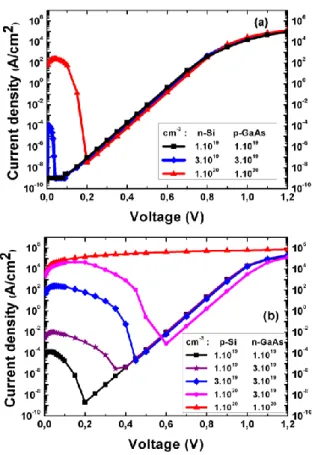
The targeted device is a junction that is suitable for low concentration applications. We already managed to grow a GaAs/GaAs tunnel junction with a sufficient Jpeak
of 20.8 A/cm2 [7] with a resistance of 1.7 mΩ.cm2.
Assuming that our typical JSC at one sun is of 20 mA.cm-2
and that we will work below 20 suns, we aim at a Jpeak of
400 mA.cm-2 at least with a resistance of 1.10-3 Ω.cm2 or
lower. Our objective is to see if the heterojunction between the III-V and the Si could play the role of a tunnel junction interconnecting the two subcells.
TCAD simulation have been performed considering only the non-local band-to-band mechanism with electrons and hole effective masses of me=0.328 and
mh=0.549 for Si and me=0.067 and mh=0.642 for GaAs.
We assume there are no traps at the interface that could further enhance Jpeak thanks to trap-assisted tunnelling
[8]. Also note that we inserted an additional series resistance Rs of 5.10-7ohm.cm2 to account for contact
resistances in the simulated tunnel junction device. Figure 1 shows the simulated J-V curves of (a) n-Si/p-GaAs (b) p-Si/n-n-Si/p-GaAs junctions, for different doping levels combinations. The n-type Si on p-type GaAs case is less favourable than the other device. We see that for doping levels of 1.1019 cm-3 there is no tunnelling
properties (black squares). For higher levels (3.1019 cm-3
on each side, blue diamonds), there is a tunnelling property but the peak current is below 1 mA.cm-3, which
is lower than our typical JSC at one sun (20 mA.cm-2). At
very high doping levels (1.1020 cm-3), a peak current at
around 200 A.cm-2 should be observed, which would be
enough for our targeted device. On the other hand, on Figure 1.b) simulations show better tunnelling properties for p-Si/n-GaAs, even at lower doping levels (1.1019 cm -3) and can reach a very high J
For doping level of 1.1020cm-3 in both p-Si and n-GaAs,
the typical negative slope of a tunnel junction cannot be seen, because the resistance of the device is so low that we are limited by the contact resistance Rs set at 5.10-7
Ω.cm2.
In this paper, we chose to grow both polarities, first of all to prove the feasibility of growing both p++ and n++
doped silicon by low temperature PECVD on GaAs, but also to compare the obtained devices with the simulation and to choose the best device to interconnect the subcells of our AlGaAs/Si(Ge) tandem cell.
3. EXPERIMENTAL METHODS
In order to grow the targeted devices, highly doped GaAs films have been deposited by MOVPE. Then, doped Si films have been epitaxially grown by low temperature (LT) PECVD on those GaAs films. For each film, we tried to reach the highest doping levels with the better crystalline quality.
3.1 MOVPE growth of GaAs
The III-V part of the tunnel junction has been grown by metalorganic vapour phase epitaxy (MOVPE) in a horizontal Aixtron 200 reactor available in the III-Vlab, on doped (100) GaAs wafers. The precursors used are TMGa and AsH3, while SiH4 and CBr4 were added for
the n-type and p-type doping respectively. Calibrations of the GaAs doped layers were made, using an Electrochemical Capacitance-Votage (ECV) to determine the doping level. The highest doping levels we could reach so far were 2.1019 cm-3 for the n-doped GaAs:Si,
and 1.1020 cm-3 for the p-doped GaAs:C.
3.2 Low-temperature PECVD growth of doped Si One of the critical parts of the targeted heterostructure is the growth of doped crystalline silicon on GaAs. The doped Si films were deposited in a multi-plasma chamber PECVD reactor operated a frequency of 13.56 MHz [9]. The depositions were performed at very low temperature (below 200°C) using silane (SiH4) and hydrogen (H2) gas
mixtures for the crystalline silicon films. The surface cleaning before the epitaxial growth is performed by an SiF4 plasma in the same reactor as the deposition [10].
All the films were characterized via spectroscopic ellipsometry using a phase modulated ellipsometer (UVISEL from HORIBA Jobin-Yvon) to determine their crystalline quality.
Previous works at the LPICM have shown the possibility of growing doped silicon on silicon (100) wafers [11]. The main challenge was to adapt the conditions to deposit these layers on doped GaAs grown by MOVPE. Other works in our laboratory emphasized that the GaAs surface cleaning is of high importance to allow the growth of intrinsic Si on GaAs [12]. By combining the previous knowledge and adapting the conditions to the epitaxial GaAs, we managed to grow both n-type and p-type silicon, with respective doping levels of 1.1020 cm-3 and 3.1019 cm-3. The details of these
PECVD growths are presented in the next part. 4 STRUCTURES AND DEVICES
4.1 n-Si on p-GaAs
n-type Si films were grown by PECVD at 175°C from the dissociation of a SiH4/H2 mixture combined with
phosphine (PH3). Figure 2 shows the imaginary parts of
the pseudo-dielectric function of n-doped silicon films grown on p-GaAs, together with the reference of the crystalline Si bulk. The two characteristic peaks of crystalline silicon can be seen at 3.4eV and 4.2eV, which confirms that we had an epitaxial growth. The decrease in the amplitude at high energy indicates a slight decrease in the film quality, due to the dopant incorporation. It has already been observed that the increase in doping level slightly decreases the film quality on n-type epitaxial Si films on (100) Si wafers. By Hall Effect measurements on the same film co-deposited on intrinsic GaAs wafer, we measure a doping level of 1.1020 cm-3.
Interestingly, we have been able to reach high doping levels (1.1020 cm-3) for both n-type Si and p-type GaAs.
Figure 2 : Ellispometry spectrum of n-Si deposited on
p-GaAs
Figure 1 : Simulated J-V curves of (a) n-Si/GaAs (b)
This polarity corresponds to the less favourable case for tunnelling (Figure 1.a)), but with such high doping levels, this structure should be able to behave as a tunnel junction according to simulation results reported previously.
4.2 p-Si on n-GaAs
The p-type Si films were grown at 150°C with trimethylboron (TMB) on a n-type GaAs grown by MOVPE (n++GaAs: 2.1019cm-3). Three different samples
(A, B and C) were grown with the same deposition conditions, but different thicknesses. Figure 3 shows the imaginary parts of the pseudo-dielectric function of p-doped silicon thin films grown on n-GaAs, together with the reference of the crystalline Si bulk.
Thus, we managed to grow p-Si with a doping level of about 3.1019 cm-3 on n-type GaAs (2.1019 cm-3). These
values are lower than those achieved for the opposite polarities, but should be high enough to enable tunnelling according simulations (see Figure 1.b)).
Table 1 summarizes the samples presented in this study.
Table 1 : List of samples presented in this study
Name Intern designation Si thickness Doping level in Si (cm-3) Support GaAs (cm-3) A-p 150619-5 60 nm p 3.1019 n 2.1019 B-p 150619-4 120 nm p 3.1019 n 2.1019 C-p 150619-6 180 nm p 3.1019 n 2.1019 n-Si 150619-2 180 nm n 1.1020 p 1.1020 4.3 Process flow
The structures were fabricated by standard technological steps in the III-V lab clean rooms: photolithography, metallisation by ion beam deposition, dry etching of the Si and wet etching of the GaAs. Several mesa structures with different sizes (from 100 µm to 500 µm) were etched, in order to check the reproducibility. The steps included a contact annealing at 400°C for 3 minutes.
Figure 4 shows the obtained structures. The J-V measurements were performed at room temperature at the GeePs, with four probes, including two back-probes electrically isolated, and two front probes. We used a keithley 2450 sourcemeter limited to 1A.
5 RESULTS AND DISCUSSIONS 5.1. n-Si/p-GaAs
According to the simulation, such high doping levels (1.1020 cm-3) in both p-type Si and n-type GaAs should
lead to a linear behaviour around 0V and a high peak current (Jpeak above 200 A.cm-2) for a few tens of mV.
Unexpectedly, we found a standard diode behaviour for the n-Si/p-GaAs sample, as reveals the J-V curve in Figure 5.
Several reasons may explain this unforeseen result, namely an underestimation of the doping level or an unintentional diffusion of silicon in the p-doped GaAs. Secondary ion mass spectrometry (SIMS) has been applied to investigate these points. The SIMS profile is presented in Figure 6. It reveals the presence of 2.1020
at/cm3 of P in the silicon layer, as well as 2.1020 at/cm3 of
C in the 30 nm layer of p++ GaAs. Those values are
consistent with the doping levels estimated by Hall Effect and ECV measurements. The silicon profile illustrated by the red squares and triangles curves shows a relatively sharp transition indicating that Si compensation effect can be neglected.
2
Figure 4 : Test structures of the heterojunctions
Figure 3 : Ellispometry spectra of p-Si deposited on
n-GaAs
Figure 5 : J-V curve n-Si/p-GaAs (reverse bias)
If the concentration of carbon in GaAs is indeed consistent with a doping level as high as 1.1020cm-3, we
can wonder if the exposition of the GaAs surface to the plasmas in the PECVD chambers could have affected the dopants. Literature reports effect of a H2 plasma on
p-doped GaAs [13]. The diffusion of hydrogen in the layer can lead to the formation of C-H complexes that neutralise the C dopants. Further investigations need to be performed in order to verify the hydrogen passivation of dopants in p-GaAs. Electrochemical Capacitance-Voltage (ECV) measurements on the final structure will soon be done to measure the active doping level in the GaAs after the step of Si deposition which includes an exposition to an H2 plasma. If this hypothesis is
confirmed, hydrogen exodiffusion experiments would be performed to reactivate the dopants.
5.2. p-Si/n-GaAs
Figure 7 shows the J-V characteristics of n++-GaAs/p+-Si of 3 samples grown with different Si thicknesses, measured at room temperature. The measurements were performed from -1V to +1V. A nearly linear behaviour was observed for each measurement until reaching saturation at 1A. The resistances were estimated to be 3.10-5 Ω.cm2, 3.10-4
Ω.cm2 and 5.10-4 Ω.cm2 for the A-p, C-p and B-p
samples, respectively. The J-V curves of the three samples showed a very low resistances (<10-3 Ω.cm2).
Linear characteristics have been observed up to current densities as high as 10.000 A.cm-2. We could not reach
higher currents because of the limitation of the measurement setup. With such low resistances, the voltage drop induced by the junction at our maximum working current density (400 mA.cm-2 at 20 suns) is
below 0.2 mV.
Nevertheless, we were not able to measure the typical negative slope of a tunnel junction. Metal contact resistance seems to be the limiting factor which restricts the tunnel current. Figure 8 shows the measured J-V curve (blue triangles) compared to the simulated ones with different doping levels. The red curve (sauqres) is simulated with a contact resistance of 3.10-5 Ω.cm2,
instead of the former value of 5.10-7 Ω.cm2. It is worth
noticing that in that case, when the contact resistance is close to the device resistance, the metallization-induced series resistance will be limiting the current and we will not observe the negative slope. TLM measurements are being currently performed in order to have a better insight on our contact resistance so as to implement it in the model.
Furthermore, the red curve in Figure 8 (squares) seems to fit with our experimental measurement, but corresponds to higher doping levels than in our samples. The high current density observed cannot be only explained by the probability of carrier tunnelling linked to the doping levels. There should be other mechanisms that could enhance the carrier tunnelling, such as TAT (trap-assisted tunnelling). Literature reports the strong impact of defects on tunnelling properties [8], [13], which could explain such low resistance and high current in our device. Other characterisations are ongoing to provide evidences of this contribution, e.g. Raman spectroscopy, studies after annealing and low-temperature J-V measurements. These experiments would enable to refine the model by adding a contribution of the traps in the simulations to have more realistic simulations.
In further studies, it will be important to have a good trade-off between the doping level (impacting the epi-Si crystal quality) and the junction performances (Jpeak >
400 mA.cm-2, R
peak < 1 mΩ.cm2): indeed for the final
targeted device (epi-Si(Ge) on III-V tandem cell), we need to keep a high crystal quality for the bottom Si(Ge) subcell.
CONCLUSION
In this paper we demonstrated the possibility of growing highly doped Si films by low temperature PECVD on GaAs despite the 4% lattice mismatch. First, we reported a n-Si/p-GaAs grown with high doping levels (1.1020 cm-3/1.1020 cm-3), with a standard diode
behaviour; contrary to what we were expected, there was no tunnelling effect. This might be due to a neutralization of p dopants in GaAs induced by the hydrogen plasma in the PECVD chamber. We also reported p-Si/n-GaAs junctions with very low resistance (below 5.10-4 Ω.cm2).
This exceeds by far our requirement for the interconnection between the two subcells of the targeted tandem solar cell. This junction seems to be suitable for integration in our Si/III-V tandem cell. Studies on the quality of the crystalline silicon are being currently led in order to understand the role of the defects in the tunnelling properties and to validate the compatibility of this junction with the further growth of the c-Si subcell.
Figure 8 : J-V Characteristics of p-Si/n-GaAs junction
compared to simulation. The red curve (squares) is simulated for Rs = 3.10-5 Ω.cm2
ACKNOWLEDGEMENT
This work was funded by the French National Research Agency within the IMPETUS project N°ANR-13-PRGE-0009-03.
[1] J. P. Connolly, D. Mencaraglia, C. Renard, et D. Bouchier, « Designing III–V multijunction solar cells on silicon », Prog. Photovolt. Res. Appl., janv. 2014.
[2] R. Lachaume, R. Cariou, J. Decobert, J. Alvarez, M. Foldyna, G. Hamon, P. Roca i Cabarrocas, et J.-P. Kleider, « Performance analysis of AlxGa1-xAs/epi-Si(Ge) tandem solar cells: a simulation study », E-MRS proceeding, To be published. [3] M. Hermle, G. Létay, S. P. Philipps, et A. W. Bett,
« Numerical simulation of tunnel diodes for multi-junction solar cells », Prog. Photovolt. Res. Appl., vol. 16, no 5, p. 409–418, 2008.
[4] J. F. Wheeldon, C. E. Valdivia, A. W. Walker, G. Kolhatkar, A. Jaouad, A. Turala, B. Riel, D. Masson, N. Puetz, S. Fafard, R. Arès, V. Aimez, T. J. Hall, et K. Hinzer, « Performance comparison of AlGaAs, GaAs and InGaP tunnel junctions for concentrated multijunction solar cells », Prog.
Photovolt. Res. Appl., vol. 19, no 4, p. 442–452,
2011.
[5] J. Yang, J. Goguen, et R. Kleiman, « Silicon Solar Cell With Integrated Tunnel Junction for Multijunction Photovoltaic Applications », IEEE
Electron Device Lett., vol. 33, no 12, p. 1732 ‑1734,
déc. 2012.
[6] J. Liang, L. Chai, S. Nishida, M. Morimoto, et N. Shigekawa, « Investigation on the interface resistance of Si/GaAs heterojunctions fabricated by surface-activated bonding », Jpn. J. Appl. Phys., vol. 54, no 3, p. 030211, mars 2015.
[7] R. Cariou, « Epitaxial growth of Si(Ge) materials on Si and GaAs by low temperature PECVD: towards tandem devices », phdthesis, Ecole Polytechnique, 2014.
[8] M. Baudrit et C. Algora, « Tunnel Diode Modeling, Including Nonlocal Trap-Assisted Tunneling: A Focus on III-V Multijunction Solar Cell Simulation », IEEE Trans. Electron Devices, vol. 57, no 10, p. 2564‑2571, oct. 2010.
[9] P. Roca i Cabarrocas, « A fully automated hot-wall multiplasma-monochamber reactor for thin film deposition », J. Vac. Sci. Technol. Vac. Surf. Films, vol. 9, no 4, p. 2331, juill. 1991.
[10] D. M. M. Moreno, « A comparative study of wet and dry texturing processes of c-Si wafers for the fabrication of solar cells », Sol. Energy, vol. 101, p. 182, 2014.
[11] J. Damon-Lacoste, M. Labrune, S. Granata, D. Daineka, et P. Roca i Cabarrocas, « Crystalline silicon solar cells with doped epitaxial silicon films obtained at low-temperature by PECVD », 2010, p. 001352‑001357.
[12] R. Cariou, J.-L. Maurice, J. Decobert, et P. Roca i Cabarrocas, « Direct epitaxial growth of silicon on GaAs by low temperature epitaxy », 2014, p. 2789‑2791.
[13] R. Rahbi, B. Pajot, J. Chevallier, A. Marbeuf, R. C. Logan, et M. Gavand, « Hydrogen diffusion and acceptor passivation in p-type GaAs », J. Appl.