Carbon Nanotube CMOS Analog Circuitry
by
Rebecca Ho
B.S., The University of Texas at Austin (2017)
Submitted to the Department of Electrical Engineering and Computer Science in partial fulfillment of the requirements for the degree of
Master of Science in Electrical Engineering and Computer Science at the
MASSACHUSETTS INSTITUTE OF TECHNOLOGY
June 2019
Massachusetts Institute of Technology 2019. All rights reserved
Signature redacted
Author...
Department of Electrical Engineering and Computer Science May 23, 2019
Signature
Certified by...
redacted
Max M. Shulaker
Emmanuel E. Landsman (1958) Career Development Assistant Professor of Electrical
Engineering and Computer Science
Thesis Supervisor
Accepted by...
MASSACHUSETTS INSTITUTE OF TECHNOLOGYJUN 13 2019
LIBRARIES
ARCHIV
Signature redacted
Leslie A. Kolodziejski
Professor of Electrical Engineering and Computer Science
Chair, Department Committee on Graduate Students
Carbon Nanotube CMOS Analog Circuitry
byRebecca Ho
Submitted to the Department of Electrical Engineering and Computer Science on May 23, 2019, in partial fulfillment of the
requirements for the degree of
Master of Science in Electrical Engineering and Computer Science
Abstract
Carbon nanotube (CNT) field-effect transistors (CNFETs) promise significant energy efficiency benefits versus today's silicon-based FETs. Yet despite this promise, complementary (CMOS) CNFET analog circuitry has never been experimentally demonstrated. This work presents the first reported demonstration of
CNFET CMOS analog circuits. For characterization, we fabricate analog building-block circuits such as
multiple instances of two-stage op-amps. These CNFET CMOS op-amps achieve gain >700, operate at a scaled sub-500 mV supply voltage, achieve high linearity, and are robust over time. Additionally, we demonstrate a front-end analog sub-system that integrates a CNFET-based breath sensor with an analog sensor interface circuit (transimpedance amplifier followed by a voltage follower to convert resistance change of the chemoresistive CNFET sensor into a buffered output voltage).
However, further progress in large-scale CNFET analog circuits is difficult to realize due to the inherent presence of metallic-CNTs (m-CNTs), which create an electrical short between the source and drain of a transistor and can result in excessive leakage current and severe degradation to analog circuit performance. Self-Healing Analog with RRAM and CNFETs (SHARC) is a novel circuit technique that leverages the programmability of resistive random-access memory (RRAM) to overcome the presence of m-CNTs for analog circuits. Here, we experimentally validate SHARC for multiple analog and mixed-signal circuit topologies. Using SHARC, we experimentally demonstrate the first mixed-signal and complex analog circuits fabricated with CNFETs.
Thesis Supervisor: Max Shulaker
Title: Emmanuel E. Landsman (1958) Career Development Assistant Professor of Electrical Engineering and
Acknowledgments
I would like to thank my thesis advisor Professor Max Shulaker for his mentorship, guidance, and the
countless hours that he has put into building his lab and supporting me in my research. His passion for this
field has served as constant motivation for me to work harder, and his enthusiasm for and patience in teaching has helped shape me into the researcher that I am today. It has been a privilege to have him as my advisor for
these past two years, and I look forward pursuing my PhD under his mentorship.
I would also like to thank Professor Harry Lee, who has taught me almost everything I know about analog
circuits and has provided me with invaluable guidance and insight in analog circuit design.
I am grateful to all of the members of NOVELS, who serve as my office mates, 24-hour user buddies,
mentors, and friends. I would particularly like to thank Dr. Gage Hills, who has taught me a great deal about
circuit simulation and design and is always willing to discuss The Bachelor. My research would not have
been possible without his work and guidance.
I am also grateful to Dr. Samuel Fuller, Denis Murphy, Andrew Olney, and Susan Feindt of ADI for their
advice in my graduate studies.
I would like to acknowledge all staff members and students of the Microsystems Technology Laboratories
(MTL), where I performed the majority of my research. In particular, I would like to thank Josh Perozek, Christian Lau, Pritpal Kanhaiya, Tathagata Srimani, and Dennis Ward for helping me with fabrication processes and keeping me company in the lab.
I would also like to thank Dr. Maryam Khodadoust for her support and insightful discussions, which have
helped me grow as a person outside of my research.
I am grateful to the National Science Foundation (NSF), which has provided me with financial support
through their Graduate Research Fellowships Program (GRFP).
I would like to thank my brother Garrison Ho, who is constantly impressing me with the risks he takes and
how hard he works. Lastly, I will always be grateful to my parents Julianne Trenary and Horace Ho for dedicating their lives to raising me, supporting me in my passions, and always welcoming me back home.
Table of Contents
A b stract ... 2
Acknowledgm ents ... 4
Table of Contents ... 5
L ist o f T ab le s ... 6
L ist o f Illu stratio n s ... 7
P erm issio n ... 8
Chapter 1: Introduction ... 9
1 .1 B ack g ro u n d ... 9
1 .2 C o n trib u tio n s ... 10
1 .3 O u tlin e ... I I Chapter 2: The First CN FET CM OS Analog Circuitry ... 12
2 .1 B ack g ro u n d ... 12
2.2 CNFET CM OS Process Flow ... 13
2.3 Experim ental Dem onstration of CN FET CM OS Analog Circuitry ... 14
2 .4 C o n clu sio n ... 18
Chapter 3: SHARC - Self Healing Analog with RRAM and CNFETs ... 19
3 .1 B ack g ro u n d ... 19
3.2 Principles of SHARC ... 20
3.3 SHARC Process Flow ... 22
3.4 Experim ental Dem onstration of SHARC ... 23
3 .5 C o n clu sio n ... 2 6 Chapter 4: Concluding Rem arks ... 27
List of Tables
List of Illustrations
Figure 1.1 Schem atic of a C N FET ... 10
Figure 2.1 Intrinsic gain benefits of CNFETs...13
Figure 2.2 CNFET CMOS process flow...13
Figure 2.3 ID-VDS curves for NMOS and PMOS CNFETs ... 14
Figure 2.4 Two-stage CNFET op-amp...15
Figure 2.5 CNFET analog sub-system...16
Figure 2.6 CNFET analog sub-system with sensor...17
Figure 3.1 Effects of a single m-CNT...19
Figure 3.2 Principles of SHARC...21
Figure 3.3 SHARC fabrication process flow...23
Figure 3.4 2-stage op-amp with SHARC...24
Figure 3.5 4-bit capacitive DAC with SHARC...25
Figure 3.6 4-bit SAR ADC with SHARC... 25
Permission
Part of this thesis has been reproduced with permission from R.Ho et al.:
1. Ho, Rebecca, Christian Lau, Gage Hills, and Max Shulaker. 2019. "Carbon Nanotube CMOS
Analog Circuitry." IEEE Transactions on Nanotechnology, 1-1.
https://doi.org/1 0.11 09/TNANO.2019.2902739.
2. Amer, Aya G., Rebecca Ho, Gage Hills, Anantha P. Chandrakasan, and Max M. Shulaker. 2019.
"29.8 SHARC: Self-Healing Analog with RRAM and CNFETs." In 2019 IEEE International
Chapter 1: Introduction
1.1 Background
While physical and equivalent scaling of silicon complementary metal-oxide semiconductor (CMOS)
technology has been a major driving force for improving computing energy efficiency for decades, continued
scaling is yielding diminishing returns. Unfortunately, progress in computing is halting at the exact moment
generation applications are demanding the largest gains in energy-efficiency. To enable these
next-generation applications, isolated advances (whether it be continued scaling, materials improvements, circuit
and system design, or software optimizations) alone are insufficient. Thus, coordinated advances across the
entire system stack - from materials to circuits to systems - are required. In this thesis, I explore both new nanomaterials, new circuit topologies designed around these new nanomaterials, and new system integrations
leveraging the unique properties of new nanodevices, in order to demonstrate future next-generation
electronic systems.
To begin realizing such new electronic systems, we initially focus on an emerging nanotechnology which are
the backbone of beyond-silicon electronic systems. Emerging one-dimensional (ID) and two-dimensional
(2D) semiconductors are exciting emerging nanomaterials, promising improved carrier transport and
electrostatic control versus bulk semiconductor materials (such as silicon). Single-walled carbon nanotubes
(SWCNTs, or CNTs), are one such promising 1 D nanomaterial with excellent electrical, thermal and physical
properties [Riichiro 1998; Wei 2009]. CNTs are nanocylinders made of a single atomically-thin sheet of
carbon atoms with a diameter of ~1 nm. Carbon nanotube field-effect transistors, CNFETs, are formed by
multiple CNTs in parallel forming the channel whose conductance is modulated by a metal gate. Figure 1.1
shows the schematic of a single CNT and a CNFET. Gate and source/ drain contacts are defined by traditional
lithography. Owing to their ultra-thin body thickness (~A nm diameter of the CNT), CNFETs exhibit excellent
electrostatic control and simultaneously high carrier transport [Hills 2015]. Due to these benefits, CNFETs
are projected to achieve an order of magnitude benefit in energy-delay product (EDP) compared to silicon
CMOS for digital VLSI circuits [Chang 2012; Wei 2009; Tulevski 2014]. Importantly, CNFETs can be
fabricated at low processing temperatures (<4000)a [Shulaker 2013a; Shulaker 2017; Patil 2009], and therefore naturally enable monolithic three-dimensional (3D) integration (whereby layers of circuits are
fabricated sequentially and directly vertically overlapping one-another, all over the same starting substrate.
Such monolithic 3D integration enables new paradigms in designing heterogeneous nanosystems [Shulaker
2017], allowing fine-grained integration of sensing, logic and memory at the nanoscale.
CNT Diameter
~1
nm
Figure 1.1: Schematic of carbon nanotube field-effect transistor (CNFET) with multiple parallel CNTs (nanocylinders made with atomically thin sheet of carbon atoms with diameter ~ I nm) bridging the source to drain
contact. Conductance of the CNTs are modulated by the gate to turn the transistor on or off.
Moreover, CNFETs are a rapidly maturing nanotechnology which has progressed substantially over
the past decade. CNFETs are unique among emerging nanotechnologies, as complete CNFET digital systems
[Shulaker 2013a; Shulaker 2014], highly-scaled CNFETs with sub-10 nm channel lengths [Franklin 2012], and complementary p- and n-type CNFETs operating at scaled supply voltages of <400 mV [Wei 2013] have
all been experimentally shown. However, prior to the work presented in this thesis, there has been no reported
demonstration of CNFET CMOS-based analog or mixed-signal circuits.
1.2 Contributions
In this thesis, I focus on utilizing the unique properties of CNTs to realize the first analog and mixed-signal
a While CNTs are synthesized at high temperature (>800 *C), they can be transferred to arbitrary substrates through either layer transfers or by solution-based processing at room temperature. This decouples the high-temperature processing of the CNTs from the monolithic 3D IC.
circuits fabricated with a CNFET CMOS technology. Specifically, this work shows the following:
1) By leveraging our CNFET CMOS process (which results in robust and well-matched NMOS and PMOS
CNFETs), we realize the first CNFET CMOS-based analog circuits. We demonstrate multiple instances of a 2-stage op-amp and a front-end analog sub-system that integrates a CNFET-based breath sensor with an analog sensor interface circuit (transimpedance amplifier followed by a voltage follower to convert resistance change of the chemoresistive CNFET sensor into a buffered output voltage). These experimental demonstrations are the first reports of CNFET CMOS analog functionality that is essential for a future
CNFET CMOS technology.
2) We combine the programmability of non-volatile resistive-RAM (RRAM) with CNFET-based analog circuits to experimentally demonstrate a "self-healing" circuit technique (SHARC: self-healing analog with
RRAM and CNFETs) that is robust to the major inherent imperfection of m-CNTs. This is the first
demonstration of CNFET-based mixed-signal circuits (4b-DAC and SAR ADC) and is the largest and most
complex CNFET CMOS yet demonstrated.
1.3 Outline
Chapter 2 presents the first reported experimental demonstration of CNT CMOS analog circuits, culminating
in a complete front-end analog sub-system. Chapter 3 demonstrates SHARC, a new circuit technique which
overcomes the presence of m-CNTs to enable large-scale CNFET-based analog and mixed-signal circuits.
Chapter 4 concludes this thesis.
Chapter 2: The First CNFET CMOS Analog Circuitry
2.1 Background
Carbon nanotubes (CNTs) are an emerging nanotechnology for next-generation electronics [Hills 2018;
Shulaker 2013a]. CNTs can be used to form CNT field-effect transistors (CNFETs), which owing to their
nanometer thin body (~1 nm CNT diameter) exhibit excellent electrostatic control and simultaneously high
carrier transport [Appenzeller 2008; Franklin 2012; Tulevski 2014]. Due to these properties, digital circuits
fabricated with CNFETs promise a 1Ox improvement in energy-delay product (EDP: a metric of energy
efficiency), versus silicon FETs [Hills 2018].
Despite these advantages, there remain major challenges towards realizing a future CNFET technology.
While a full complementary (CMOS) CNFET technology is required to realize the above energy-efficiency
benefits [Weste 2010], all complete digital CNFET systems have been fabricated from PMOS-only CNFETs
[Shulaker 2013a; Shulaker 2013b; Shulaker 2014; Shulaker 2017], and all reported CNFET CMOS
demonstrations have been limited to only individual devices, small-scale circuits, or digital logic [Lau 2018;
Shahrjerdi 2013; Yang 2017; Suriyasena Liyanage 2014; Zhang 2011; Ha 2015]. Importantly, due to the lack
of a robust CNFET CMOS process, there has been no reported demonstration of CNFET CMOS analog
circuitry (while the vast majority of circuitry in a system today is digital logic, analog circuits are still
essential for applications ranging from sense amplifiers for memory arrays to high speed input/output links
[Hodges 2004]). Moreover, similar to benefits for digital logic, CNFET CMOS promise analog circuit
performance benefits, providing additional motivation to realize CNFET CMOS for analog circuitry (Fig.
2.1).
First, I summarize our CNFET CMOS process flow (Chapter 2.2), followed by illustrating how we leverage
120 100 80 0) 60 40- 20-0 e
Figure 2.1: Intrinsic gain (gmro) [Razavi 2017] benefits of CNFETs. The intrinsic gain is extracted from circuit simulations (Cadence Spectre®) using commercial process design kits (PDKs) for silicon CMOS and using an experimentally calibrated compact model for CNFETs
(calibrated using CNFETs with sub-10 nm channel length) [Lee 2015].
2.2 CNFET CMOS Process Flow
Fig. 2.2 shows our CNFET CMOS fabrication flow [Lau 2018]. The CNFETs are fabricated with a back-gate
device structure with a metal gate (Pt) and high-k gate dielectric (20 nm HfO2deposited through atomic layer
1. Deposit Pt gate
4. Deposit PMOS S/D (Pt)
5. Deposit SiO2Passivation
2. Deposit ALD Hf02gate dielectic
3. Deposit and pattern CNTs
6. Deposit NMOS S/D (Ti)
7. Deposit ALD HfO2for NMOS doping '
Figure 2.2: CNFET CMOS process flow. A back-gate geometry is used for both the PMOS and NMOS CNFETs. All low-temperature (<250 'C) processing is performed with solid-state and silicon CMOS compatible materials.
13
Intrinsic Gain Benefit of CNFETs
-U U
-deposition, ALD). Post gate-stack fabrication, the CNTs are deposited through a solution-based incubation
process [Nanolntegris]. This solution-based CNT deposition enables the entire CNFET fabrication process
to be low temperature (<250 C)b. To fabricate the PMOS and NMOS CNFETs, we leverage a dual doping strategy which uses both source and drain metal contact work function engineering as well as oxide-based
electrostatic doping. The source and drain are lithographically patterned (0.5 nm Ti / 45 nm Pt for PMOS, 75
nm Ti for NMOS), and the PMOS CNFETs are encapsulated with SiOx while the NMOS devices are
encapsulated with ALD-deposited HfOx (the stoichiometry of the SiOx and HfOx sets the threshold voltage
of the PMOS and NMOS, respectively). This CNFET CMOS process leverages only solid-state and silicon
CMOS compatible materials, and results in well-matched PMOS and NMOS CNFETs (Fig. 2.3).
4 PMOS ,o'
NMOS
3 ,0
-1
0
-1.5 -1 -0.5 0 0.5 1 1.5 VDSeM
Figure 2.3: Characteristics of PMOS and NMOS CNFETs with a channel length of-2.5 pm and width of-4 pm. ID-VDS
curves show well-matched CNFET CMOS (i.e., with similar on-current for both NMOS and PMOS). VGs range from 0 V to VDD (1.8 V) with an increment of 0.1 V (for NMOS, VGS from 0 to -VDD for PMOS). Inset shows an ID-VGS curve of a
PMOS CNFET with ION/IOFF > 8000.
2.3 Experimental Demonstration of CNFET CMOS Analog Circuitry
As an initial demonstration of CNFET-based analog circuits, we fabricate a fundamental analog
building-block: a two-stage op-amp [Razavi 2017]. Fig. 2.4a displays the circuit schematic of our two-stage op-amp,
while Fig 2.4b shows a scanning electron microscopy (SEM) image of a fabricated CNFET CMOS op-amp.
Fig. 2.4c displays a voltage transfer curve for a differential amplifier (the first stage of the op-amp shown in
b The high-temperature growth process of CNTs is decoupled from the wafer substrate by using a solution-based incubation process to deposit CNTs. Such low-temperature fabrication enables greater CNFET integration, as the CNFETs can be fabricated in the back-end-of-line (BEOL) directly over silicon CMOS substrates.
Fig. 2.4a). Measurements of multiple instances of a two-stage op-amp are overlaid in Fig. 2.4d, where the differential input voltage (AVi. = Vin' - Vin-) is swept from -1 to 1 V (with a supply voltage of 2 V). The
op-amp achieves a maximum gain >700 (Fig. 2.4e). Device mismatch is minimal, with the average offset voltage
(VOFFSET, defined as the differential input voltage that achieves maximum gain) being VOFFSET < 12 mV.
(a)
2___(b)(C)
M7 WS M .8
WS 4M I WL Wul0. Win8 WNS
V6
0
Wa2.4 Gad WE.4 - eI+I.
Wd
2r hu 800 0 600 a *F 400 200 A _ _ _ _ _ _ -1 0 1 -1 0 1AVIN IN+ IN-) ( AV IN IN+-VIN-) M
Figure 2.4: Experimental demonstration of a single-ended two-stage amp using CNFETs. a) The topology of the op-amp is a differential op-amplifier followed by a common-source 2nd stage. b) SEM of the fabricated op-amp. c) Measured
waveforms of a CNFET-based differential amplifier (first stage of the two-stage topology) and d) multiple (three) instances of a two-stage op-amp, where the output voltage is a function of AVin (Vin' -Vin-). The output swing is >90% of VDD and
average VOFFSET < 12 mV, indicating well-matched devices. e) Derivative of the transfer-curve for the two-stage op-amp,
showing gain >700.
Leveraging this building block, we demonstrate a CNFET-based analog sub-system: a front-end integrated
sensor and sensor interface circuit that converts the resistance change of a chemoresistive CNFET sensor into
a buffered output voltage. The sub-system consists of a transimpedance amplifier (TIA) to convert the input
current (a function of the chemoresistive CNFET sensor) to a voltage, cascaded to a voltage buffer. To
characterize the sub-system, we initially fabricate the circuit shown in Fig. 2.5a. The CNFET chemoresistive
gas sensor is replaced with an externally controlled current source (IN) to remove any variability introduced
by the sensor itself. An SEM (false-colored for clarity) of the fabricated circuit is shown in Fig. 2.5b. To
characterize the circuit, we sweep a DC current at the input of the system and measure the corresponding
voltage output from the voltage buffer. Fig. 2.5c shows the measured output (with a 2 V supply voltage); as
15
Gain
expected, the output voltage changes linearly with the input current over the entire input range (10 pA to 50
ptA, designed the match the chemoresistive sensor). To quantify the linearity of the response, we calculate
the coefficient of determination, R2, for the measured response to a best-fit linear line [Rao 2001]. The
average R2 across the entire input range is 0.999, illustrating high linearity (e.g., the measured response
closely follows a linear relationship to input current). Moreover, Fig. 2.5d shows 100 repeated measured
waveforms overlaid on top of one-another, illustrating robust operation with minimal drift.
(a)
(c) 0.6 VDD = 2V 0.5 0.4 0.3 R2=0.998 0.3 R2=O.998 0.2 VD Z 10 20 30 40 50 /IN (PA) (e)0.35 VDD = 480mV 0.3 r 6 0.251 S0.2j 0.15, R2=.997' 0.1 15 20 25 IN (P)(b)
OL(d)
o.6,7 VDD =2V 0.5 0.4' 0.3 R2=0.999 0.1~ 10 20 30 40 50 'IN (P) 0.35! 0 VDD = 480mV 0.3 0.251 ~h0.21 0.15 R2=0.998 0.1* 15 20 25 IN (PA)Figure 2.5: Characterization of analog sub-system, with the CNFET sensor replaced with an external current source. (a-b) Schematic and SEM. (c) Measured linear response of the sub-system, converting input current to output voltage. (d) 100 repeated measurement cycles, illustrating minimum drift. (e-f) Repeated measurements of (c-d), with supply voltage reduced
from 2 V to 480 mV. Functionality and linearity are not sacrificed even at scaled <500 mV supply voltages.
Additionally, we show the CNFET CMOS circuitry can operate at scaled supply voltages without degrading
key circuit performance metrics. Fig. 2.5(e-f) shows the response of the system with a scaled 480 mV supply
voltage. The measured response still exhibits high linearity (R2 value of 0.998 to a best-fit linear line), as
well as similarly minimal drift over 100 repeated measurements.
Fig. 2.6 shows the complete integrated sensor and sensor interface sub-system. As shown in the schematic in
Fig. 2.6a, an on-chip integrated CNFET chemoresistive gas sensor replaces the external DC current supply
at the input of the TIA. The CNFET chemoresistive gas sensor is fabricated using the same process flow shown in Fig. 2.2c, but all of the oxide covering the CNFET chemoresistive gas sensor is removed with a dilute HF wet etchd. Thus, the CNFET chemoresistive gas sensor is exposed to the environment, while all other CNFETs (e.g., the CNFETs comprising the amplifiers) are encapsulated with a dielectric and are thus protected from the ambient. An SEM of the fabricated sub-system is shown in Fig. 2.6b. To characterize the response of the sub-system, the sensor is kept in a controlled constant ambient (e.g., dry air), and the input voltage (VN, Fig. 2.6c-d) applied across the sensor is swept. Similar to the sub-system in Fig. 2.5 with a constant current source as the input, the measured output voltage (VOUT) of the sub-system exhibits high
(a)
R(b)
PMS CNFET senr Resbstorl (C) 1(d)
16 1.4 1.2 D ~1 0.8 R2=.999 R2=0.998 0.5 0.6 0.6 0.8 1 1.2 1.4 1.6 0.4 0.6 0.8 1 1.2 1.4 1.6 2-1.5 1-0.5 00 1 2 3 4 5 6 7 8 time (min)Figure 2.6: Characterization of analog sub-system, with an on-chip integrated CNFET chemoresistive breath sensor. (a-b) schematic and SEM. (c) Measured linear response of the sub-system, measured by keeping the sensor in N2 ambient air and
sweeping the input voltage, Vn+, applied across the sensor. The response is highly linear with a R2 value of 0.999. (d) 10,000 repeated measurement cycles, illustrating minimum drift. The first 2500 cycles are red, the next 2500 cycles are yellow, the next 2500 cycles and light blue, and the last 2500 cycles are dark blue. The spread in the measured outputs is not random noise, but rather minor slow drift of the circuit after constant measuring for 12 hours. Future work can improve
upon stability by optimizing the gate stack to minimize interface traps at the CNT-gate dielectric interface. (e) Measured response of the sub-system in response to alternative exposures to warm breath and N2. The oscillating response in the
circuit illustrates correct functionality of the integrated sensor/ sensor interface circuit.
The CNFET chemoresistive gas sensor is also functionalized with a polymer to increase its sensitivity to ambient conditions. There is rich literature describing the design and fabrication of CNFET gas sensors (Kong 2000; Liu 2015; Zhang 2006).
d The dilute HF wet etch has a high etch selectivity of SiOx over HfOx and does not etch or degrade the CNTs.
17
linearity (R2 value of 0.999 to a best-fit linear line). Moreover, Fig. 2.6d shows the circuit is robust and air-stable: 10,000 repeated DC measurements performed over 12 hours illustrate minimal drift.
To test the full integrated sensor and sensor interface circuity, we alternate between one-minute intervals of
breathing and blowing N2 gas directly over the sensor. The CNFET gas sensor reversibly responds to warm breath, resulting in the front-end sub-system voltage output toggling between ~0 V and ~2 V, illustrating correct functionality of the circuit with successful detection and response to breath.
2.4 Conclusion
We present the first demonstration of CNFET CMOS analog circuits by fabricating foundational building block op-amps up to an analog-based sensor interface circuit. As an experimental demonstration, we integrate the sensor interface circuit with an on-chip chemoresistive CNFET gas sensor, illustrating response and detection of breath. The CNFET CMOS analog circuits achieve high gain (>700) and linearity and operate at scaled sub-500 mV supply voltages (without sacrificing linearity). Thus, this experimental work is a key step towards demonstrating analog functionality that is essential for a future CNFET CMOS technology.
'I
Chapter 3: SHARC
-
Self Healing Analog with RRAM and CNFETs
3.1 Background
While CNFETs promise performance benefits for analog circuitry, CNTs suffer from a major inherent imperfection: every ensemble of CNTs contains some metallic-CNTs (m-CNTs), which cause an electrical short between the CNFET source and drain. This results in substantial leakage current and degradation in circuit performance (or even catastrophic circuit failure). Although techniques have been developed to further purify CNT solutions and enable the demonstration of digital CNFET circuits (digital circuits can still maintain correct functional operation even in the presence of a limited number of m-CNTs) [Zhang 2009],
ideal ID vs. VGs 0 - - S-CNT -0 -S 0 01 0 0.2 0.4 0.6 0.8 1 VGa (V)
DAC OP-AMP (Folded Cascode) with m-CNTs location VDD (2) (2) (2) (3a) (3a) (2)(2) (2) Vout Vb (4) (4) (3b) (3 (3b)
b)
150 5I 00 50 Cd)
0. 0. 0' 0. 0-0 0 0.2 0.4 0.6 0.8 1 VGS(M8-bit DA C transfer curve
8 6- 3 s 2,3a,4 4 - SW 2 0 50 100 150 200 250 D. (decimal value)
Figure 3.1: CNFET schematics and ID-VGS curves for a) a CNFET with all semiconducting-CNTs (s-CNTs) and b) a CNFET with a single m-CNT. Leakage current (defined as the current through the transistor when it is off) is higher in the presence of an m-CNT. c) Schematic of an 8-bit DAC designed with an op-amp. Transistors in the DAC are color-coded to match d) graph of the output voltage of the DAC with different placements of a single m-CNT in the CNFET channel. The compact model used for circuit simulations is calibrated to experimental data for the 10 nm technology
node (m-CNT off-state resistance is 25 KfI).
19 0 5
a)
15 Iz
aC)
1vs. V with m-CNT . S-CNTM-N -- Nm-CNTs present a major obstacle to realizing large-scale analog and mixed-signal circuits. The effects of a
single CNT on the performance of an 8-bit DAC are displayed in Fig. 3.1 for different locations of the
m-CNT within the circuit, illustrating that even a single m-m-CNT can cause catastrophic circuit failure for analog
circuits (e.g., the output of the DAC latches to either VDD of ground due to a single m-CNT placed within a
single CNFET in the circuit).
3.2 Principles of SHARC
Here, we present a new circuit design technique that overcomes the presence of m-CNTs in analog circuits.
By combining the programmability of non-volatile resistive-RAM (RRAM) with the ability to fabricate
monolithic 3D circuits with CNFETs, we demonstrate a circuit design technique whereby a circuit can
"self-heal" in the presence of m-CNTs.
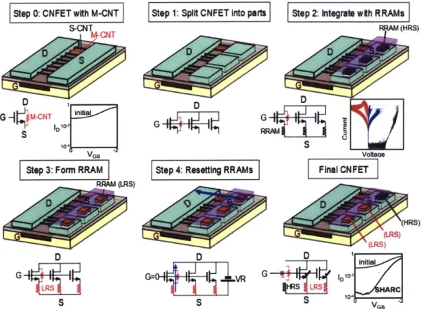
The process of SHARC is displayed in Fig. 3.2. First, CNFETs are fabricated, with each CNFET in the circuit
topology split into multiple minimum-width FETs (which we refer to as "sub-CNFETs"). An RRAM cell is
fabricated directly over (or under) the source or drain contact of each CNFET so that each CNFET is in series
with an RRAM cell. Critically, the RRAM fabrication directly over or under the sub-CNFET contact
minimizes the area penalty of SHARC and is directly enabled by the low-temperature fabrication of the CNFETs and RRAM (e.g., the high-temperature >1000 'C fabrication of silicon FETs would damage or
destroy any devices previously fabricated underneath the silicon FET on a wafer). Both RRAM and CNFETs
require <400 'C processing, and thus naturally enable such heterogeneous monolithic 3D integration. After fabricating the RRAM and CNFETs, the RRAM cells are then "formed" by applying a positive voltage across the RRAM electrodes, which sets the RRAM into a low-resistance state (LRS). The RRAM stack is designed so that its form voltage is higher than the operating voltage of the circuit, preventing any unwanted programming of the RRAM during circuit operation. Next, a voltage is applied across the source and drain of each CNFET, with the gates of the CNFETs biased so that each transistor is in its off-state (e.g., IVGSI <
IVTHI). Thus, if a CNFET contains only semiconducting CNTs (s-CNTs), it will not conduct current.
sufficient biasing and current, the RRAM in series with CNFETs containing m-CNTs are reset to their
high-resistance state (HRS). This effectively "self-heals" the circuit, by automatically programming the RRAM in
series with CNFETs containing m-CNTs in a high-resistance, effectively removing that CNFET from the
circuit. To ensure proper resetting of the RRAM, the reset current of the RRAM should be designed to be
less than the off-state leakage current through an m-CNT (<100 pA for a scaled technology node). The last
step in the SHARC process is to fabricate the final metal layers of the circuit. The final result is a CNFET
circuit where sub-CNFETs containing only s-CNTs are in series with RRAM in a LRS, while sub-CNFETs
containing any m-CNTs are in series with RRAM in a HRS. Post self-healing, CNFETs containing m-CNTs
experimentally exhibit ION/IOFF > 1000 and IOFF reduces >800x.
Stop 0: CNFET with M-CNT S-CNT GCCTC D S D S VGS Stop 3: Form RRAM
RRAM (LRS)
D
D
G
S
Step 1: SpIlt CNFET Into parts Step 2: Integrale wth RRAMs
D
G 4
Stop 4: Resatng RR AMs
(HRS) D D IFinal CNFET D 40 )(HRS) (LRS) (LRS) D D na
G=" 1
1171
Y101
71
G 1tR 104 :zC S S VGSFigure 3.2: Principles of SHARC. The initial and final ID-VGS curves when using SHARC are shown in step 0 and the final step. ION/IOFF of all sub-CNFETs combined is improved from -10 before SHARC to >1000 in the final step. Steps 1 through 4 illustrate how the RRAM is first formed to a low-resistance state (LRS) and then reset to a high-resistance state
(HRS) in the presence of an m-CNT. In the final step, an RRAM in a high-resistance state is shown in series with a sub-CNFET containing an m-CNT.
SHARC is a broad technique that can be applied to a wide range of analog circuit blocks and scales to
larger-scale circuits, since SHARC only has to be performed once for all CNFETs in parallel. Additional parameters
in the circuit design of SHARC, such as the minimum ratio between RRAM high- and low-resistance states
(in order to prevent drawing excessive current from the power supply) or RRAM cell placement (e.g., on the drain of input CNFETs instead of the source), must also be taken into consideration, and are analyzed in
detail in [Amer 2019].
The key benefits of SHARC are: (1) since the m-CNTs provide the current path for resetting the RRAM
during the self-healing process (e.g., RRAM programming), the self-healing process occurs automatically
(2) because of the low-temperature fabrication of both CNFETs and RRAM (<300 C), they can be fabricated
directly vertically overlapping one-another in a monolithic three-dimensional fashion, minimizing area
penalty associated with SHARC, and (3) RRAM is non-volatile, allowing the circuit to retains its healed
configuration (though due to their programmability, the RRAM can potentially be reprogrammed repeatedly
in the future).
3.3 SHARC Process Flow
The fabrication process flow for SHARC is displayed in Fig. 3.3. First, the bottom electrodes of the RRAM
are lithographically patterned and deposited (3 nm Ti/ 30 nm Pt), followed by deposition of the RRAM oxide (5 nm HfO2). Prior to the deposition of the RRAM top electrodes, a 2-minute oxygen plasma descum
is performed to remove any residue on the circuit's surface and prevent delamination of later metal layers.
A back-gate geometry is used for the CNFETs, allowing the top RRAM electrodes and gates of the
CNFETs (25 nm TiN/ 25 nm Pt) to be deposited simultaneously (this is not a requirement, but highlights how process complexity can be reduced through careful processing-circuit co-optimization). The RRAM
are then formed to their low-resistance state. The CNFETs are fabricated up to the source/drain layer by the same process described in Section 2.2, with slight modifications to the source/drain metal layer (1 nm Ti/
70 nm Pt for PMOS, 72 nm Ti! 3 nm Pt for NMOS). A sacrificial metal layer (0.5 nm Ti! 15 nm Al) is
deposited to perform the circuit self-healing step. The sacrificial metal layer is removed, and the CNFETs are passivated and doped as described in Section 2.2. In the final step of the process, the final metal routing
layer is lithographically defined and deposited.
RRAM electrode
RRAM oxide
RRAM electrode
+ CNFET
qates
RRAM form
CNFET gate oxide
CNT deposition
Via + CNFET
"self-healing"
Final metal
source/drain
routing layers
Figure 3.3: Fabrication process flow of SHARC.
3.4 Experimental Demonstration of SHARC
As an experimental demonstration of SHARC with analog and mixed-signal circuits, we use SHARC to
fabricate a stage op-amp, 4-bit digital-to-analog converter (DAC, SHARC implemented in the
two-stage op-amp and switches), and a 4-bit successive approximation register analog-to-digital converter (SAR
ADC, SHARC implemented in the strong-arm latch and switches). All demonstrations are implemented at
a relaxed 2 pm technology node due to the limitations of an academic fabrication facility (importantly, SHARC, the CNFET CMOS process, and all other aspects of this work can be scaled to arbitrary
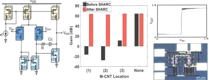
technology nodes). As an example of the impact of SHARC, Fig. 3.4 shows the effects of an m-CNT on a
two-stage op-amp. Without SHARC, a single m-CNT within the circuit can reduce gain by >100 dB
(making the amplifier an attenuator). However, with SHARC, the worst-case gain reduction is <3 dB. To
illustrate a functional circuit implementing SHARC (e.g., that the circuit still functions with the full
monolithic 3D process flow integrating RRAM and CNFETs), we fabricate this two-stage op-amp using
SHARC. The results are shown in Figure 3.4; gain is >800 and matches simulations performed with
experimentally calibrated CNFET and RRAM compact models. Fig. 3.5 displays the schematic and die
image of a 4b DAC. The measured transfer characteristics show monotonic behavior with non-linearity and
-n
gain error (due to large parasitic caps and routing resistance). Fig. 3.6 shows the SAR ADC schematic, its
die image and its transfer characteristics.
These circuits are the first demonstration of mixed-signal and complex analog CNFET circuits, and the
largest and most complex reported CNFET CMOS circuits to-date (see Table 3.1 for comparison to
previous works [Geier 2015; Han 2017; Tang 2018; Yang 2017; Zhang 2018]).
VDD (3 3) (3 vin. vin ref nr i+ 'rf 1) (1 Cc R (2 (2 2) V V .oVout. -C, 80 -- Before SHARC M ter SHAC 60 40 20 01 -20 -40 (1) (2) (3) M-CNT Location
Figure 3.4: Two-stage op-amp with SHARC. (left) Schematic. (middle) Gain (dB) of op-amp when an m-CNT is located in different locations of the op-amp (labeled in schematic) before and after SHARC. Before SHARC, gain can reduce by >100 dB, while after SHARC gain is reduced by a maximum of 3 dB. (right) Die photo and experimental measurement of op-amp
using SHARC, achieving gain >800.
Circuit CNFETs Reference per Circuit
4b-ADC 306 This Work
4-bit full adder 132
Inverter 2 Yang et al. SRAM Cell 6 Geier et al.
Inverter 2
Ring Oscillator 12 Han et al. Inverter 2 Tang et al. Inverter 2 Zhang et al.
Table 3.1: Comparison of this work to state-of-the-art CNFET CMOS demonstrations.
1.8
VDD=1-8
2 stage-opamp
X Vout
I8Cu ,,,,,, 2CU CU
10
= ref M ref = ref CK
D3 CLK D 1 CLK Do CLK Measured Ideal 2 4 6 8 10 12 14 Din sigma INL - .0_j21 z-J M 0 1 2 3 4 5 6 7 8 9 10 11 12 13 14 15 Digital Code sigma DNL r z 0 E 16 ' 1 2 3 4 5 6 7 8 9 10 11 12 13 14 15 Digital Code
Figure 3.5: 4-bit capacitive DAC with SHARC. (top) Schematic and die photo. (bottom) Measured characteristics show the monotonic behavior with offset (50mV) and non-linearity where the maximum GINL and ODNL is 0.8 LSB.
CLKb
VCM 8CU ,,,,, 12Cu J. CU
CU
Vref i ref = ref
3 i Bseates B BO CLK CLK CLK S Latch SAR Logic D3 D2 Di Do ,, . ~Ideal._~ . 10- Ideal 5. 1 Measured 0 0 0.2 0.4 0.6 0.8 1 1.2 1.4 1.6 1. Vin (Volt) z a 0.6-0.4 0.2 0 -0.2 .0.4-8 1 2 3 4 5 6 7 8 9 10 11 12 13 14 15 Dout
Figure 3.6: 4-Bit SAR ADC with SHARC. (top) Schematic and die photo. (bottom) Measured characteristics show the ADC behavior with offset (35mV), non-linearity and gain error whereas the DNL (-0.5 LSB->0.75 LSB).
25 .-S04AP MA 1.6 1.4 1.2 >1 0.8 0.6 0 a
3.5 Conclusion
We experimentally validate a new circuit design technique, SHARC, that overcomes the presence of
m-CNTs on analog circuits. This technique is enabled by the programmability of non-volatile RRAM, and it
utilizes the ability to fabricate monolithic 3D circuits with CNFETs. By placing RRAM in series with the
CNFETs, the circuit is able to automatically "self-heal" by resetting any RRAM in series with an m-CNT
to its high-resistance state. Using SHARC, we experimentally demonstrate the first mixed-signal and complex analog circuits with CNFETs. The implementation of SHARC at the CNFET-level gives it versatility; it can be combined with additional existing circuit techniques to further improve performance, such as technology node scaling to improve energy efficiency and existing circuit topologies to improve linearity. Thus, SHARC can be leveraged to realize large-scale, energy-efficient analog and mixed-signal
Chapter 4: Concluding Remarks
CNTs are an emerging nanotechnology that promise significant EDP benefits for digital VLSI design [Tulevski 2014; Wei 2009]. Yet despite this promise, no analog circuits have ever been demonstrated with
CNFET CMOS. By leveraging our CMOS CNFET fabrication process, we experimentally demonstrate the
first CNFET CMOS-based analog circuitry up to a complete analog-based sensor interface circuit.
Despite this progress, the unavoidable presence of metallic-CNTs (m-CNTs) prohibited the realization of large-scale and increasingly complex CNFET-based analog circuits. While new techniques have been
developed to enable the fabrication of CNFET digital logic even in the presence of m-CNTs, a single m-CNT
can cause catastrophic functional failure to analog circuits. Self-healing Analog with RRAM and CNFETs
(SHARC) is a new circuit design technique to overcome the presence of m-CNTs for analog circuits. SHARC
leverages heterogeneous monolithic 3D integration of CNFETs and RRAM to enable circuits to
automatically "self-heal" in the presence of m-CNTs, while still maintaining transistor matching and proper
operation within the circuit. With this technique, we experimentally demonstrate the first mixed-signal and
complex analog circuits with CNFETs.
This work illustrates the potential - and promise - of CNFETs for analog circuitry. By demonstrating the ability to realize these analog circuit building blocks, this work is the foundation for future efforts to realize
increasingly complex CNFET-based systems. For instance, by leveraging the low-temperature fabrication
process of CNFETs, novel systems and architectures - such as vertical layers of sensing, sensor interface circuitry, and computing logic - can be fabricated directly over one another in a monolithic 3D fashion. Such systems will be able to capture raw data from the outside world and compute on it - all within the same chip. As progress continues to be made in these underlying nanotechnologies, we aim to realize the promise and
benefits of these beyond-silicon technologies.
References
[Amer 2019] [Appenzeller 2008] [Chang 2012] [Dennard 1974] [Franklin 2012] [Geier 2015] [Han 2017] [Ha 2015]Amer, Aya G., Rebecca Ho, Gage Hills, Anantha P. Chandrakasan, and Max M.
Shulaker. 2019. "29.8 SHARC: Self-Healing Analog with RRAM and CNFETs." In
2019 IEEE International Solid-State Circuits Conference-(ISSCC), 470-72. IEEE.
Appenzeller, J. 2008. "Carbon Nanotubes for High-Performance
Electronics-Progress and Prospect." Proceedings of the IEEE 96 (2): 201-11.
Chang, L. IEDM short course. IEDM, 2012.
Dennard, Robert H., Fritz H. Gaensslen, V. Leo Rideout, Ernest Bassous, and Andre
R. LeBlanc. 1974. "Design of Ion-Implanted MOSFET's with Very Small Physical
Dimensions." IEEE Journal of Solid-State Circuits 9 (5): 256-68.
Franklin, Aaron D., Mathieu Luisier, Shu-Jen Han, George Tulevski, Chris M.
Breslin, Lynne Gignac, Mark S. Lundstrom, and Wilfried Haensch. 2012. "Sub-10
Nm Carbon Nanotube Transistor." Nano Letters 12 (2): 758-62.
Geier, Michael L., Julian J. McMorrow, Weichao Xu, Jian Zhu, Chris H. Kim, Tobin
J. Marks, and Mark C. Hersam. 2015. "Solution-Processed Carbon Nanotube
Thin-Film Complementary Static Random Access Memory." Nature Nanotechnology 10
(11): 944-48.
Han, Shu-Jen, Jianshi Tang, Bharat Kumar, Abram Falk, Damon Farmer, George
Tulevski, Keith Jenkins, et al. 2017. "High-Speed Logic Integrated Circuits with
Solution-Processed Self-Assembled Carbon Nanotubes." Nature Nanotechnology 12
(9): 861-65.
[Hills 2015] [Hills 2018] [Hodges 2004] [Zhang 2009] [Kong 2000] [Lau 2018]
Javey. 2015. "Highly Uniform and Stable N-Type Carbon Nanotube Transistors by Using Positively Charged Silicon Nitride Thin Films." Nano Letters 15 (1): 392-97
Hills, Gage, Jie Zhang, Max Marcel Shulaker, Hai Wei, Chi-Shuen Lee, Arjun Balasingam, H.-S Philip Wong, and Subhasish Mitra. 2015. "Rapid Co-Optimization of Processing and Circuit Design to Overcome Carbon Nanotube Variations." IEEE Transactions on Computer-Aided Design of Integrated Circuits and Systems 34 (7):
1082-95.
Hills, G., M. Garcia Bardon, G. Doornbos, D. Yakimets, P. Schuddinck, R. Baert, D. Jang, et al. 2018. "Understanding Energy Efficiency Benefits of Carbon Nanotube Field-Effect Transistors for Digital VLSI." IEEE Transactions on Nanotechnology,
1-1.
Hodges, David, Horace Jackson, and Resve Saleh. 2004. Analysis and Design of Digital Integrated Circuits. 3rd ed. New York, NY, USA: McGraw-Hill, Inc.
Jie Zhang, N.P. Patil, and S. Mitra. 2009. "Probabilistic Analysis and Design of Metallic-Carbon-Nanotube-Tolerant Digital Logic Circuits." IEEE Transactions on Computer-Aided Design of Integrated Circuits and Systems 28 (9): 1307-20.
Kong, Jing, Nathan R. Franklin, Chongwu Zhou, Michael G. Chapline, Shu Peng, Kyeongjae Cho, and Hongjie Dai. 2000. "Nanotube Molecular Wires as Chemical Sensors." Science 287 (5453): 622-25.
Lau, Christian, Tathagata Srimani, Mindy D. Bishop, Gage Hills, and Max M.
Shulaker. 2018. "Tunable N-Type Doping of Carbon Nanotubes Through Engineered
Atomic Layer Deposition HfOX Films." ACS Nano, October.
[Liu 2015] [Nanolntegris] [Patil 2009] [Rao 2001] [Riichiro 1998] [Sabry 2015] [Shahrjerdi 2013] [Shulaker 2017]
Liu, Sophie F., Lionel C. H. Moh, and Timothy M. Swager. 2015. "Single-Walled
Carbon Nanotube-Metalloporphyrin Chemiresistive Gas Sensor Arrays for Volatile
Organic Compounds." Chemistry ofMaterials 27 (10): 3560-63.
"Nanolntegris." http://nanointegris.com/.
Patil, N., A. Lin, E.R. Myers, Koungmin Ryu, A. Badmaev, Chongwu Zhou, H.-S.P.
Wong, and S. Mitra. 2009. "Wafer-Scale Growth and Transfer of Aligned
Single-Walled Carbon Nanotubes." IEEE Transactions on Nanotechnology 8 (4): 498-504.
C. Radhakrishna Rao. 2001. Linear Statistical Inference and Its Applications, 2nd
Edition. Second edition.
Saito Riichiro, G. Dresselhaus, and Mildred S. Dresselhaus. 1998. Physical
Properties Of Carbon Nanotubes.
Sabry, Mohamed M., Mingyu Gao, Gage Hills, Chi-Shuen Lee, Greg Pitner, Max M.
Shulaker, Tony F. Wu, Mehdi Asheghi, Jeff Bokor, and Franz Franchetti. 2015.
"Energy-Efficient Abundant-Data Computing: The N3XT 1,000 X." Computer 48 (12): 24-33.
Shahrjerdi, Davood, Aaron D. Franklin, Satoshi Oida, John A. Ott, George S.
Tulevski, and Wilfried Haensch. 2013. "High-Performance Air-Stable N-Type
Carbon Nanotube Transistors with Erbium Contacts." ACS Nano 7 (9): 8303-8.
Shulaker, Max M., Gage Hills, Rebecca S. Park, Roger T. Howe, Krishna Saraswat,
H.-S. Philip Wong, and Subhasish Mitra. 2017. "Three-Dimensional Integration of
Nanotechnologies for Computing and Data Storage on a Single Chip." Nature 547
[Shulaker 2013a] [Shulaker 2014] [Shulaker 2013b] [Suriyasena Liyanage [Tang 2018] [Tulevski 2014] [Wei 2013]
Shulaker, Max M., Gage Hills, Nishant Patil, Hai Wei, Hong-Yu Chen, H.-S. Philip
Wong, and Subhasish Mitra. 2013. "Carbon Nanotube Comp1ter." Aature 501
(7468): 526-30.
Shulaker, M. M., J. Van Rethy, G. Hills, H. Wei, H. Chen, G. Gielen, H.- P. Wong,
and S. Mitra. 2014. "Sensor-to-Digital Interface Built Entirely With Carbon
Nanotube FETs." IEEE Journal ofSolid-State Circuits 49 (1): 190-201.
Shulaker, M., J. Van Rethy, G. Hills, H. Chen, G. Gielen, H.- P. Wong, and S. Mitra.
2013. "Experimental Demonstration of a Fully Digital Capacitive Sensor Interface
Built Entirely Using Carbon-Nanotube FETs." In 2013 IEEE International
Solid-State Circuits Conference Digest of Technical Papers, 112-13.
2014] Suriyasena Liyanage, Luckshitha, Xiaoqing Xu, Greg Pitner, Zhenan Bao,
and H.-S. Philip Wong. 2014. "VLSI-Compatible Carbon Nanotube Doping
Technique with Low Work-Function Metal Oxides." Nano Letters 14 (4): 1884-90.
Tang, Jianshi, Qing Cao, George Tulevski, Keith A. Jenkins, Luca Nela, Damon B.
Farmer, and Shu-Jen Han. 2018. "Flexible CMOS Integrated Circuits Based on
Carbon Nanotubes with Sub-10 Ns Stage Delays." Nature Electronics 1 (3): 191-96.
Tulevski, George S., Aaron D. Franklin, David Frank, Jose M. Lobez, Qing Cao, Hongsik Park, Ali Afzali, Shu-Jen Han, James B. Hannon, and Wilfried Haensch.
2014. "Toward High-Performance Digital Logic Technology with Carbon
Nanotubes." ACS Nano 8 (9): 8730-45.
Wei, Hai, Max Shulaker, H.-S. Philip Wong, and Subhasish Mitra. 2013.
"Monolithic Three-Dimensional Integration of Carbon Nanotube FET
[Wei 2009] [Weste 2010] [Yang 2017] [Zhang 2018] [Zhang 2011] [Zhang 2006]
Complementary Logic Circuits." In 2013 IEEE International Electron Devices
Meeting, 19-7. IEEE.
Wei, Lan, David J. Frank, Leland Chang, and H.-S. Philip Wong. 2009. "A
Non-Iterative Compact Model for Carbon Nanotube FETs Incorporating Source
Exhaustion Effects." In 2009 IEEE International Electron Devices Meeting (IEDM), 1-4. IEEE.
Weste, Neil, and David Harris. 2010. CMOS VLSI Design: A Circuits and Systems
Perspective. 4th ed. USA: Addison-Wesley Publishing Company.
Yang, Yingjun, Li Ding, Jie Han, Zhiyong Zhang, and Lian-Mao Peng. 2017.
"High-Performance Complementary Transistors and Medium-Scale Integrated Circuits
Based on Carbon Nanotube Thin Films." A CS Nano 11 (4): 4124-32.
Zhang, Heng, Li Xiang, Yingjun Yang, Mengmeng Xiao, Jie Han, Li Ding, Zhiyong
Zhang, Youfan Hu, and Lian-Mao Peng. 2018. "High-Performance Carbon Nanotube
Complementary Electronics and Integrated Sensor Systems on Ultrathin Plastic
Foil." A CS Nano 12 (3): 2773-79.
Zhang, Jialu, Chuan Wang, Yue Fu, Yuchi Che, and Chongwu Zhou. 2011.
"Air-Stable Conversion of Separated Carbon Nanotube Thin-Film Transistors from
P-Type to N-P-Type Using Atomic Layer Deposition of High-K Oxide and Its
Application in CMOS Logic Circuits." ACS Nano 5 (4): 3284-92.
Zhang, Ting, Megan B. Nix, Bong-Young Yoo, Marc A. Deshusses, and Nosang V.
Myung. 2006. "Electrochemically Functionalized Single-Walled Carbon Nanotube

![Figure 2.1: Intrinsic gain (gmro) [Razavi 2017] benefits of CNFETs. The intrinsic gain is extracted from circuit simulations (Cadence Spectre®) using commercial process design kits (PDKs) for silicon CMOS and using an experimentally calib](https://thumb-eu.123doks.com/thumbv2/123doknet/14200350.479878/13.917.280.603.96.412/intrinsic-benefits-intrinsic-extracted-simulations-cadence-commercial-experimentally.webp)