Publisher’s version / Version de l'éditeur:
ACS Nano, 11, 3, pp. 3237-3246, 2017-02-22
READ THESE TERMS AND CONDITIONS CAREFULLY BEFORE USING THIS WEBSITE. https://nrc-publications.canada.ca/eng/copyright
Vous avez des questions? Nous pouvons vous aider. Pour communiquer directement avec un auteur, consultez la
première page de la revue dans laquelle son article a été publié afin de trouver ses coordonnées. Si vous n’arrivez pas à les repérer, communiquez avec nous à [email protected].
Questions? Contact the NRC Publications Archive team at
[email protected]. If you wish to email the authors directly, please see the first page of the publication for their contact information.
NRC Publications Archive
Archives des publications du CNRC
This publication could be one of several versions: author’s original, accepted manuscript or the publisher’s version. / La version de cette publication peut être l’une des suivantes : la version prépublication de l’auteur, la version acceptée du manuscrit ou la version de l’éditeur.
For the publisher’s version, please access the DOI link below./ Pour consulter la version de l’éditeur, utilisez le lien DOI ci-dessous.
https://doi.org/10.1021/acsnano.7b00322
Access and use of this website and the material on it are subject to the Terms and Conditions set forth at
Preferential alignment of incommensurate block copolymer dot arrays
forming moiré superstructures
Jin, Cong; Olsen, Brian C.; Luber, Erik J.; Buriak, Jillian M.
https://publications-cnrc.canada.ca/fra/droits
L’accès à ce site Web et l’utilisation de son contenu sont assujettis aux conditions présentées dans le site LISEZ CES CONDITIONS ATTENTIVEMENT AVANT D’UTILISER CE SITE WEB.
NRC Publications Record / Notice d'Archives des publications de CNRC:
https://nrc-publications.canada.ca/eng/view/object/?id=3d0d4f56-f89e-4bb3-8cfc-9c176f704c85 https://publications-cnrc.canada.ca/fra/voir/objet/?id=3d0d4f56-f89e-4bb3-8cfc-9c176f704c85
Preferential Alignment of Incommensurate
Block Copolymer Dot Arrays Forming Moire
́
Superstructures
Cong Jin,
†,‡Brian C. Olsen,
†,‡Erik J. Luber,
*
,†,‡and Jillian M. Buriak
*
,†,‡†
Department of Chemistry, University of Alberta, 11227 Saskatchewan Drive, Edmonton, Alberta T6G 2G2, Canada ‡
National Institute for Nanotechnology, National Research Council Canada, 11421 Saskatchewan Drive, Edmonton, Alberta T6G 2M9, Canada
*
S Supporting InformationABSTRACT: Block copolymer (BCP) self-assembly is of great interest as a cost-effective method for large-scale, high-resolution nanopattern fabrication. Directed self-assembly can induce long-range order and registration, reduce defect density, and enable access to patterns of higher complexity. Here we demonstrate preferential orientation of two incommensurate BCP dot arrays. A bottom layer of hexagonal silica dots is prepared via typical self-assembly from a PS-b-PDMS block copolymer. Self-assembly of a second, or top, layer of a different PS-b-PDMS block copolymer that forms a hexagonal dot pattern with different periodicity results in a predictable moiré superstructure. Four distinct moiré superstructures were demonstrated
through a combination of different BCPs and different order of annealing. The registration force of the bottom layer of hexagonal dots is sufficient to direct the self-assembly of the top layer to adopt a preferred relative angle of rotation. Large-area helium ion microscopy imaging enabled quantification of the distributions of relative rotations between the two lattices in the moiré superstructures, yielding statistically meaningful results for each combination. It was also found that if the bottom layer dots were too large, the resulting moiré pattern was lost. A small reduction in the bottom layer dot size, however, resulted in large-area moiré superstructures, suggesting a specific size regime where interlayer registration forces can induce long-range preferential alignment of incommensurate BCP dot arrays.
KEYWORDS: moiré superstructure, block copolymer, self-assembly, incommensurate, heteroepitaxy, sequential deposition, nanopattern
S
elf-assembly of block copolymers (BCPs) into functional nanopatterns has been the focus of much attention as a potential candidate for next-generation nanolithogr-apy.1−5 Block copolymers are composed of two or more chemically distinct polymer chains, connected via covalent bonds.1,6,7 By tuning their molecular weight, chemical composition, and volume fraction of the blocks, thin films can spontaneously form periodic nanopatterns on surfaces, including arrays of parallel lines, hexagonal dot patterns, and linear lamellae, upon annealing.8−11 The pattern of the self-assembled periodic polymeric nanostructures can then be transferred to the underlying substrate via physical meth-ods12−15 or converted to another material, such as metal, carbon, a metal oxide, and a sulfide, through chemical transformation.14,16−24 Compared to commercial optical lithography, nanopatterning via self-assembly of BCPs has the potential for lower cost, with high resolution.25−28Directed self-assembly (DSA) is of great interest to induce long-range order, orientation, and registry of BCP nanopatterns and to reduce the incidence of defects.4,8,9,22,29−41DSA is an epitaxial approach that relies upon sparse prepatterning of a substrate with chemical or topological features to guide the process of BCP self-assembly in a spatially defined manner.42−44DSA has been demonstrated to yield low-defect, periodic patterns with long-range order,29,32,45−47 as well as complex patterns such as bands,48 jogs,49 T-junctions,49 concentric circles,17 square arrays,50,51 and some 3D nano-patterns.52 With respect to the application of DSA to dot patterns, arrays of chemical and topological dot patterns, prepared by e-beam lithography, have been most commonly used.29,45,53For instance, chemical patterns with varying feature
Received: January 15, 2017
Accepted: February 22, 2017
Published: February 22, 2017
Article
www.acsnano.org
© 2017 American Chemical Society 3237 DOI:10.1021/acsnano.7b00322
ACS Nano2017, 11, 3237−3246 This is an open access art icle published under an ACS Aut horChoice License, which permit s
densities from 1:1 to more sparse arrangements have been shown to exert control over orientational order.32,54,55Ross and co-workers showed that hexagonal arrays of ∼30-nm-high pillars of silica could substitute (act as surrogates) for minority domains within hexagonal ordered BCPs,45if the pillars had a spacing that was a multiple of the periodicity of the BCP pattern (an integral multiple of L0).56,57 Trenches and other hole arrays, also produced via e-beam lithography, have been used to direct the long-range order of BCP dot patterns,56,58−61 as well as the use of nanoimprint lithography stamps.44
Using only bottom-up methods, commensurate assembly of a second BCP pattern directed by a first can produce hierarchical topographical nanopatterns62−64 or metal/metal-oxide binary nanoarrays.65−67While promising, these exploratory examples are still few, and little work has been done to statistically quantify the epitaxially alignment produced using these bottom-up methods. In our recent work,68we described the use of an array of hexagonal silica dots, prepared via self-assembly of BCPs of PS-b-PDMS, to direct the self-assembly of a top layer of a thin film of the same PS-b-PDMS BCP. The commensurate, two-layered pattern was converted to a honeycomb pattern of silica dots with a concomitant doubling of the density of the dots. In this article, nanoscale structures produced via sequential deposition of self-assembled BCP hexagonal dot arrays with incommensurate periodicity are investigated. It is found that a unique set of preferential orientation relationship(s) exist between the two BCP dot arrays, leading to formation of moiré superstructures not previously observed in directed self-assembly. Previously, arbitrarily oriented moiré structures and labyrinth-like nano-patterns had been observed by TEM when free-standing monolayers of self-assembled hexagonal dot array BCP films were folded onto themselves, forming a bilayer.69In the work described here, the resulting moiré superstructures are driven by registration between the bottom and top layers, leading to large multi-micrometer-sized grains with preferred, majority phases. Although it is unclear what applications will make use of these BCP moiré superstructures, they may prove to be useful as photonic metasurfaces with tunable optical properties.70 RESULTS AND DISCUSSION
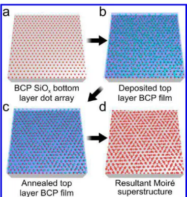
The general scheme for the self-assembly of incommensurate BCP double layers is shown inFigure 1. The bottom layer of hexagonal dots is formed via self-assembly of a PS-b-PDMS BCP, followed by solvent annealing and reactive ion etching (RIE) to transform the BCP into the nanopattern of silica dots (Figure 1a). A second layer of a PS-b-PDMS BCP, which has a different molecular weight and thus a different periodicity, is then spin-coated onto the initial pattern of silica dots (bottom layer). Upon a second solvent anneal (Figure 1c) and RIE treatment, the top layer of the PS-b-PDMS BCP is converted into another array of dots (Figure 1d). The resulting nanopattern is generally a moiré superstructure.
In this work, the two different PS-b-PDMS BCPs and BCP blend used in this study, and their abbreviations, are summarized inTable 1. These BCPs were chosen in order to explore a large range of array pitches and pitch ratios. The B30 blend was specifically chosen to achieve a large pitch of 43 nm (blending was necessary to produce dot arrays instead of cylindrical arrays).20 The plan view scanning electron micro-graphs (SEM) and atomic force micromicro-graphs (AFM) of single-layer silica dot patterns fabricated from B30, P43, and P22 on flat silicon substrates are shown in Figures S1 and S2
respectively, and the dot diameter, pitch, and height of each silica dot array are listed inTable 1. The layered structures are denoted by their deposition sequence. For example, P22-(bottom) + P43(top) is a sample where P22 is used as the bottom layer and P43 used as the top layer. The layered structures produced in this work are P22(bottom) + P43(top), P43(bottom) + P22(top), P43(bottom) + B30(top), and B30(bottom) + P43(top).
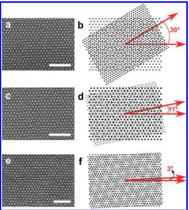
Examples of three moiré superstructures on flat silicon substrates, resulting from combinations of the BCPs listed in
Table 1, are shown inFigure 2.Figure 2a, c, and e show SEM micrographs of the three moiré superstructures, andFigure 2b, d, and f are schematic illustrations indicating the relative rotation of the individual dot arrays in the three moiré superstructures.Figure 2a and c utilize the same pair of BCPs, Figure 1. Schematic illustrating the method for formation of BCP dot-array-based moiré superstructures. (a) Formation of a bottom layer of hexagonal dots via self-assembly of a BCP, followed by solvent annealing and reactive ion etching (RIE) to transform the BCP into a hexagonal lattice of silica dots. (b) Deposition of a top layer BCP film on the preformed nanopattern of silica dots from (a). (c) Annealing of top layer BCP films results in orientational alignment of the top layer BCP dot array. (d) RIE of the top layer converts the BCP to silica dots, resulting in a moiré superstructure. Table 1. Pitch, Dot Diameter, and Height of Silica Nanodot Arrays Converted from the Annealed BCPs/BCP Blend Used in This Studya
abbreviation composition pitch (nm)/ HIM diameter (nm)/ SEM height (nm)/ AFM P22 PS-b-PDMS (22.5K− 4.5K) 23.4(5) 12.0(1.6) 2.9(4) P43 PS-b-PDMS (43K−8.5K) 34.1(6) 15.9(7) 5.0(4) B30 PS-b-PDMS (31.5K− 14.5K) + 30 wt % PS (10K) 42.5(5) 21.8(8) 7.3(5)
aSEM, HIM, and AFM refer to scanning electron microscopy, helium
but in reverse order, andFigure 2e examines a higher molecular weight BCP and a BCP/homopolymer blend. InFigure 2a the BCP with the lower molecular weight, P22 (PS-b-PDMS (22.5K−4.5K)), was applied as the bottom layer of dots, having a pitch of ∼23−24 nm (Table 1). The top layer of dots was formed from a higher molecular weight BCP, P43 (PS-b-PDMS (43K-8.5K)), which consequently has a larger pitch of ∼34 nm (Table 1). The resulting majority phase is shown inFigure 2a (vide infra for discussion of determination of majority phase). The relative rotation angle between the first and second layers is 30°. When carried out in the reverse order, with the bottom dot pattern formed from P43 formed, followed by P22 as the top layer, a different moiré superstructure is observed (majority phase,Figure 2c). The relative rotation angle between the two layers in this case is about 11°. Starting with P43 (pitch of ∼34 nm) as the bottom dot pattern, B30, which has a pitch of ∼42− 43 nm (Table 1), was used to form the top layer of dots; the majority phase of the resulting moiré superstructure is shown in
Figure 2e. In the latter case, the relative rotation angle between the two layers is near 3°.
Figure 3shows a representation of the individual layers in the three distinct majority phase moiré superstructures, as observed by SEM, in Figure 3a−c. The dots in Figure 3d−i were manually separated based on the differences in dot sizes between the two layers; the sizes of the dots are displayed as the average size of the corresponding BCP pattern determined from the SEM micrograph. The bottom layer dot nanopatterns,
Figure 3d−f, display long-range hexagonal ordering within the 850 nm × 850 nm area of the micrograph. The top layers,
Figure 3g−i, also show long-range hexagonal ordering despite
undergoing self-assembly on a surface with protruding silica dots of a different spacing. Figure 3j−l correspond to the original SEM micrographs in Figure 3a−c, with the layers stacked according to the annealing sequence: blue dots comprise the bottom layer and red dots the top layer. Random sampling via high-magnification SEM generally revealed a consistent moiré superstructure (majority phase) across the substrate. From these observations it was hypothesized that a unique set of preferential orientation relationship(s) exists between any two BCP dot arrays. However, from these micrographs it was also observed that there was some variance in the relative orientation of the lattices, as well as a sparse amount of other configurations.
In order to test the hypothesis of preferential lattice orientations, it was necessary to perform high-resolution large-area imaging of multiple films (made under identical processing conditions) in order to quantify the distributions of relative rotation between the two lattices, yielding statistically meaningful results. Helium ion microscopy (HIM) was used to acquire the high-resolution (8192 × 8192 pixels) large-scale micrographs [20 μm × 20 μm for P43(bottom) + B30(top), 15 μm × 15 μm for P22(bottom) + P43(top) and P43(bottom) + P22(top)]. From these micrographs, dot positions of the two layers in the moiré superstructures were separated using fast Fourier transform (FFT) filtering of the HIM images (see
Methodssection), and the orientations of each individual layer were calculated at each dot position using the data processing analyses, described in the Methods section. The relative orientations of the top and bottom layers were then calculated by taking the difference of these angles. Since the relative rotation angles are calculated per dot, those angles can be color mapped and plotted on the dot positions to form an image over the entire micrograph to reveal preferred domains, as well as other distinct superstructures. Examples of these processed images are shown in Figure 4, along with labeled details of these high-magnification images (Figure 4b−e and g−j) to reveal the nature of the moiré superstructures.Figure 4a and f are processed HIM micrographs of P43(bottom) + P22(top) and P43(bottom) + B30(top), respectively. As the hexagonal dot pattern has 6-fold circular symmetry, the relative rotation angle has been mapped on a cyclical color scale with a range of −30° to +30°. As can be seen upon close inspection ofFigure 4, the areas that have the same relative rotation, represented by the same colors, correspond to areas with the same patterns. These patterns have the same structure and relative rotation between the layers, although they do not have the same absolute rotation. It can be seen that these data are evidence of a preferential orientational relationship between the two layers. Shown in Figure 5 are spatial mappings of the lattice orientations for different bottom layers (a−c) and correspond-ing top layers (d−f). From these lattice orientation maps of the bottom and top layers, the relative rotation maps are calculated and shown inFigure 5g−i. The maps portray a 15 μm × 15 μm area of P22(bottom) + P43(top) and P43(bottom) + P22(top) and a 20 μm × 20 μm area of P43(bottom) + B30(top). The lattice angles are measured as described in theMethodssection from the horizontal axis of the image, where a color represents the lattice orientation as indicated by the cyclical color map, with a range of −30° to 30°. From these maps, the BCP dot pattern grains, grain orientations, and their associated grain boundaries are easily differentiated.
The relative rotation map for P43(bottom) + P22(top), shown inFigure 5h, indicates the presence of two phases with Figure 2. Left column: SEM micrographs of moiré superstructures
formed from sequential annealing of two incommensurate BCP combinations. Right column: corresponding schematic representa-tion. (a, b) P22(bottom) + P43(top). (c, d) P43(bottom) + P22(top). (e, f) P43(bottom) + B30(top). In (b), (d), and (f), the bottom layers are portrayed in black, and the top layers in gray. All scale bars are 250 nm.
ACS Nano Article
DOI:10.1021/acsnano.7b00322
ACS Nano2017, 11, 3237−3246
preferential rotation angles of −10 and +10 degrees. These patterns share the same moiré structure but have opposite chirality, as seen in the detailed dot patterns found inFigure 4c and g. Every preferential relative rotation angle at angles other than 0° or 30° will exhibit a selection between two degenerate lattice orientations, resulting in left- and right-handed domains of the same moiré structure, which on the chosen scale are seen as positive and negative angles of equal magnitude.45To clearly show the preferential relative rotation angles/lowest energy configuration of each sample, the absolute values of the relative rotation angles were plotted inFigure 5j−l. After accounting for the left- and right-handed domains, only the blue color, corresponding to an angle of about 10°, appears in the absolute relative rotation angle map in Figure 5k, revealing that the pattern has only one preferential dot configuration/moiré superstructure. Upon close inspection, all three samples show a preferred relative rotation angle and, thus, a preferred moiré superstructure. The preferential relative rotation angle between the two BCP layers of P22(bottom) + P43(top) is about 30° (Figure 5g and j). The relative rotation angle map and the absolute relative rotation map of P43(bottom) + B30(top) show a preferential relative rotation angle around 0°.
Inspection of the individual layers inFigure 5a−f shows that the grains of the top layer generally align with the bottom layer. However, as seen in the relative rotation maps (Figure 5g−i), the overlap of the grains is not perfect, as there are thin regions with very different relative lattice orientations. It is these grain boundary transition regions between the top and bottom layers that account for the different moiré superstructures occasionally observed in SEM (seeFigure S3).
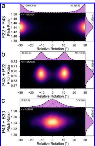
A moiré superstructure is uniquely defined by a pitch ratio (defined as the ratio of the dot pitch of the top layer divided by that of the bottom layer) and a relative rotation between the layers. As such, in order to analyze the moiré structures found in these samples, the distributions of these quantities are shown in Figure 6, which are calculated using a 2D and 1D kernel density estimation (KDE).72 Each chart is an ensemble of statistics from multiple HIM micrographs and samples, with the total number of dots indicated in the KDE as N. The median pitch ratios and relative rotation angles of five different configurations of sequentially deposited BCP bilayers are summarized in Table 2. The native pitch ratio is also listed, which is defined as the ratio of dot spacings found in the corresponding single (or bottom) layer patterns. The dot pitch distributions of the dot patterns from the separated layers can be seen inFigure S4. Two additional configurations are listed in the table, B30(bottom) + P43(top) and B30oe(bottom) + P43(top), which will be discussed later.
Several observations can be made from these KDEs. First, for any given configuration, it is seen that all relative rotations are clustered around an angle of θ0and −θ0(which corresponds to the chiral but degenerate moiré superstructure), with standard deviations on the order of ∼3.5°. These data substantiate the hypothesis that preferred moiré superstructure(s) can be formed for a given pair of incommensurate BCP lattices, further suggesting that these moiré superstructures represent a minima in the energy landscape of these incommensurate BCP lattices. Inspection ofTable 2reveals that differences in native and measured pitch ratio are between 0 and 2%. These data imply that the registration force from the bottom layer is insufficiently strong to induce a large global strain of the top Figure 3. Separation of BCP moiré superstructures into top and bottom layers. (a−c) SEM micrographs, (d−f) dot patterns of the bottom layer, (g−i) dot patterns of the top layer, (j−l) combined bottom and top layers of the three moiré superstructures. All scale bars are 250 nm.
layer lattice spacing. Lastly, the 2D KDEs show little correlation between the measured pitch ratio and the relative rotation, seen by the on-axial orientation of the elliptical peak shape and the near-zero Pearson product-moment correlation coefficients found inTable 2. This result suggests that local variations in relative lattice orientation do not significantly modify the local pitch ratio.
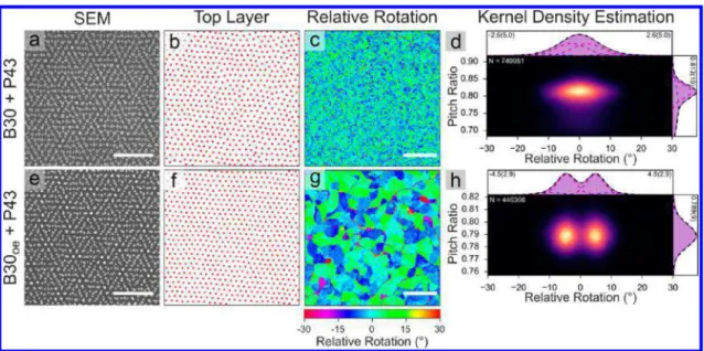
In addition to the previous three BCP combinations, B30(bottom) + P43(top) was also produced. However, the resulting pattern formed by this combination, shown inFigure 7a−d,Figure S5a−d, and Figure S6a−d, differs significantly. In contrast to the other three examples analyzed, the spherical micelle domains of the top layer, P43, tend to deviate from their equilibrium lattice positions, having a higher density of point defects, which can be clearly seen via the dot separation inFigure 7b. Interestingly, despite the higher defect density in the top layer of P43, there is still a preferential orientational relationship between the top and bottom layers. As seen in
Figure 7d, the distribution of relative rotation angles is consistently centered around 0°, although quite broad with respect to both pitch and angle. The relative rotation is fit with two peaks at angles of ±2.6(5.0)°. Two peaks were used because the resulting pattern has areas that twist from ∼0° to ∼+5° and others that twist from ∼0° to ∼−5°, as can be clearly
seen inFigure 7c, where there are distinct regions of green and blue, as opposed to a uniform mixture of the two colors. The different registration observed in this system may be due to the size of the silica dots derived from the B30 BCP blend, which produces dots with a height of 7.3 nm and a rather large diameter of 21.8 nm compared to the dots derived from P43, which have a height of 5 nm and a diameter of 15.9 nm.
To further study the effects of bottom layer dot size on the epitaxy of the top layer, the first layer of the B30 silica dots was etched by RIE with an extra 5 s of CF4(100 mT, 50 W) to reduce the dot size to 5.2 nm in height and 18.2 nm in diameter (Figure S7). This configuration is defined as B30oe(bottom) + P43(top).Figure 7e−h shows the resulting pattern and analysis of the registration of the top layer formed from P43 on B30oe. The epitaxial registration of the top layer on B30oe is remarkably different when compared to the previous B30-(bottom) + P43(top) sample. One of the most striking differences is the dramatic increase of long-range ordering observed in the top layer (compareFigure 7b and f). Second, the distribution of the relative rotation angles between the top and bottom layers has two clearly defined peaks centered at +5° and −5° (Figure 7d and h). Moreover, the relative rotation map of B30oe(bottom) + P43(top) (Figure 7g) appears to be much more similar to the other BCP combinations used in this work Figure 4. Large-area high-magnification map of relative lattice orientation between top and bottom BCP dot arrays. (a) Relative rotation angles of the bottom and top dot layers, derived from P43(bottom) + P22(top), as defined as the angular difference between the lattice orientation of the two dot patterns. In this map, a single color corresponds to a particular moiré superstructure. (b−e) Higher magnification of (a) as labeled. (f) Dot lattice relative rotation angles in the combination of P43(bottom) + B30(top). (g−j) Higher magnification of (f) as labeled.
ACS Nano Article
DOI:10.1021/acsnano.7b00322
ACS Nano2017, 11, 3237−3246
(Figure 5), where there are large micrometer-sized regions possessing a single relative orientation, which are delineated by grain boundaries of either the top or bottom layer. Unlike B30(bottom) + P43(top), the 2D KDE of B30oe(bottom) + P43(top) (Figure 7h) shows two well-resolved peaks. The relative rotation angle between the top P43 layer and the bottom B30oe is fit to 4.8(2.9)°. The pitch ratio of B30oe(bottom) + P43(top) was measured to be 0.803(17), which is very close to the native pitch ratio (Table 2). These results indicate that the pitch ratio is not the only parameter that determines that resultant structure, as the relative dot sizes can also strongly influence the final morphology. In this case, as the dot size of the bottom layer is reduced, the registration with the top layer weakens. At these smaller dot sizes, the registration is insufficient to create point defects in the top layer, but is sufficiently strong such that the configurational energy is minimized with a relative rotation of ±5°. Similar observations have also been reported in a study of self-assembly of PS-b-PDMS cylinders over silica pillar arrays, formed via e-beam lithography of HSQ.73 In that work, differences in the silica post height of as little as 3 nm, in the range of 12 to 26 nm, induced substantial changes in the morphology and orientation of the self-assembled microdomains of the PS-b-PDMS BCP. Similar to the observations presented in this work, the phenomenon of preferential orientation between two different hexagonal lattices has also been widely reported for the alignment of hard two-dimensional atomic materials. Specifically, graphene on hexagonal boron nitride (hBN),74 hBN on Ir(111),75 graphene on Ir(111),76 and graphene on
transition metal surfaces77 show well-defined preferred orientations. These resulting configurations are found to be
reasonably well predicted by a simple two-dimensional model, where the configurational energy of all possible moiré superstructures can be estimated for any pair of infinitely large defect-free hexagonal lattices.78Unfortunately, this model fails to predict the majority of experimentally observed configurations for the BCP lattices investigated in this work. In order to properly predict the moiré superstructures between BCP dot lattices, a much more sophisticated model is necessary. Specifically, the three-dimensional geometrical nature of these structures is fundamentally important, which is clearly illustrated inFigure 7, where a 2 nm reduction in dot height significantly altered the observed moiré structure. Moreover, the significant deviations from ideal hexagonal positions (in all three spatial dimensions) for BCP dot arrays will play an important role in the energy minimization. As such, it is believed that simulation methods such as self-consistent field theory (SCFT) or molecular dynamics (MD) are necessary to predict and more deeply understand the formation of these BCP moiré superstructures. It is also emphasized that these simulations will have been done over a very large simulation volume to account for low-angle moiré patterns, domain size effects, and deviations from ideal positions for the bottom registration lattice.
CONCLUSIONS
Sequential self-assembly of incommensurate BCP dot arrays leads to preferred orientations, thus providing a route toward a unique set of large-area, single-grain moiré superstructures. The registration force of the bottom layer of dots is sufficiently strong to bring about registration of the top layer, resulting in formation of a majority phase. The advantages of nano-Figure 5. Grain structures of top and bottom layers and corresponding relative orientations between layers. (a−f) Bottom and top layer dot-pattern lattice orientations (relative to the horizontal axis of the image). (g−i) Relative rotation angle between dot dot-patterns of the first and second layers as described inFigure 4. (j−l) Absolute values of previous relative rotation angles showing the chiral symmetry resulting from the degenerate lattice orientations in the double-layer patterns. All scale bars are 5 μm in length. Interactive and full-resolution images of all of these maps can be found online athttp://maverick.chem.ualberta.ca/bcp_micrographs/using the Web Deep Zoom Toolkit developed at NIST.71
lithography via self-assembly of BCPs are multifold and include the low cost of processing, their high resolution, and well-developed methods to transfer the BCP nanopattern to the underlying substrate. This class of registration between BCP layers suggests an avenue to access a complex family of patterns and motifs, through an entirely bottom-up process. As is always
the case with nanopatterning via self-assembly of BCPs, subtle effects are important, including the critical role of dot size, grain boundaries between dot domains, and the annealing process. Further investigation into the fundamental aspects of self-assembly of the second layer during the annealing step, coupled with large-scale statistical analysis of the resulting patterns, will lead to a better understanding of registration and, hence, reduce the level of defects in the resulting nanopatterns.
METHODS
Materials. All BCPs (PDMS (31K-14.5K), PDI 1.15; PS-b-PDMS (43K-8.5K), PDI 1.04; PS-b-PS-b-PDMS (22.5K-4.5K), PDI 1.09) and polystyrene (PS) (10K, PDI 1.09) were obtained from Polymer Source Inc. Toluene and tetrahydrofuran (THF) were purchased from Fisher Scientific. Silicon wafers (⟨100⟩, 4 in. diameter, thickness 525 ± 25 μm, p-type (boron doped), resistivity < 0.005 Ω·cm) were purchased from WRS Materials. Sulfuric acid (96%) and hydrogen peroxide (30%) were purchased from Avantor Performance Materials. Silicon Wafer Dicing and Cleaning. Silicon wafers were diced into 1 cm × 1 cm squares by a DSA 321 dicing saw and cleaned with piranha solution [3:1 v/v sulfuric acid (96%)/hydrogen peroxide (30%)].
Imaging. All images were taken with a Hitachi S4800 scanning electron microscope (15 kV, 20 μA), a Zeiss scanning helium ion beam microscope (30.8 kV, 10 μm aperture, spot size 4), or atomic force microscope (Digital Instruments/Veeco, tapping mode under ambient condition).
BCP Thin-Film Self-Assembly and Reactive Ion Etching.The general experimental procedure used in this work of sequential annealing of block copolymer thin films and conversion into silica dot patterns is shown inFigure 1. A detailed description of BCP thin-film preparation, annealing procedure, annealing conditions, etching recipes for each BCP sample, and sequential annealing procedures can be found in previous papers.68,79Briefly, the fabrication process begins by spin-casting a dot-forming BCP or BCP/PS blend thin film (bottom layer) on piranha-cleaned 1 cm × 1 cm silicon chips from a 1 wt % toluene solution. For each BCP or BCP/PS blend, the film thickness was optimized to form a single-layer dot pattern after solvent annealing. In this paper, three different BCPs and a BCP/PS blend were used, PS-b-PDMS (13K−14.5K)/30 wt % PS (denoted as B30), PS-b-PDMS (43K−8.5K) (denoted as P43), and PS-b-PDMS (22.5K− 4.5K) (denoted as P22). The optimized film thicknesses for B30, P43, and P22 were ∼32, ∼30, and ∼25 nm, respectively. The BCP or BCP/ PS blended films were annealed in a custom-made solvent annealing chamber, where THF was used as the annealing solvent.68,79 Film
thickness was monitored in situ during the annealing process using ellipsometry (λ = 632.8 nm, θ = 70°). The optimized final swelling degrees (swollen film thickness/initial film thickness) of each sample were ∼2.0 for B30 and P43 and ∼1.6 for P22. After annealing, hexagonally packed spherical PDMS domains were bound within the PS matrix. The annealed BCP or BCP/PS blend films were then converted to a silica dot array by applying a CF4/O2RIE treatment (Figure 1a). The etching recipe for each BCP film can also be found in our previous paper.68 During RIE etching, the PDMS domains are oxidized to SiOx, and PS domains are etched away. Following the first patterning step, the top layer of the BCP or BCP/PS blend thin film was then spin-cast onto the now-patterned silicon substrate (Figure 1b). The top layer of the BCP film was annealed and converted to silica dots using identical annealing and RIE conditions as those of the bottom layer.
Data Processing.Statistical analyses of lattice angles and dot pitch were taken from a collection of HIM micrographs with a 15 or 20 μm field of view and a resolution of 8192 × 8192 pixels (1.8 or 2.4 nm/ pixel, respectively). The statistical analysis of P22(bottom) + P43(top) was carried out using eight HIM micrographs (15 μm × 15 μm) from three different samples comprising over 1.6 million dots. P43(bottom) + P22(top) statistics were collected from 10 HIM micrographs (15 μm ×15 μm) from three different samples comprising over 1.9 million dots. P43(bottom) + B30(top) statistics were collected from five HIM Figure 6. 2D and 1D kernel density estimations showing the
distribution of pitch ratios (L2/L1) and relative rotation angles found in the moiré superstructures. (a) Statistical representation of P22(bottom) + P43(top) comprising 8 HIM micrographs (15 μm ×15 μm) from three different samples, sampling a total of over 1.6 million dots. (b) Statistical representation of P43(bottom) + P22(top) comprising 10 HIM micrographs (15 μm × 15 μm) from three different samples, sampling a total of over 1.9 million dots. (c) Statistical representation of P43(bottom) + B30(top) comprising 5 HIM micrographs (20 μm × 20 μm) from one sample, containing over 0.9 million dots.
Table 2. Native Pitch Ratios Calculated from Bottom Layer HIM Data, Pitch Ratios (L2/L1), Relative Rotation Angles, and the Correlation Coefficients between the Pitch Ratio and Absolute Relative Rotation Angle for the Resulting Moiré Superstructuresa
BCP layers (bottom +
top) ratio (L2/L1)native pitch measured pitchratio (L2/L1)
relative rotation
(deg) correlationcoefficient P22 + P43 1.46(4) 1.443(21) 29.9(3.6) 0.007 P43 + P22 0.687(19) 0.695(10) 10.7(3.3) 0.018 P43 + B30 1.245(27) 1.245(16) 3.3(3.8) 0.045 B30 + P43 0.803(17) 0.813(19) 2.6(5.0) −0.004 B30oe+ P43 0.803(17) 0.789(9) 4.8(2.9) −0.007 aB30
oerefers to a B30 sample that was overetched by RIE to decrease dot size. The listed uncertainties are the measured standard deviations of each quantity.
ACS Nano Article
DOI:10.1021/acsnano.7b00322
ACS Nano2017, 11, 3237−3246
micrographs (20 μm × 20 μm) from one sample comprising over 0.9 million dots. P43(bottom) + B30(top) statistics were collected from four HIM micrographs (20 μm × 20 μm) from one sample comprising over 0.7 million dots. The dot positions corresponding to the top and bottom BCP layers were separated via Fourier filtering using Gwyddion analysis software.80 Specifically, due to the differences in dot pitch (L0) of each layer, the dots from a single layer (either top or bottom) can be revealed by application of a bandpass filter centered on the fundamental frequency of each lattice (k ≃ 2/√3L0−1). Dot positions were then determined by a thresholding algorithm (Ostu’s method). It is noted that this type of separation is possible only on patterns that do not have overlapping fundamental frequencies.
To measure the pitch and angle of each dot, the positions of the six nearest neighbors of each dot were first determined. The pitch of each dot was then taken as the mean distance between the central dot and its six nearest neighbors. The lattice angle of each dot was defined as the orientation of the corresponding coordination shell of each dot, relative to the horizontal axis of the image; this was determined by calculating the angle between the central dot and each of its coordinating dots (modulo 60°). The circular mean of these six angles was then used to calculate the lattice orientation.
ASSOCIATED CONTENT
*
S Supporting InformationThe Supporting Information is available free of charge on the
ACS Publications websiteat DOI:10.1021/acsnano.7b00322. SEM and AFM micrographs of single-layer BCP dot arrays, SEM characterization and analysis of grain boundaries between moiré superstructures, distributions of dot pitches for top and bottom layers, analysis of moiré structures with an overetched bottom layer, and distributions of dot height (PDF)
AUTHOR INFORMATION Corresponding Authors *E-mail: [email protected]. *E-mail: [email protected]. ORCID Jillian M. Buriak: 0000-0002-9567-4328 Notes
The authors declare no competing financial interest. ACKNOWLEDGMENTS
This work was supported by grants from the Natural Sciences and Engineering Research Council (NSERC, grant numbers RGPIN-283291-09, RGPIN-2014-05195), Alberta Innovates Technology Futures (fellowship to C.J. and grant number AITF iCORE IC50-T1 G2013000198), and the Canada Research Chairs Program (CRC 207142). Helium ion microscopy was carried out in the University of Alberta’s Centre for Nanofabrication (nanoFAB), and SEM at NRC-NINT. Assistance from the nanoFAB staff is gratefully acknowledged. REFERENCES
(1) Bates, F. S.; Fredrickson, G. H. Block Copolymer Thermody-namics: Theory and Experiment. Annu. Rev. Phys. Chem. 1990, 41, 525−557.
(2) International Technology Roadmap for Semiconductors; 2011; Semiconductor Industry Association: San Jose, CA, 2011.http://www. itrs2.net/.
(3) Luo, M.; Epps, T. H. Directed Block Copolymer Thin Film Self-Assembly: Emerging Trends in Nanopattern Fabrication.
Macro-molecules 2013, 46, 7567−7579.
(4) Ji, S.; Wan, L.; Liu, C.-C.; Nealey, P. F. Directed Self-Assembly of Block Copolymers on Chemical Patterns: A Platform for Nano-fabrication. Prog. Polym. Sci. 2016, 5455, 76−127.
(5) Harriott, L. R. Limits of Lithography. Proc. IEEE 2001, 89, 366− 374.
(6) Hadjichristidis, N.; Pispas, S.; Floudas, G. Block Copolymers:
Synthetic Strategies, Physical Properties, and Applications, 1st ed.;
Wiley-Interscience: Hoboken, NJ, 2002.
(7) Bates, C. M.; Bates, F. S. 50th Anniversary Perspective: Block Polymers. Macromolecules 2017, 50, 3−22.
(8) Segalman, R. A. Patterning with Block Copolymer Thin Films.
Mater. Sci. Eng., R 2005, 48, 191−226.
(9) Darling, S. B. Directing the Self-Assembly of Block Copolymers.
Prog. Polym. Sci. 2007, 32, 1152−1204.
(10) Sinturel, C.; Vayer, M.; Morris, M.; Hillmyer, M. A. Solvent Vapor Annealing of Block Polymer Thin Films. Macromolecules 2013,
46, 5399−5415.
Figure 7. Effect of bottom layer dot size on the resulting moiré superstructures. (a−d) Data for the B30(bottom) + P43(top) BCP moiré superstructures. (e−h) Data for a B30oe(bottom) + P43(top) moiré superstructures where the bottom B30 BCP layer was etched by RIE for an extra 5 s, resulting in the formation of smaller silica dots. Scale bars in SEM micrographs (a, b, e, and f) are 250 nm, and scale bars in the relative rotation angle maps (c and g) are 5 μm in length.
(11) Li, W.; Liu, M.; Qiu, F.; Shi, A.-C. Phase Diagram of Diblock Copolymers Confined in Thin Films. J. Phys. Chem. B 2013, 117, 5280−5288.
(12) Park, M. Block Copolymer Lithography: Periodic Arrays of ∼ 1011Holes in 1 Square Centimeter. Science 1997, 276, 1401−1404.
(13) Tang, C.; Lennon, E. M.; Fredrickson, G. H.; Kramer, E. J.; Hawker, C. J. Evolution of Block Copolymer Lithography to Highly Ordered Square Arrays. Science 2008, 322, 429−432.
(14) Cummins, C.; Ghoshal, T.; Holmes, J. D.; Morris, M. A. Strategies for Inorganic Incorporation Using Neat Block Copolymer Thin Films for Etch Mask Function and Nanotechnological Application. Adv. Mater. 2016, 28, 5586−5618.
(15) Gu, X.; Gunkel, I.; Russell, T. P. Pattern Transfer Using Block Copolymers. Philos. Trans. R. Soc., A 2013, 371, 20120306.
(16) Aizawa, M.; Buriak, J. M. Block Copolymer-Templated Chemistry on Si, Ge, InP, and GaAs Surfaces. J. Am. Chem. Soc. 2005, 127, 8932−8933.
(17) Chai, J.; Buriak, J. M. Using Cylindrical Domains of Block Copolymers To Self-Assemble and Align Metallic Nanowires. ACS
Nano 2008, 2, 489−501.
(18) Chaudhari, A.; Ghoshal, T.; Shaw, M. T.; O’Connell, J.; Kelly, R. A.; Glynn, C.; O’Dwyer, C.; Holmes, J. D.; Morris, M. A. Fabrication of MoS2 Nanowire Arrays and Layered Structures via the Self-Assembly of Block Copolymers. Adv. Mater. Interfaces 2016, 3, 1500596.
(19) Wei, W.; Samad, L.; Choi, J. W.; Joo, Y.; Way, A.; Arnold, M. S.; Jin, S.; Gopalan, P. Synthesis of Molybdenum Disulfide Nanowire Arrays Using a Block Copolymer Template. Chem. Mater. 2016, 28, 4017−4023.
(20) Wu, N. L. Y.; Harris, K. D.; Buriak, J. M. Conversion of Bilayers of PS-B-PDMS Block Copolymer into Closely Packed, Aligned Silica Nanopatterns. ACS Nano 2013, 7, 5595−5606.
(21) Wu, N. L. Y.; Zhang, X.; Murphy, J. N.; Chai, J.; Harris, K. D.; Buriak, J. M. Density Doubling of Block Copolymer Templated Features. Nano Lett. 2012, 12, 264−268.
(22) Nunns, A.; Gwyther, J.; Manners, I. Inorganic Block Copolymer Lithography. Polymer 2013, 54, 1269−1284.
(23) Liang, C. D.; Hong, K. L.; Mays, J. W.; Dai, S. Synthesis of a Large-Scale Highly Ordered Porous Carbon Film by Self-Assembly of Block Copolymers. Angew. Chem., Int. Ed. 2004, 43, 5785−5789.
(24) Werner, J. G.; Hoheisel, T. N.; Wiesner, U. Synthesis and Characterization of Gyroidal Mesoporous Carbons and Carbon Monoliths with Tunable Ultralarge Pore Size. ACS Nano 2013, 8, 731−743.
(25) Bates, C. M.; Maher, M. J.; Janes, D. W.; Ellison, C. J.; Willson, C. G. Block Copolymer Lithography. Macromolecules 2014, 47, 2−12. (26) Singh, G.; Batra, S.; Zhang, R.; Yuan, H.; Yager, K. G.; Cakmak, M.; Berry, B.; Karim, A. Large-Scale Roll-to-Roll Fabrication of Vertically Oriented Block Copolymer Thin Films. ACS Nano 2013, 7, 5291−5299.
(27) Griffiths, R. A.; Williams, A.; Oakland, C.; Roberts, J.; Vijayaraghavan, A.; Thomson, T. Directed Self-Assembly of Block Copolymers for Use in Bit Patterned Media Fabrication. J. Phys. D:
Appl. Phys. 2013, 46, 503001.
(28) Trawick, M.; Angelescu, D.; Chaikin, P.; Register, R. Block Copolymer Nanolithography. In Nanolithography and Patterning
Techniques in Microelectronics; Elsevier, 2005; pp 1−38.
(29) Ouk Kim, S.; Solak, H. H.; Stoykovich, M. P.; Ferrier, N. J.; de Pablo, J. J.; Nealey, P. F. Epitaxial Self-Assembly of Block Copolymers on Lithographically Defined Nanopatterned Substrates. Nature 2003,
424, 411−414.
(30) Cheng, J. Y.; Ross, C. A.; Smith, H. I.; Thomas, E. L. Templated Self-Assembly of Block Copolymers: Top-Down Helps Bottom-Up.
Adv. Mater. 2006, 18, 2505−2521.
(31) Black, C. T.; Ruiz, R.; Breyta, G.; Cheng, J. Y.; Colburn, M. E.; Guarini, K. W.; Kim, H. C.; Zhang, Y. Polymer Self Assembly in Semiconductor Microelectronics. IBM J. Res. Dev. 2007, 51, 605−633. (32) Ruiz, R.; Kang, H.; Detcheverry, F. A.; Dobisz, E.; Kercher, D. S.; Albrecht, T. R.; Pablo, J. J. de; Nealey, P. F. Density Multiplication
and Improved Lithography by Directed Block Copolymer Assembly.
Science 2008, 321, 936−939.
(33) Park, S.; Lee, D. H.; Xu, J.; Kim, B.; Hong, S. W.; Jeong, U.; Xu, T.; Russell, T. P. Macroscopic 10-Terabits-per-Inch Arrays from Block Copolymers with Lateral Order. Science 2009, 323, 1030−1033.
(34) Kim, H.-C.; Park, S.-M.; Hinsberg, W. D. Block Copolymer Based Nanostructures: Materials, Processes, and Applications to Electronics. Chem. Rev. 2010, 110, 146−177.
(35) Kim, S.; Shin, D. O.; Choi, D.-G.; Jeong, J.-R.; Mun, J. H.; Yang, Y.-B.; Kim, J. U.; Kim, S. O.; Jeong, J.-H. Graphoepitaxy of Block-Copolymer Self-Assembly Integrated with Single-Step ZnO Nano-imprinting. Small 2012, 8, 1563−1569.
(36) Kim, E.; Ahn, H.; Park, S.; Lee, H.; Lee, M.; Lee, S.; Kim, T.; Kwak, E.-A.; Lee, J. H.; Lei, X.; Huh, J.; Bang, J.; Lee, B.; Ryu, D. Y. Directed Assembly of High Molecular Weight Block Copolymers: Highly Ordered Line Patterns of Perpendicularly Oriented Lamellae with Large Periods. ACS Nano 2013, 7, 1952−1960.
(37) Hardy, C. G.; Tang, C. Advances in Square Arrays Through Self-Assembly and Directed Self-Assembly of Block Copolymers. J.
Polym. Sci., Part B: Polym. Phys. 2013, 51, 2−15.
(38) Ross, C. A.; Berggren, K. K.; Cheng, J. Y.; Jung, Y. S.; Chang, J.-B. Three-Dimensional Nanofabrication by Block Copolymer Self-Assembly. Adv. Mater. 2014, 26, 4386−4396.
(39) Maher, M. J.; Rettner, C. T.; Bates, C. M.; Blachut, G.; Carlson, M. C.; Durand, W. J.; Ellison, C. J.; Sanders, D. P.; Cheng, J. Y.; Willson, C. G. Directed Self-Assembly of Silicon-Containing Block Copolymer Thin Films. ACS Appl. Mater. Interfaces 2015, 7, 3323− 3328.
(40) Deng, H.; Xie, N.; Li, W.; Qiu, F.; Shi, A.-C. Perfectly Ordered Patterns via Corner-Induced Heterogeneous Nucleation of Self-Assembling Block Copolymers Confined in Hexagonal Potential Wells. Macromolecules 2015, 48, 4174−4182.
(41) Morris, M. A. Directed Self-Assembly of Block Copolymers for Nanocircuitry Fabrication. Microelectron. Eng. 2015, 132, 207−217.
(42) Yi, H.; Bao, X.-Y.; Zhang, J.; Bencher, C.; Chang, L.-W.; Chen, X.; Tiberio, R.; Conway, J.; Dai, H.; Chen, Y.; Mitra, S.; Wong, H.-S. P. Flexible Control of Block Copolymer Directed Self-Assembly Using Small, Topographical Templates: Potential Lithography Solution for Integrated Circuit Contact Hole Patterning. Adv. Mater. 2012, 24, 3107−3114.
(43) Jeong, J. W.; Hur, Y. H.; Kim, H.-j.; Kim, J. M.; Park, W. I.; Kim, M. J.; Kim, B. J.; Jung, Y. S. Proximity Injection of Plasticizing Molecules to Self-Assembling Polymers for Large-Area, Ultrafast Nanopatterning in the Sub-10-nm Regime. ACS Nano 2013, 7, 6747− 6757.
(44) Xiao, S.; Yang, X.; Steiner, P.; Hsu, Y.; Lee, K.; Wago, K.; Kuo, D. Servo-Integrated Patterned Media by Hybrid Directed Self-Assembly. ACS Nano 2014, 8, 11854−11859.
(45) Bita, I.; Yang, J. K. W.; Jung, Y. S.; Ross, C. A.; Thomas, E. L.; Berggren, K. K. Graphoepitaxy of Self-Assembled Block Copolymers on Two-Dimensional Periodic Patterned Templates. Science 2008, 321, 939−943.
(46) Hong, S. W.; Gu, X.; Huh, J.; Xiao, S.; Russell, T. P. Circular Nanopatterns over Large Areas from the Self-Assembly of Block Copolymers Guided by Shallow Trenches. ACS Nano 2011, 5, 2855− 2860.
(47) Kim, K.; Park, S.; Kim, Y.; Bang, J.; Park, C.; Ryu, D. Y. Optimized Solvent Vapor Annealing for Long-Range Perpendicular Lamellae in PS-b-PMMA Films. Macromolecules 2016, 49, 1722−1730. (48) Stoykovich, M. P.; Müller, M.; Kim, S. O.; Solak, H. H.; Edwards, E. W.; Pablo, J. J. de; Nealey, P. F. Directed Assembly of Block Copolymer Blends into Nonregular Device-Oriented Structures.
Science 2005, 308, 1442−1446.
(49) Stoykovich, M. P.; Kang, H.; Daoulas, K. C.; Liu, G.; Liu, C.-C.; de Pablo, J. J.; Müller, M.; Nealey, P. F. Directed Self-Assembly of Block Copolymers for Nanolithography: Fabrication of Isolated Features and Essential Integrated Circuit Geometries. ACS Nano 2007, 1, 168−175.
ACS Nano Article
DOI:10.1021/acsnano.7b00322
ACS Nano2017, 11, 3237−3246
(50) Park, S.-M.; Craig, G. S. W.; La, Y.-H.; Solak, H. H.; Nealey, P. F. Square Arrays of Vertical Cylinders of PS-b-PMMA on Chemically Nanopatterned Surfaces. Macromolecules 2007, 40, 5084−5094.
(51) Tavakkoli, A. T. K.; Nicaise, S. M.; Gadelrab, K. R.; Alexander-Katz, A.; Ross, C. A.; Berggren, K. K. Multilayer Block Copolymer Meshes by Orthogonal Self-Assembly. Nat. Commun. 2016, 7, 10518. (52) Tavakkoli, K. G.; Gotrik, K. W.; Hannon, A. F.; Alexander-Katz, A.; Ross, C. A.; Berggren, K. K. Templating Three-Dimensional Self-Assembled Structures in Bilayer Block Copolymer Films. Science 2012,
336, 1294−1298.
(53) Nicaise, S. M.; Amir Tavakkoli, K. G.; Berggren, K. K. 8 - Self-Assembly of Block Copolymers by Graphoepitaxy A2 - Gronheid, Roel. In Directed Self-assembly of Block Co-polymers for
Nano-manufacturing; Nealey, P., Ed.; Woodhead publishing series in
electronic and optical materials; Woodhead Publishing, 2015; pp 199−232.
(54) Nagpal, U.; Kang, H.; Craig, G. S. W.; Nealey, P. F.; de Pablo, J. J. Pattern Dimensions and Feature Shapes of Ternary Blends of Block Copolymer and Low Molecular Weight Homopolymers Directed To Assemble on Chemically Nanopatterned Surfaces. ACS Nano 2011, 5, 5673−5682.
(55) Tada, Y.; Yoshida, H.; Ishida, Y.; Hirai, T.; Bosworth, J. K.; Dobisz, E.; Ruiz, R.; Takenaka, M.; Hayakawa, T.; Hasegawa, H. Directed Self-Assembly of POSS-Containing Block Copolymer on Lithographically Defined Chemical Template with Morphology Control by Solvent Vapor. Macromolecules 2012, 45, 292−304.
(56) Xiao, S.; Yang, X.; Lee, K. Y.; Hwu, J. J.; Wago, K.; Kuo, D. Directed Self-Assembly for High-Density Bit-Patterned Media Fabrication Using Spherical Block Copolymers. J. Micro/Nanolithogr.,
MEMS, MOEMS 2013, 12, 031110−031110.
(57) Son, J. G.; Chang, J.-B.; Berggren, K. K.; Ross, C. A. Assembly of Sub-10-nm Block Copolymer Patterns with Mixed Morphology and Period Using Electron Irradiation and Solvent Annealing. Nano Lett. 2011, 11, 5079−5084.
(58) Yang, X.; Xiao, S.; Hsu, Y.; Feldbaum, M.; Lee, K.; Kuo, D. Directed Self-Assembly of Block Copolymer for Bit Patterned Media with Areal Density of 1.5 Teradot/Inch2and Beyond. J. Nanomater. 2013, 2013, e615896.
(59) Cheng, J. Y.; Mayes, A. M.; Ross, C. A. Nanostructure Engineering by Templated Self-Assembly of Block Copolymers. Nat.
Mater. 2004, 3, 823−828.
(60) Park, W. I.; Kim, K.; Jang, H.-I.; Jeong, J. W.; Kim, J. M.; Choi, J.; Park, J. H.; Jung, Y. S. Directed Self-Assembly with Sub-100 Degrees Celsius Processing Temperature, Sub-10 Nanometer Resolution, and Sub-1 minute Assembly Time. Small 2012, 8, 3762−3768.
(61) Salaun, M.; Zelsmann, M.; Archambault, S.; Borah, D.; Kehagias, N.; Simao, C.; Lorret, O.; Shaw, M. T.; Torres, C. M. S.; Morris, M. A. Fabrication of Highly Ordered Sub-20 nm Silicon Nanopillars by Block Copolymer Lithography Combined with Resist Design. J. Mater.
Chem. C 2013, 1, 3544−3550.
(62) Choi, Y. J.; Kim, J. Y.; Kim, J. E.; Mun, J. H.; Cha, S. K.; Kim, S. O. Hierarchical Directed Self-Assembly of Diblock Copolymers for Modified Pattern Symmetry. Adv. Funct. Mater. 2016, 26, 6462−6470. (63) Jung, Y. S.; Chang, J. B.; Verploegen, E.; Berggren, K. K.; Ross, C. A. A Path to Ultranarrow Patterns Using Self-Assembled Lithography. Nano Lett. 2010, 10, 1000−1005.
(64) Choi, J.; Huh, J.; Carter, K. R.; Russell, T. P. Directed Self-Assembly of Block Copolymer Thin Films Using Minimal Topo-graphic Patterns. ACS Nano 2016, 10, 7915−7925.
(65) Shin, D. O.; Mun, J. H.; Hwang, G.-T.; Yoon, J. M.; Kim, J. Y.; Yun, J. M.; Yang, Y.-B.; Oh, Y.; Lee, J. Y.; Shin, J.; Lee, K. J.; Park, S.; Kim, J. U.; Kim, S. O. Multicomponent Nanopatterns by Directed Block Copolymer Self-Assembly. ACS Nano 2013, 7, 8899−8907.
(66) Polleux, J.; Rasp, M.; Louban, I.; Plath, N.; Feldhoff, A.; Spatz, J. P. Benzyl Alcohol and Block Copolymer Micellar Lithography: A Versatile Route to Assembling Gold and in Situ Generated Titania Nanoparticles into Uniform Binary Nanoarrays. ACS Nano 2011, 5, 6355−6364.
(67) Rahman, A.; Majewski, P. W.; Doerk, G.; Black, C. T.; Yager, K. G. Non-Native Three-Dimensional Block Copolymer Morphologies.
Nat. Commun. 2016, 7, 13988.
(68) Jin, C.; Olsen, B. C.; Wu, N. L. Y.; Luber, E. J.; Buriak, J. M. Sequential Nanopatterned Block Copolymer Self-Assembly on Surfaces. Langmuir 2016, 32, 5890−5898.
(69) Luchnikov, V.; Kondyurin, A.; Formanek, P.; Lichte, H.; Stamm, M. Moiré Patterns in Superimposed Nanoporous Thin Films Derived from Block-Copolymer Assemblies. Nano Lett. 2007, 7, 3628−3632.
(70) Chen, K.; Rajeeva, B. B.; Wu, Z. L.; Rukavina, M.; Dao, T. D.; Ishii, S.; Aono, M.; Nagao, T.; Zheng, Y. B. Moiré Nanosphere Lithography. ACS Nano 2015, 9, 6031−6040.
(71) Vandecreme, A.; Blattner, T.; Majurski, M.; Bajcsy, P.; Scott, K.; Scott, J. H. J. From Image Tiles to Web-Based Interactive Measurements in One Stop. Microsc. Microanal. 2015, 21, 89−90.
(72) Scott, D. W. Multivariate Density Estimation: Theory, Practice,
and Visualization, 1st ed..; Wiley: New York, 1992.
(73) Chang, J.-B.; Son, J. G.; Hannon, A. F.; Alexander-Katz, A.; Ross, C. A.; Berggren, K. K. Aligned Sub-10-nm Block Copolymer Patterns Templated by Post Arrays. ACS Nano 2012, 6, 2071−2077. (74) Woods, C. R.; Britnell, L.; Eckmann, A.; Ma, R. S.; Lu, J. C.; Guo, H. M.; Lin, X.; Yu, G. L.; Cao, Y.; Gorbachev, R. V.; Kretinin, A. V.; Park, J.; Ponomarenko, L. A.; Katsnelson, M. I.; Gornostyrev, Yu. N.; Watanabe, K.; Taniguchi, T.; Casiraghi, C.; Gao, H.-J.; Geim, A. K.; et al. Commensurate-Incommensurate Transition in Graphene on Hexagonal Boron Nitride. Nat. Phys. 2014, 10, 451−456.
(75) Farwick zum Hagen, F. H.; Zimmermann, D. M.; Silva, C. C.; Schlueter, C.; Atodiresei, N.; Jolie, W.; Martínez-Galera, A. J.; Dombrowski, D.; Schröder, U. A.; Will, M.; Lazić, P.; Caciuc, V.; Blügel, S.; Lee, T.-L.; Michely, T.; Busse, C. Structure and Growth of Hexagonal Boron Nitride on Ir(111). ACS Nano 2016, 10, 11012− 11026.
(76) Meng, L.; Wu, R.; Zhang, L.; Li, L.; Du, S.; Wang, Y.; Gao, H.-J. Multi-Oriented Moiré Superstructures of Graphene on Ir(111): Experimental Observations and Theoretical Models. J. Phys.: Condens.
Matter 2012, 24, 314214.
(77) Merino, P.; Švec, M.; Pinardi, A. L.; Otero, G.; Martín-Gago, J. A. Strain-Driven Moiré Superstructures of Epitaxial Graphene on Transition Metal Surfaces. ACS Nano 2011, 5, 5627−5634.
(78) Artaud, A.; Magaud, L.; Le Quang, T.; Guisset, V.; David, P.; Chapelier, C.; Coraux, J. Universal Classification of Twisted, Strained and Sheared Graphene Moiré Superlattices. Sci. Rep. 2016,
6.2567010.1038/srep25670
(79) Jin, C.; Olsen, B. C.; Luber, E. J.; Buriak, J. M. Nanopatterning
via Solvent Vapor Annealing of Block Copolymer Thin Films. Chem. Mater. 2017, 29, 176−188.
(80) Něcas, D.; Klapetek, P. Gwyddion: An Open-Source Software for SPM Data Analysis. Open. Phys. 2012, 10, 181−188.