Publisher’s version / Version de l'éditeur:
Nano Letters, 17, 5, pp. 2825-2832, 2017-04-18
READ THESE TERMS AND CONDITIONS CAREFULLY BEFORE USING THIS WEBSITE.
https://nrc-publications.canada.ca/eng/copyright
Vous avez des questions? Nous pouvons vous aider. Pour communiquer directement avec un auteur, consultez la
première page de la revue dans laquelle son article a été publié afin de trouver ses coordonnées. Si vous n’arrivez pas à les repérer, communiquez avec nous à PublicationsArchive-ArchivesPublications@nrc-cnrc.gc.ca.
Questions? Contact the NRC Publications Archive team at
PublicationsArchive-ArchivesPublications@nrc-cnrc.gc.ca. If you wish to email the authors directly, please see the first page of the publication for their contact information.
NRC Publications Archive
Archives des publications du CNRC
This publication could be one of several versions: author’s original, accepted manuscript or the publisher’s version. / La version de cette publication peut être l’une des suivantes : la version prépublication de l’auteur, la version acceptée du manuscrit ou la version de l’éditeur.
For the publisher’s version, please access the DOI link below./ Pour consulter la version de l’éditeur, utilisez le lien DOI ci-dessous.
https://doi.org/10.1021/acs.nanolett.6b05152
Access and use of this website and the material on it are subject to the Terms and Conditions set forth at
Electric-field induced reversible switching of the magnetic easy axis in
Co/BiFeO3 on SrTiO3
Gao, Tieren; Zhang, Xiaohang; Ratcliff, William; Maruyama, Shingo;
Murakami, Makoto; Varatharajan, Anbusathaiah; Yamani, Zahra; Chen,
Peijie; Wang, Ke; Zhang, Huairuo; Shull, Robert; Bendersky, Leonid A.;
Unguris, John; Ramesh, Ramamoorthy; Takeuchi, Ichiro
https://publications-cnrc.canada.ca/fra/droits
L’accès à ce site Web et l’utilisation de son contenu sont assujettis aux conditions présentées dans le site LISEZ CES CONDITIONS ATTENTIVEMENT AVANT D’UTILISER CE SITE WEB.
NRC Publications Record / Notice d'Archives des publications de CNRC:
https://nrc-publications.canada.ca/eng/view/object/?id=c3f40cbf-3a04-4890-b8ac-18aa6b64c3cb https://publications-cnrc.canada.ca/fra/voir/objet/?id=c3f40cbf-3a04-4890-b8ac-18aa6b64c3cbElectric-Field Induced Reversible Switching of the Magnetic Easy Axis
in Co/BiFeO
3
on SrTiO
3
Tieren Gao,
†Xiaohang Zhang,
†,‡William Ratcliff II,
§Shingo Maruyama,
†Makoto Murakami,
†Anbusathaiah Varatharajan,
∥Zahra Yamani,
⊥Peijie Chen,
‡Ke Wang,
‡Huairuo Zhang,
‡,#Robert Shull,
‡Leonid A. Bendersky,
‡John Unguris,
∇Ramamoorthy Ramesh,
●and Ichiro Takeuchi
*
,††
Department of Materials Science and Engineering, University of Maryland, College Park, Maryland 20742, United States ‡
Material Measurement Laboratory,§
NIST Center for Neutron Research,∇
Center for Nanoscale Science and Technology, National Institute of Standards and Technology, Gaithersburg, Maryland 20899, United States
∥
Portland Technology Development, Intel Corporation, Hillsboro, Oregon 97124, United States ⊥
Canadian Neutron Beam Centre, National Research Council, Chalk River Laboratories, Chalk River, Ontario Canada K0J 1J0 #
Theiss Research, La Jolla, California 92037, United States ●
Department of Materials Science and Engineering, University of California, Berkeley, California 94720, United States
*
S Supporting InformationABSTRACT: Electric-field (E-field) control of magnetism enabled by multiferroic materials has the potential to revolutionize the landscape of present memory devices plagued with high energy dissipation. To date, this E-field controlled multiferroic scheme has only been demonstrated at room temperature using BiFeO3films grown on DyScO3, a unique and expensive substrate, which gives rise to a particular ferroelectric domain pattern in BiFeO3. Here, we demonstrate reversible electric-field-induced switching of the magnetic state of the Co layer in Co/BiFeO3(BFO) (001) thin film heterostructures fabricated on (001) SrTiO3 (STO) substrates. The angular dependence of the coercivity and the remanent magnetization of the Co layer indicates that its easy axis reversibly switches back and forth 45° between the (100) and the (110) crystallographic directions of STO as a result of alternating application of positive and negative voltage pulses between the patterned top Co electrode layer and the (001) SrRuO3 (SRO) layer on which the ferroelectric BFO is epitaxially grown. The coercivity (HC) of the Co layer exhibits a hysteretic behavior between two states as a function of voltage. A mechanism based on the intrinsic magnetoelectric coupling in multiferroic BFO
involving projection of antiferromagnetic G-type domains is used to explain the observation. We have also measured the exact canting angle of the G-type domain in strained BFO films for the first time using neutron diffraction. These results suggest a pathway to integrating BFO-based devices on Si wafers for implementing low power consumption and nonvolatile magnetoelectronic devices.
KEYWORDS: Multiferroic BiFeO3, magnetoelectronic device, neutron diffraction, ferroelectric domain, exchange coupling, electric-field controlled magnetism
E
lectric-field control of magnetism by integrating a multiferroic material is widely being pursued because of its potential in spintronic applications with reduced energy dissipation due to the intrinsic coupling between magnetic and ferroelectric (FE) order parameters in multiferroic materials.1−9 As the only known single-phase multiferroic material that exhibits both ferroelectric (FE) and antiferromagnetic (AFM) order parameters at room temperature,10,11BFO has attracted great attention. It has been demonstrated that the AFM state of BFO films can be reversibly changed with an E-field due to the coupling between its FE polarization and AFM spins.12,13The manipulation of the AFM state in BFO, in turn, can be used to influence the properties of an adjacent ferromagnetic (FM) layer through exchange coupling at the interface between the AFM BFO layer and the FM layer.14−17Taking advantage of the magnetoelectric coupling and exchange coupling, Heron et al. have demonstrated a 180° reversible switching of the magnetization of CoFe in CoFe/ BFO heterostructures as the E-field is applied horizontally or vertically through the BFO films.1,2Their findings have shown that the switching of magnetization is directly associated with the FE domain structure of BFO films deposited on DyScO3 (DSO) substrates which only display one set of FE stripe domains. In the present work, by using BFO films grown on SrTiO3 (STO) substrates, we demonstrate reversible 45° switching of the magnetic easy axis in the Co layer exchange Received: December 13, 2016
Revised: April 12, 2017 Published: April 18, 2017
coupled to BFO by applying alternating vertical voltage pulses. We show that, concomitant with the switching, the coercivity of the Co layer is reversibly tunable between two states. A key difference between the reported work on BFO films fabricated on DSO substrates and our work on BFO films fabricated on STO substrates is the difference in the switching behavior of the ferroelectric polarization, leading to the different switching angle of the ferromagnetic magnetization of the Co layer. This new switching mechanism in the present work was previously overlooked, and because it does not rely on a unique ferroelectric domain structure of BFO on DSO, it is more generic, and it can be extended to STO grown on Si since STO film can be epitaxially grown on Si substrate by molecular beam epitaxy (MBE). Once STO film is grown on Si, SRO/BFO can be epitaxially grown on Si with an epitaxial buffer layer of STO.18−20 SRO/BFO layers grown by sputtering have also been previously demonstrated.21Thus, the present work is an important step toward epitaxial BFO-based E-field tunable spin-valve devices integrated on Si.
Magnetic hysteresis loops were measured on 100 μm × 100 μm and 200 μm × 200 μm Co pads at room temperature using a longitudinal magneto-optical Kerr effect (LMOKE) setup. To enhance the signal/noise ratio of the LMOKE response from each of the patterned pads, hysteresis loops were averaged over 10−15 measurements.Figure 1shows typical hysteresis loops
of a 100 μm × 100 μm Co pad on an 80 nm thick BFO film with the magnetic field applied along the STO (100) direction (black loop) and the STO (010) direction (red loop). The magnetic in-plane coercivity (HC) is approximately 11 mT and 7.5 mT, and the remanence ratio (MR/MS) is 0.85 and 0.6 when the field is applied along (100) and (010) directions, respectively. The HCof the Co layer is larger than that of Co films directly deposited on STO substrates (≈ 1.5 mT), indicating that a robust exchange coupling is established between the FM Co and the AFM BFO layer. However, the exchange bias field (HE), i.e., the shift of the hysteresis loop along the field axis, is quite small with an upper limit of 0.3 mT. The small exchange field could be due to the small antiferromagnetic anisotropy of BFO films,22,23 and this is consistent with previous reports of the exchange bias field of CoFe layers on BFO films where BFO heterostructures with stripe FE domain structures show a relatively small exchange bias field and the observed exchange coupling was attributed to
nanoscale domain walls in the BFO films with stripe-like ferroelectric (FE) domains.14
To determine the direction of the easy axis of the Co layer and investigate the E-field effect on its magnetization state, the angular dependence of the hysteresis loop was measured using LMOKE relative to the (100) or the (010) direction of the BFO/STO in the as-deposited state and after the voltage pulses were applied. The voltage pulses, ±3.5 V corresponding to ±400 kV/cm, were applied vertically to the BFO layer between a bottom SRO electrode and a Co pad, and after each voltage pulse, the angle-dependent MOKE hysteresis loop was measured. From the measured hysteresis loops, the HC and the MR/MScan be mapped at angles relative to the (100) or the (010) direction of STO. A schematic view of the device is shown in the inset ofFigure 1.
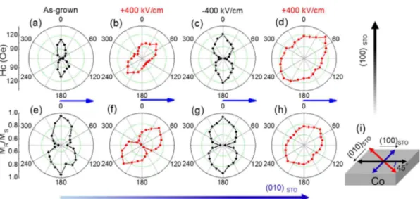
Figure 2shows the angular dependence of HCand MR/MSin the as-deposited state (a, e), after the first +400 kV/cm poling (b, f), after the subsequent −400 kV/cm (c, g), and after the second +400 kV/cm poling (d, h). ±400 kV/cm corresponds to ±3.5 V, and for each poling, the voltage is applied for approximately 10 s. The HCand the MR/MSboth reach maxima at 0° (and 180°) and minima at 90° (and 270°) in the as-grown state (a and e), indicating that the easy and the hard axes of the Co pad are along the (100) and the (010) crystallographic axes of the STO layer (i.e., 0° and 90° in the polar curves), respectively. (We note that because the (100) direction and the (010) direction here are equivalent, for a given device, we denote the initial easy axis direction as the (100) direction.) The polar curves have the typical shapes of angular dependence of the HC and the MR/MS in a conventional ferromagnet/ antiferromagnet exchange-biased system.24,25
After a positive voltage (+400 kV/cm) pulse was applied to the same pad, the HCand the MR/MSnow exhibit their maxima and minima at 45° and 135°, respectively (Figure 2b and f). The results suggest that, after the E-field poling, the easy and hard axes are now located at 45° and 135°, respectively. The easy axis now is along the (110) or (−110) directions. As shown inFigure 2c and g, after applying a −400 kV/cm E-field pulse on the same sample pad, the easy and the hard axes switch back to 0° and 90°, respectively, which are the starting crystallographic (100) and (010) directions of the STO film.
Figure 2d and h show the angular dependence of HCand MR/
MSafter the second positive E-field pulse (+400 kV/cm) was applied. The easy axis has once again rotated 45°.
The results here clearly demonstrate that the easy axis of the Co layer reversibly switches back and forth with applied polarity-alternating E-field pulses. This indicates that there is reversible change in the AFM domains of the BFO film, which determines the exchange bias and its direction in the Co layer. The AFM domains are in turn directly associated with the FE polarization of the BFO film.13
It has been explained theoretically that, in strained BFO films with stripe domains, there are G-type AFM domains with local AFM moments oriented in the (111) planes with canted moments in the (11−2) direction.2,26It is the projection of this canted moment to the surface of the film which leads to exchange bias. There have previously been numerous experimental reports on investigation of the magnetic structure of BFO films by neutron diffraction.27−30
The general consensus is that, in strained films much thinner than 500 nm, there are G-type AFM domains, while when the films get thicker, cycloids begin to appear. We note that, due to the subtle differences in film-growth conditions among different Figure 1.Typical longitudinal magnetooptical Kerr effect (LMOKE)
hysteresis loops of a Co pad in Co (5 nm)/BiFeO3 (80 nm) film
heterostructure at hard axis (red) and easy axis (black). The inset shows the device schematic for LMOKE measurements. The magnetic field is applied in the in-plane directions (red arrows) during the MOKE measurement. The typical pad size is 100 μm × 100 μm. Note: 1 mT = 10 Oe.
Nano Letters Letter
DOI:10.1021/acs.nanolett.6b05152
Nano Lett.2017, 17, 2825−2832
groups and the subsequent residual strain states of the films, the “crossover” thickness (G-type to cycloid) differs from report to report. Most recently, Bertinshaw et al. have showed that they can grow strain-relaxed BFO films down to 100 nm and have observed cycloids at this thickness.28As we discuss below, our films used in the present study (80−200 nm thick) exhibit clear stripe domains, and they thus consist of G-type AFM domains,
which are needed to give rise to the clear exchange bias in the Co film deposited above.
Even though this canted moment geometry is consistent with the observed exchange bias behavior,23 the details of the canting has never been experimentally studied. To this end, we have carried out neutron diffraction measurements in the (HHL) scattering plane in a BFO film (200 nm) on the C5 Figure 2.Polar curves of the angular-dependent magnetic coercivity and MR/MSof a Co layer pad in Co (5 nm)/BFO (80 nm) heterostructure in an
as-grown state (a, e), after the first +400 kV/cm poling (b, f), after the subsequent −400 kV/cm poling (c, g), and after the second +400 kV/cm poling (d, h). 0 and 90 deg indicate the (100) and (010) directions of STO substrate (long blue and black arrows), respectively; (i) schematic of 45° switching back and forth of the Co easy axis between (100) and (110) directions. The black and red arrows in (i) represent the easy axis directions of the Co layer in as-grown and (the initial) poled states, respectively.
Figure 3.Reciprocal space maps of a 200 nm thick BFO film measured in different scattering planes using neutron diffraction. Red lines represent the instrumental resolution.
triple axis spectrometer at Chalk River Laboratories in magnetic field at H ≈ 0 (except for a small guide field less than 3 mT).
Figure 3shows reciprocal space maps of a 200 nm thick BFO film revealed by neutron diffraction where only one reflection is present, which indicates that the magnetic structure of BFO film is G-type, rather than cycloids as seen in a previous study.27 In the previous study, the period of the cycloid was found to be longer. However, with our resolution (indicated in red on the figure), we would have still seen the peak splitting. Thus, we are confident that these films (80−200 nm thick) consist of G-type domains, rather than magnetic cycloids.
To precisely determine the direction of magnetic moments of the 200 nm thick BFO film, we turned to polarized neutron diffraction measurements in the HHL zone and measured the (0.5 0.5 0.5) and (−0.5 −0.5 −0.5) magnetic reflections. Several nuclear reflections from the substrate were measured to determine the flipping ratio and the uniformity of the spin transport, and flipping ratios of ≈15 were achieved. As there is a 3-fold axis about the (111) axis for rhombohedral systems, we expect magnetic domains to be present. Given equally populated magnetic domains such as in BFO, we are only sensitive to the magnitude of the magnetic moment and its angle with respect to the (111) axis. We are not able to determine the moment on an absolute scale due to our inability to measure nuclear reflections from the film, which will be shadowed by reflections from the substrate. From our fits, we find the angle of the magnetic moment with respect to the (111) is 83.9(23) degrees (≈ 84°) which is consistent with the magnetic easy plane suggested by Ederer et al.26In the fitting, we have corrected for nonuniform spin transport and for the finite flipping ratio. These results are presented in the
Supporting Information. We note that previous studies have
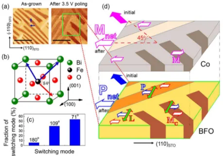
shown that the magnetic structure of these materials is very sensitive to strain, growth direction, and synthesis conditions.31 We have investigated the ferroelectric domain structures of the BFO films on STO substrates and their switching modes by piezoresponse force microscopy (PFM). The details of the PFM characterization technique is described elsewhere.13 Briefly, both out-of-plane and in-plane components of the FE polarization are simultaneously acquired from the PFM images obtained using two lock-in amplifiers.Figure 4a shows the in-plane PFM images of a 80 nm thick BFO film with the PFM cantilever oriented along the (110) direction in the as grown state and after 3.5 V poling. Here, the voltage was vertically applied between two electrodes, i.e., an SRO layer and a Pd layer (deposited above BFO for this study). To identify the polarization direction in each ferroelectric domain and their switching modes, we have taken the in-plane and the out-of-plane PFM images (not shown here) along two orthogonal (110) directions of the STO substrate. In the as-grown state, the stripe domains are clearly observed, and two colors are seen, which correspond to two possible polarization variants.31 Note thatFigure 4a only shows one of the two sets of domains in the as-grown state. The other set of domains would be appear orthogonal to the one seen here. Based on both in-plane and out-of-plane PFM images, we are able to deduce these two variants to be pointing in (−1−11) and (−111) directions. The projections of the two variants on the (001) plane marked with blue arrows in panel a. After the sample is poled at 3.5 V (400 kV/cm), the domains are now split into two sets of stripe domains orthogonal to each other: the shape/direction of some of the domains has rotated 90° with respect to the initial shape/ direction. This change is allowed because on BFO films grown on STO the two sets of orthogonal domains are equally likely. Figure 4.(a) In-plane PFM images of 80 nm thick BFO film before and after E-field poling (same area); here the PFM cantilever is pointing along (110) direction of STO substrate during PFM measurements. The images were cropped from 5 μm × 5 μm scan area images. The scale bars are 1 μm. (b) Unit cell of BFO; the blue arrows represent two FE polarization variants, and the red arrow represents the canted magnetic moments with respect to one of the polarization variants. The canted angle of the moment relative to the polarization pointing to (−111) is 84°. (c) Fractions of different switching modes observed here. (d) Schematics of magnetoelectric coupling between BFO and Co. The FE domain configuration of BFO in panel d is a representation of PFM image inside the green square in panel a. The small unfilled blue arrows represent the projections P of switched FE polarizations on the (001) plane of BFO after poling; the large solid and unfilled blue arrows represent the net polarization projections on the (001) plane Pnetbefore and after E-field poling, respectively; the unfilled red arrows represent the projection of canted moments MCafter switching;
the solid green arrows represent the antiferromagnetic axis L of BFO; the small unfilled pink arrows represent the magnetic moments of Co exchange-coupled to the projection of the canted moments in BFO after switching; the large solid and large unfilled pink arrows represent the easy axis direction of Co before and after polarization switching, respectively: the easy axis direction has switched by 45°.
Nano Letters Letter
DOI:10.1021/acs.nanolett.6b05152
Nano Lett.2017, 17, 2825−2832
Concomitantly, the domain width has also increased after E-field poling, indicating that some initial domains with different polarization directions have now merged together into a single polarization direction. Within a fixed PFM region (5 μm × 5 μm), we are able to distinguish the different switching modes (71°, 109°, and 180° switching) after E-field poling and to evaluate the switching mode fractions (Figure 4c). It can be seen that 54% and 40% of the area have undergone 71° and 109° switching, respectively, and 180° switching has taken place in less than 10% of the area. These observations are consistent with the 45° switching mechanism of the magnetic easy axis of the Co layer deposited on top of the BFO layers as discussed in the next section.
Figure 4b shows the schematic of two initial polarizations (−1−11) and (−111) directions (blue arrows). The angle between the FE polarization and the canted magnetic moment is 84° is determined by neutron diffraction, and it is shown for one of the FE polarization arrows. As discussed above, it is the projection of the canted G-type AFM moments on the (001) plane which generates the exchange bias on adjacent FM layers, and the projection direction is parallel to the projection of the polarization on the plane.Figure 4d shows the schematic of the coupling relationship between the polarization in the BFO layer and the coupled magnetic moment in the Co layer. Because we initially have equal populations of (−1−11) and (−111) domains, the net polarization projection points to the (−100) direction, as represented by the large solid blue arrow. The ferroelectric polarization and the canted moments are directly linked together with 84° via the antiferromagnetic axis L (green arrows in Figure 4d),1,2,12 and the in-plane projection of the moment is always parallel to the in-plane projection of the polarization.2The end result is that the projection of the canted AFM moments on the (001) plane initially points to the (−100) direction as an average over this region. Thus, the Co layer always has the initial easy axis in this direction (−100) represented by large solid pink arrow in the Co layer inFigure 4d. We note that we do not apply biasing magnetic field during deposition of the Co-layer on BFO and thus the easy axis direction is entirely dictated by the distribution of ferroelectric local domains in BFO. As deduced from PFM images, most of the domains undergo 71° and 109° switching (Figure 4c), and the two starting polarizations now point either both in the (−1−1−1) direction or in the (−1−1−1) and (11−1) directions after switching. Therefore, the net polarization on the (001) plane switches 45° or 135° and points to the (−1− 10) (large unfilled blue arrow) or the (110) direction. Of the two, the 135° switching is unlikely because it forms energetically unfavorable tail-to-tail domain configuration as discussed in the next section.
Because of the biaxial strain applied to BFO by STO, the other set of FE domains orthogonal to the region shown in the initial state ofFigure 4a is likely present on other parts of the same BFO film. The polarizations in these FE domains would naturally switch with the same fractional percentage modes as the polarizations shown in Figure 4a. The net polarization directions of a local region before and after E-field poling depend on which set of domains is dominant, which can vary from sample to sample and the film growth conditions,31and locally it is always 45° rotated with respect to the net polarization before poling as described above.
Let us examine the further details of the switching to see how we end up with a 45° angle but not any other angles. All possible combinations of the switching of the easy axis of the
Co layer as a result of switching of two initial polarization directions are shown in Figure 5. The red arrows depict the
average projection of the canted moments of BFO on (001) plane. Because the moments are tied to the polarizations, the in-plane directions depicted here simultaneously represent both the polarization projection and the canted-moment projection, which determines the local direction of the unidirectional exchange bias the Co layer experiences. The initial two adjacent FE polarizations of BFO point to (−1−11) and (−111) directions (Figure 4b), corresponding to coexisting variants within one set of domains, and their projections on the (001) plane of the average polarization is parallel to the net magnetic moments of the Co layer indicated by the solid pink arrow in
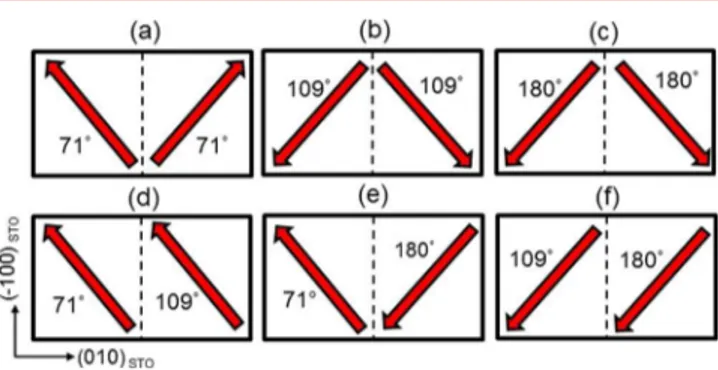
Figure 4d. After poling with a 3.5 V pulse, each polarization can undergo three possible switching: 71°, 109°, or 180°. Given the initial projection directions as shown in Figure 4b, then this results in six possible combinations of relative domain configurations for the adjacent domains after switching: namely, the two switchings are by 71°/71°, 109°/109°, 180°/180°, and 71°/109° (or equivalently 109°/71°), 71°/180° (or equiv-alently 180°/71°), and 109°/180° (or equivequiv-alently 180°/109°) where the first number is the switching angle of the left domain inFigure 5a−f and the second number after/is the switching angle of the right domain inFigure 5a−f. It has been reported that direct 180° switching in strained BFO films fabricated on STO is highly unfavorable energetically and that the two-step 180° switching is likely observed only in small-sized devices (e.g., 3 μm × 3 μm).32Thus, for our large devices (100 μm × 100 μm), we eliminate three of the six configurations which involve 180° switching inFigure 5which are panels c, e, and f. There are thus three remaining possible switching config-urations inFigure 5a, b, and d. Of the three, only the 71°/109° switching case results in a head-to-tail polarization domain boundary condition, which is energetically favorable over other configurations which result in head-to-head or tail-to-tail boundary configurations which are electrostatically unfavorable. Thus, out of all possible switching configurations, the 71°/109° case is the predominant one. This is also consistent with the fact that we observed more regions with 71° and 109° switching than ones with 180° switching (Figure 4c). As seen in
Figure 5d, this configuration leads to average direction of the projected moment at 45° from the (100) direction, resulting in exchange bias with the easy axis now rotated 45°. It is known Figure 5.Six possible switching combinations of the canted moments in the BFO layer after the first positive E-field poling. The red arrows represent the projection of moments on the (001) plane after switching. The inset numbers indicate the switching angles of polarization, which results in the corresponding moments switching, and the dashed lines are the FE domain boundary. Note that, in the cases d and f, the domains would merge to be one.
that the same but reversed path of the polarization rotation is the favorable one upon application of a reverse field.2 This results in the domains returning to the original domain configurations with the second pulse of −3.5 V, thus leading to the reversible switching of the exchange-biased easy axis of the Co-layer between (100) and (110) directions as observed here. In considering different exchange coupling mechanisms involving perovskite oxide layers, superexchange observed in heteroepiaxial superlattice structures comes to mind.33,34 In such structures, the interfacial superexchange coupling through an epitaxial interface arises from the ferromagnetic moments of the magnetic layer and the induced surface moments in the nonmagnetic layer [e.g., PrBa2Cu3O7(ref33), LaFeO3(ref34) layer)] due to the charge transfer and/or electronic orbital reconstruction at the interface. The superexchange coupling takes place only between ions (e.g., Fe3+, Mn3+, Mn4+, Cu2+, etc.) at the interface through O2−ions.
In our Co/BFO structures, we rule out the occurrence of such a superexchange mechanism. As we shown in the
Supporting Information, the Co layer is not epitaxially grown on BFO layer, and we do not expect the Co layer to be oxidized since it was deposited at room temperature. Therefore, Co2+or Co3+ cations were not provided from Co layer side for the superexchange coupling. Meanwhile, our BFO films display stripe domains, and their exchange coupling behaviors are very similar to films by Martin et al.;14 namely, we see coercivity enhancement, but there is no exchange bias shift. We therefore believe our Co/BFO coupling is similar to the exchange coupling in the CoFe/BFO interface described in Martin et al. and that the BFO moments are compensated in our samples.14 In this case, the exchange coupling in our system arises from the surface magnetic heterogeneities, such as the nanoscale domain walls.14
The difference between the deterministic 180° magnetization switching of a CoFe layer in CoFe/BFO/SRO/DSO structures previously reported by Heron et al.1,2and the 45° switching in our structures on STO is attributed to two facts. First, the different substrates give rise to different strain states imposed on BFO films, and thus there are different FE domain structures in BFO. Specifically on DSO substrates, only one set of stripe domains are observed in epitaxial BFO,1,2,35 as opposed to the two sets observed in BFO on STO. DSO has an orthorhombic structure with the lattice constant a = 5.54 Å, b = 5.71 Å, and c = 7.89 Å (pseudocubic lattice constant 3.944 Å), whereas the lattice constant of STO is a = b = c = 3.91 Å. The difference in the lattice mismatch between the substrates and BFO (a = b = 3.96 Å, c = 4.02 Å) is such that the symmetry in relative populations of different polarization domains of strained (001) BFO films grown epitaxially on DSO is broken, leading to only one set of domains in BFO on DSO.35−37
On STO, on the other hand, BFO experiences biaxial strain, resulting in roughly equal proportion of different polarization domains, giving rise to the observed PFM images with two sets of stripe domains.32,35
Second, it is known that the different device sizes and varying FE domain sizes can lead to different switching behaviors because the stability of 71°switching is associated with the domain size.32As reported in refs1 and32, the deterministic 180° switching in the 3 μm × 3 μm sized device is a two-step switching process consisting of a 71° switching and a 109° switching, where the initial 71° switched state relaxes via a subsequent 109° switching. The relaxation rate of the “intermediated” 71° switched state depends on the local FE
domain volume and is inversely proportional to the E-field poled area due to the depolarization from the unswitched area.1,32In our 45° switching case, the area size of the Co pad (E-field poled area, see the cartoon inFigure 1) is 100 × 100 or (200 × 200) μm2which is much larger than the E-field poled area in the device areas reported by Heron et al. and by Baek et al., where the 180° switching was observed.1,32
Thus, the relaxation rate from 71° switching to 180° switching in the present devices is expected to be much longer, or the relaxation rate is so long that the subsequent switching does not take place. In other words, the 71° switching is stable, and the 180° switching (71° followed by 109°) does not take place in our relatively large devices. Therefore, 45° switching of magnetization in the exchange-coupled adjacent FM layer is dominant if the BFO film is grown with biaxial strained (on STO) which results in two sets of FE domains and if the E-field is applied to a large area (≈ 100 μm2 region) in BFO film, whereas two-step 180° switching of magnetization is dominant in a smaller E-field poling area (e.g., 500 nm2region) in BFO films grown on anisotropic structural substrates such as DSO. The minimum size of the present devices (≈ 100 μm2) was limited to the size large enough for us to obtain LMOKE signals. We also note that, because of this relatively large pad size, it is possible to have both sets of domains present within a pad each exhibiting its own reversible 45° rotation locally. In such a case, depending on the relative direction of the initial polarization directions within each set of domains, the pad as a whole then might not exhibit a clear single 45 switching of the easy axis. Even in this complex scenario, we would still expect some reversible switching of the overall magnetic state to take place resulting in reversible change of the coercive field of the Co layer in some fixed directions.
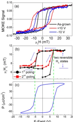
To further demonstrate the reversible control of the magnetic state of the adjacent Co-layer by E-field, we have investigated how magnetic HCchanges with the applied E-field in Co/BFO (200 nm) film heterostructure devices (100 μm × 100 μm).Figure 6a shows three representative LMOKE M(H) loops with a magnetic field applied along the (110) direction of STO substrate in the as-grown state and after applying subsequent ±10 V pulses. Clearly, the HC changes with different E-field pulses applied to the BFO layer. The HCis 4.8 mT in the as-grown state; it increases to 11 mT after a +10 V pulse poling, and then it decreases to 6.8 mT after applying the second −10 V pulse. Based on a set of M(H) loops obtained after applying different voltage pulses, we have plotted the HC of the Co layer for the initial easy axis direction as a function of the applied E-field, as shown inFigure 6b. The black curve is the HCversus E-field in the first poling cycle where the device was poled with changing amplitude of the voltage pulses from the initial state to +15 V, then to −15 V, and finally back to 0 V where each voltage pulse was applied for 10 s. In the ascending branch, the HCincreases slightly from the initial value of 4.8 mT after poling with pulses of +2 V and +5 V but rapidly jumps up to 11.0 mT at +7.5 V. The HCvalue then remains at 11.0 mT, while the amplitude of the voltage pulse further increases to as high as +15 V. In the descending branch, the HCslightly decreases from 11.0 mT at the saturation state and then jumps down to 6.8 mT after a −5 V voltage was applied. The HCvalue then remains a constant for subsequently applied pulses with increasing negative voltage amplitude. We then preformed the same measurements on the same Co pad after the first poling cycle and measured the HC as a function of E-field for the second poling cycle inFigure 6b, denoted by the red curve. The
Nano Letters Letter
DOI:10.1021/acs.nanolett.6b05152
Nano Lett.2017, 17, 2825−2832
second poling process shows two similar reversible HCstates with the first poling process: the E-field dependent HCshows a hysteresis behavior with clear two reversible HCstates (high HC and low HC).
To confirm that the observed reversible HCstates are directly correlated with ferroelectric states, we measured the polar-ization−electric field (P−E) loop of BFO film. As shown in
Figure 6c, the P−E loop of 200 nm thick BFO film shows a saturation polarization of about 70 μC/cm2 and the ferro-electric coercivity (EC) is +7.5 V and −5 V in the ascending branch and descending branch, respectively. The switching of the HC states is coincident with FE polarization switching taking place at EC, indicating that the observed two reversible
HC states are directly associated with the switching of the FE polarization of BFO.
In the present work, the mechanism of the HC-state switching is due to the reversible switching of the FE polarization in the BFO layer and the easy axis direction in the adjacent Co layer. Because the HC states are tied to the reversible modulation of the magnetic anisotropy, the effect is expected to be robust and scalable. It provides an alternative pathway of reversible magnetic state modulation compared to the 180° switching of magnetization. We have verified the reversibility of the switching in some devices with over 500 alternating voltage pulses to date. Further reversible switching cycle test is currently ongoing and will be reported in the future.
In summary, we have demonstrated reversible control of the magnetic state of a ferromagnetic Co layer by an E-field in Co/
BFO film heterostructure devices fabricated on STO substrates. The LMOKE studies on the bilayer heterostructure suggest that the easy axis of Co is reversibly switched by 45° back and forth under the voltage pulses applied on the BFO. A new switching mechanism of the net vector of the exchange coupled Co-layer coupled to the canted moment of the AFM in multidomain BFO is proposed to explain the 45° switching. These results demonstrate that the BFO devices fabricated on common STO substrates have the potential to serve as the basis for reversible
E-field switchable spin valves with low energy consumption.
The switching mechanism is a generic one since it arises naturally from the multidomain state of BFO, and reversible modulation of magnetic anisotropy provides a possible path toward device scaling. Because epitaxial STO can be prepared on Si substrates,18−20
this opens the door for fabrication of reversible multiferroic spin valves on Si.
Method.Epitaxial BFO thin films used in this study were grown under 25 mTorr oxygen environment and at 590 °C using pulsed laser deposition on (001) oriented STO substrates with a predeposited 50 nm SrRuO3(SRO) layer, which serves as the bottom electrode. A 5 nm thick Co layer is deposited above the BFO layer by e-beam deposition which is patterned into arrays of square pads of different sizes using a lift-off process. A 5 nm Pd cap layer was deposited on the top of the Co layer to prevent its oxidization. The root-mean-square (RMS) surface roughness of our 100 nm thick BFO films is typically 2 nm measured over 5 μm × 5 μm area.
■
ASSOCIATED CONTENT*
S Supporting InformationThe Supporting Information is available free of charge on the
ACS Publications website at DOI: 10.1021/acs.nano-lett.6b05152.
Details on the microstructure and on the neutron diffraction measurements (PDF)
■
AUTHOR INFORMATIONCorresponding Author
*E-mail: takeuchi@umd.edu (I.T.). Tel.: (+1)-301-405-6809. Fax: (+1)301-405-6327. ORCID Tieren Gao:0000-0003-3404-6093 Shingo Maruyama: 0000-0002-6608-2219 Huairuo Zhang: 0000-0002-1984-1200 Author Contributions
I.T. and T.R.G. conceived the experiment. T.R.G., X.H.Z., S.M., M.M., P.J.C., R.S., and A.V. made the samples and devices. X.H.Z., S.M., and A.V. did the PFM measurements. T.R.G. and J.U. did the magnetic characterizations. R.W. and Z.Y. carried out the neutron diffraction experiments. K.W., H.R.Z. and L.A.B. performed the TEM characterization. T.R.G., I.T., W.R., and R.R. wrote the manuscript. All authors discussed and commented on the manuscript.
Notes
The authors declare no competing financial interest.
■
ACKNOWLEDGMENTSThis work is supported by NIST (70NANB12H238, 70NANB15H261) and in part by C-SPIN, one of six centers of STARnet, a Semiconductor Research Corporation program, sponsored by MARCO and DARPA. We acknowledge S. Figure 6.(a) LMOKE loops of Co (5 nm)/BFO (200 nm) at
as-grown state, after +10 V and −10 V poling. The Co pad is 100 μm × 100 μm; note that the magnetic fields are applied along the initial easy axis; (b) magnetic HCas a function of E-field value applied on BFO;
(c) P−E (polarization−electric field) loop of 200 nm thick BFO film. The black and red curves in panel b represent the HCversus voltages
Bowden and D. Pierce for the MOKE measurement facility at NIST. X.H.Z. acknowledges NIST-ARRA program. H.R.Z. acknowledges support from the U.S. Department of Com-merce, National Institute of Standards and Technology under the financial assistance award 70NANB15H025.
■
REFERENCES(1) Heron, J. T.; et al. Deterministic switching of ferromagnetism at room temperature using an electric field. Nature 2014, 516, 370−375. (2) Heron, J. T.; et al. Electric-Field-Induced Magnetization Reversal in a Ferromagnet Multiferroic Heterostructure. Phys. Rev. Lett. 2011,
107, 217202.
(3) Spaldin, N. A.; Fiebig, M. The Renaissance of Magnetoelectric Multiferroics. Science 2005, 309, 391−392.
(4) Fiebig, M. Revival of the magnetoelectric effect. J. Phys. D: Appl.
Phys. 2005, 38, R123−R152.
(5) Eerenstein, W.; Mathur, N. D.; Scott, J. F. Multiferroic and magnetoelectric materials. Nature 2006, 442, 759−765.
(6) Cheong, S. W.; Mostovoy, M. Multiferroics: A magnetic twist for ferroelectricity. Nat. Mater. 2007, 6, 13−20.
(7) Chu, Y. H.; Martin, L. W.; Holcomb, M. B.; Ramesh, R. Controlling magnetism with multiferroics. Mater. Today 2007, 10, 16. (8) Balke, N.; et al. Deterministic control of ferroelastic switching in multiferroic materials. Nat. Nanotechnol. 2009, 4, 868−875.
(9) Zhang, S.; et al. Electric-field control of nonvolatile magnetization in Co40Fe40B20/ Pb(Mg1/3Nb2/3)0.7Ti0.3O3structure at room
temper-ature. Phys. Rev. Lett. 2012, 108, 137203.
(10) Wang, J.; et al. Epitaxial BiFeO3 multiferroic thin film
heterostructures. Science 2003, 299, 1719−1722.
(11) Zhao, T.; et al. Electrical control of antiferromagnetic domains in multiferroic BiFeO3films at room temperature. Nat. Mater. 2006, 5,
823−829.
(12) Chu, Y. H.; et al. Electric-field control of local ferromagnetism using a magnetoelectric multiferroic. Nat. Mater. 2008, 7, 478−482.
(13) Ratcliff, W., II; et al. Electric-field-controlled antiferromagnetic domains in epitaxial BiFeO3thin films probed by neutron diffraction.
Phys. Rev. B: Condens. Matter Mater. Phys. 2013, 87, 140405R.
(14) Martin, L. W.; et al. Nanoscale control of exchange bias with BiFeO3thin films. Nano Lett. 2008, 8, 2050−2055.
(15) Béa, H.; et al. Mechanisms of exchange bias with multiferroic BiFeO3epitaxial thin films. Phys. Rev. Lett. 2008, 100, 017204.
(16) Lebeugle, D.; et al. Exchange coupling with the multiferroic compound BiFeO3in antiferromagnetic multidomain films and
single-domain crystals. Phys. Rev. B: Condens. Matter Mater. Phys. 2010, 81, 134411.
(17) Allibe, J.; et al. Room temperature electrical manipulation of giant magnetoresistance in spin valves exchange-biased with BiFeO3.
Nano Lett. 2012, 12, 1141−1145.
(18) Kolpak, A. M.; et al. Interface-induced polarization and inhibition of ferroelectricity in epitaxial SrTiO3/Si. Phys. Rev. Lett.
2010, 105, 217601.
(19) Warusawithana, M. P.; et al. A ferroelectric oxide made directly on silicon. Science 2009, 324, 367−370.
(20) Martin, L. W.; et al. Room temperature exchange bias and spin valves based on BiFeO3/SrRuO3/SrTiO3/Si (001) heterostructures.
Appl. Phys. Lett. 2007, 91, 172513.
(21) Das, R. R.; et al. Synthesis and ferroelectric properties of epitaxial BiFeO3thin films grown by sputtering. Appl. Phys. Lett. 2006,
88, 242904.
(22) Lund, M. S.; et al. Effect of anisotropy on the critical antiferromagnet thickness in exchange-biased bilayers. Phys. Rev. B:
Condens. Matter Mater. Phys. 2002, 66, 054422.
(23) Lebeugle, D. A.; et al. Electric-field-induced spin flop in BiFeO3
single crystals at room temperature. Phys. Rev. Lett. 2009, 103, 257601. (24) Nogués, J.; Schuller, I. K. Exchange bias. J. Magn. Magn. Mater. 1999, 192, 203−232.
(25) Gao, T. R.; et al. Hysteretic behavior of angular dependence of exchange bias in FeNi/FeMn bilayers. Phys. Rev. Lett. 2007, 99, 057201.
(26) Ederer, C.; Spaldin, N. A. Weak ferromagnetism and magnetoelectric coupling in bismuth ferrite. Phys. Rev. B: Condens.
Matter Mater. Phys. 2005, 71, 060401.
(27) Ke, X.; et al. Magnetic structure of epitaxial multiferroic BiFeO3
films with engineered ferroelectric domains. Phys. Rev. B: Condens.
Matter Mater. Phys. 2010, 82, 134448.
(28) Bertinshaw, J.; et al. Direct evidence for the spin cycloid in strained nanoscale bismuth ferrite thin films. Nat. Commun. 2016, 7, 12664.
(29) Sando, D.; et al. Control of ferroelectricity and magnetism in multi-ferroic BiFeO3by epitaxial strain. Philos. Trans. R. Soc., A 2014,
372, 20120438.
(30) Ratcliff, W., II; et al. Neutron Diffraction Investigations of Magnetism in BiFeO3 Epitaxial Films. Adv. Funct. Mater. 2011, 21,
1567−1574.
(31) Chu, Y. H.; et al. Nanoscale domain control in multiferroic BiFeO3thin films. Adv. Mater. 2006, 18, 2307−2311.
(32) Baek, S. H.; et al. Ferroelastic switching for nanoscale non-volatile magnetoelectric devices. Nat. Mater. 2010, 9, 309−314.
(33) Cuellar, F. A.; et al. Reversible electric-field control of magnetization at oxide Interfaces. Nat. Commun. 2014, 5, 4215.
(34) Bruno, F. Y.; et al. Insight into spin transport in oxide heterostructures from interface resolved magnetic mapping. Nat.
Commun. 2015, 6, 6306.
(35) Chu, Y. H.; et al. Nanoscale control of domain architectures in BiFeO3thin films. Nano Lett. 2009, 9, 1726−1730.
(36) Jang, H. W.; et al. Domain engineering for enhanced ferroelectric properties of epitaxial (001) BiFeO3 thin films. Adv.
Mater. 2009, 21, 817−823.
(37) Chen, Z. H.; et al. Effect of “symmetry mismatch” on the domain structure of rhombohedral BiFeO3thin films. Appl. Phys. Lett.
2014, 104, 182908.
Nano Letters Letter
DOI:10.1021/acs.nanolett.6b05152
Nano Lett.2017, 17, 2825−2832