Anisotropic and Tunable Characteristics of the Colloidal Behavior of Metal Oxide Surfaces by
Joseph W. Bullard, III
B.S. Materials Science and Engineering (2000) Rice University
S.M. Materials Science and Engineering (2003) Massachusetts Institute of Technology
SUBMITTED TO THE DEPARTMENT OF MATERIALS SCIENCE AND ENGINEERING IN PARTIAL FULFILLMENT OF THE REQUIREMENTS FOR THE DEGREE OF
DOCTOR OF PHILOSOPHY IN MATERIALS SCIENCE AND ENGINEERING AT THE
MASSACHUSETTS INSTITUTE OF TECHNOLOGY SEPTEMBER 2006
© 2006 Massachusetts Institute of Technology. All rights reserved.
Signature of Author:
)
bepartment-ýM terials Science and Engineering June 28, 2006,K?/A
Certified by: zý///7/ 0 -v vL - I 1 "1L .---.L Michael J. Cima Sumitomo Electric Industries Professor of Engineering Thesis Supervisor4
Accepted by:
zC-(
0sc Me tallurgPOSCO Professor of Ph,
Chair, Departmental Committee on
MASSACHUSM8N E OF TECHNOLOGY
OCT
0 2 2006
LIBRARIES
Samuel M. Allen ysical Metallurgy Graduate StudiesARCHIVES
i ... / I &Anisotropic and Tunable Characteristics of the Colloidal Behavior of Metal Oxide Surfaces
by
Joseph W. Bullard, III
Submitted to the department of Materials Science and Engineering on June 28, 2006, in partial fulfillment of the requirements for the
degree of Doctor of Philosophy in Materials Science and Engineering.
ABSTRACT
The electroosmotic behavior of the rutile polymorph of titanium dioxide was explored as a function of crystallographic orientation. Atomic force microscopy (AFM) was employed to make high-resolution force spectroscopy measurements between a silica sphere attached to a traditional, contact-mode AFM cantilever and TiO2 (110), (100), and (001) surfaces in aqueous
solutions. Measurements were taken in a variety of solution conditions across a broad range of pH values, and the resultant force-distance curves were used to deduce relative behaviors of each orientation of rutile, with particular interest in changes of the isoelectric point (iep). Differences in iep as a function of orientation are explained in terms of differences in both the coordination number and density of (Lewis) acidic and basic sites on the surface. The results were supported by angle-resolved X-ray photoelectron spectroscopy (XPS) measurements of a nominal monolayer of palladium metal deposited on each of the three orientations studied. The palladium monolayer served as a means of probing the relative electron affinities of the three surfaces studied, which was exhibited in shifts of the palladium XPS peak that corresponded to differences in binding energy as a function of substrate orientation. The correlation between rutile orientation and shift in palladium binding energy corresponded directly to the relationship between isoelectric point and orientation, with the surface of lowest isoelectric point exhibiting the highest Pd binding energy.
Force spectroscopy was also used to investigate the changes in the electroosmotic behavior of rutile surfaces induced by exposure to ultraviolet irradiation (UV). Force-distance measurements using a silica sphere in aqueous potassium chloride solutions were performed on surfaces exposed to UV, and compared with data taken on identically oriented surfaces stored in darkness. Changes in the characteristics of both the extension and retraction components of the force measurements were observed. Differences in the former suggest changes in the double layer characteristics of the rutile surfaces, whereas differences in the latter denote changes in the adhesion forces between the probing silica sphere and the surface.
Thesis Supervisor: Michael J. Cima
ACKNOWLEDGEMENTS
The completion of my thesis has at times felt rushed, while at others it has seemed brilliantly stimulating. Still other occasions of reflection have crushed me with its seemingly impossible weight. Pausing for a moment to take stock in my time at MIT, I am left, after six wonderful and difficult years, with more questions to ask than ones I have answered. I remain uncertain about many things, but am absolutely sure about a single truth: I did not do this alone.
The work detailed in these pages is a testament to the power of collaboration and the fruit of the labors of many. Help has come in many forms over the past six years, and has at times come from people who were likely unaware that they were even giving it. Help has also come both directly and indirectly, as insightful analysis in the lab and as nonsensical humor at the pub, as well as in many ways between. There is no way to express how grateful I am for all of it, and I will not be able to do its impact justice in just a few short paragraphs.
I would like to begin by thanking my thesis advisor, Michael Cima. His guidance and support over the years have helped to mold this work in so many ways, and I am grateful for his mentorship. Michael's approach to materials science is nothing short of inspirational; his ability to identify important technological problems and chart an effective course of study amazes me, and his firm grasp of such a breadth of relevant fields is something to aspire to. My time in his lab has taught me far more than the work presented here, and I will constantly look to his example as I begin to develop my own scientific career.
I must also thank the numerous members of CPRL, whose input, friendships, and support have been invaluable to me on a daily basis. I would like to particularly thank Ryan Kershner, with whom I worked so closely during the first six months of my time in Michael's lab. The strides made in his thesis and the time we spent working together truly laid the foundation to the work in this thesis. I would also like to thank Chris Vassiliou and Dan Wesolowski, who at various times put their own projects aside to lend their programming expertise to me. What took them many hours may have saved me many months. I am also indebted to Barbara Layne, Lenny Rigione, and John Centorino for all of their support in so many ways over the years.
There are also a number of students and staff around MIT and outside of CPRL who have provided me with their time, talents, and insights over the years. Libby Shaw, Kurt Broderick, David Bono, Tim McLure, Jorge Feuchtwanger, Jen Vandiver, and Siddarth Kumar have all given so much to me so generously in many different ways.
I have also been fortunate to have made many great friendships in my time at MIT. Spending Wednesday evenings at the Muddy with Josh Hertz, Dan Sparacin, Ryan Williams, and Nate Vandesteeg is something that I always looked forward to, and sharing in a good laugh, a spirited debate, or musings of work-related struggles has been an invigorating source of support to me. I will take with me many memories of so many wonderful times with them at MIT.
Coming home to Boston after four years of college in Texas has also been an amazing blessing in my time at MIT. To celebrate holidays, to enjoy a dinner with my parents, wife, and sister at the house where I grew up, to spend Christmas with grandparents, aunts, uncles, and cousins, has
been a joy. I would like to particularly acknowledge my parents, Joe and Bonnie, who have always taken a loving interest in my successes and failures. Their emphasis on hard work and their enthusiasm for everything that I have attempted in life is something that I hope I can emulate one day with children of my own. I would also like to thank my sister, Christine, whose love and friendship I will always hold close.
Last, my wife Vanessa, who has never known me as anything but a graduate student, has been an incredible force behind the efforts detailed in these pages. Her love and support have not only helped me through my most difficult hours, but have also inspired me to strive to do my very best. She has been a sounding-board for frustration, a weekend and late-night lab companion, and a potent source of strength and encouragement for as long as I can remember. Her delicious cooking and tender care to all of life's details have lent an anchor of sanity to some very insane times, and I will always be thankful to her for all of it. She has been an inspiration and a rock, and in many ways I consider this thesis ours, not mine.
Old father, old artificer, stand me now and ever in good stead.
Table of Contents
1. Introduction ... ... ... 12
1.1 M otivation for this Study ... .. 12
1.2 Additional Areas of Importance ... ... 19
1.3 The Purpose of this W ork ... 19
1.4 Organization of the Thesis ... ... .. 20
1.5 References ... ... 21
2. Theoretical Background and Experimental Technique ... ... 25
2.1 Organization...25
2.2 Origins of the Electrical Double Layer: Gouy-Chapman Theory ... 25
2.2.1 The Poisson-Boltzmann Equation ... ... ... 26
2.3 Stern and Debye Layer Components of the EDL ... ... 30
2.4 The Double Layer and Forces Between Suspended Bodies... ... 31
2.4.1 Interactions Between Flat Surfaces of Identical Constant Potential ... 32
2.4.2 Interactions Between Different Surfaces of Constant Potential or Charge...37
2.4.3 The Derjaguin Approximation... ... 37
2.4.4 The Linear Superposition Approximation ... 39
2.5 Probing the Double Layer: Zeta Potential ... ... 40
2.6 Double Layer Formation on Oxide Surfaces ... 43
2.7 Force Distance Spectroscopy ... ... ... 44
2.7.1 General Overview ... .... .. . ... ... 44
2.7.2 Anatomy of a Force-distance Curve ... ... 47
2.8 X-Ray Photoelectron Specctroscopy ... ... 50
2.9 References ... ... 51
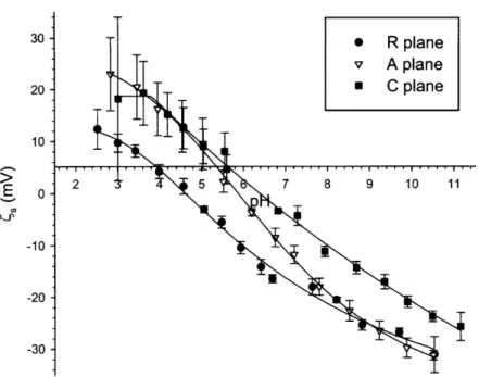
3. Orientation Dependence of Surface Properties of Sapphire ... 56
3.1 Preface ... 56
3.2 Streaming Potential and XPS Results... ... ... 56
3.3 Discussion: Developing Structure-Property Relationships ... 59
4. Anisotropy of the IEP of Rutile Surfaces ... 65
4.1 Introduction... ... 65
4.2 Materials and Methods ... 66
4.2.1 Solution and Sample Preparation... 66
4.2.2 AFM Measurements ... 67
4.2.3 Zeta Potential Measurements of Particles ... 69
4.2.4 X-ray Photoelectron Spectroscopy (XPS) ... 69
4.3 Results... ... 70
4.3.1 Zeta Potential of Silica and Rutile Powder Suspensions ... 70
4.3.2 Surface Characterization ... 72
4.3.3 Force Spectroscopy... 73
4.3.3.1 General Criterea ... 73
4.3.3.2 Correlation of AFM Data to Streaming Potential Measurements. ... 78
4.3.3.3 Force Spectroscopy Results of Rutile ... ...79
4.3.4 X-Ray Photoelectron Spectroscopy ... ... ... .. 83
4.4 Discussion...85
4.4.1 Structure of the (110) Rutile Surface...85
4.4.2 Structure of the (100) Rutile Surface ... 85
4.4.3 Structure of the (001) Rutile Surface... 87
4.4.4 Influence of Hydroxyl Groups on Surface Behavior ... 89
4.4.5 Connections Between Single Crystalline and Powder Behavior. ...,,, ... 91
4.5 C onclusions ... .. 92
4.6 References... ... 93
5. Photoinduced changes in EDL Properties of Rutile Surfaces ... 98
5.1 Introduction ... .. 98
5.2 Materials and Methods ... .. 99
5.3 Results...101
5.3.1 EDL Interactions of the Rutile (100) Surface ... 101
5.3.2 EDL Interactions of the Rutile (110) Surface ... ... 105
5.3.3 Photoinduced Changes in Adhesion Forces on Rutile Surfaces ... 108
5.4 D iscussion ... 109
5.4.1 Influence of UV on EDL Interactions ...109
5.4.2 Influence of UV on Forces of Adhesion ... 111
5.5 References ... 113
6. Summary and Future Work ... 115
Apendix: Matlab AFM Analysis Program ... ... 120
Chapter
1:
Motivation, Purpose and Organization of this Thesis
1.1
Motivation for this Study: Novel Assembly Methods for Novel Materials
The broad field of materials science is rife with examples of decreasing lengthscales in both emerging and extant materials technologies. The technological push for all things macro- to become micro-, and all things micro- to shrink to nano- is a driving force in reducing the size of nearly everything. This push is approached in a variety of ways, including the direct reduction of the active volumes of existing materials systems, as seen in the development of thin film and micro-battery technology. Other areas call for novel approaches to redesign existing concepts, a phenomenon clearly evident in the race to keep up with Moore's Law by finding new ways to shrink the lengthscales of electronic transistors beyond the limits of conventional microfabrication techniques. The development of nanoscale and molecular transistors falls into this category [1-3]. Entirely new classes of materials with new properties to exploit are also emerging, redefining existing materials technologies and creating new ones. Colloidal crystal technology is one such example of this, as their development has found applications in areas as diverse as microfiltration devices, photonic band gap and wave guiding materials [4-11], and useful tools for developing effective models for understanding the dynamics of atomic crystal systems [12].
As lengthscales decrease, however, practical issues of efficient assembly and production begin to appear. Micro- and nanoscale materials systems exhibit physical phenomena that lie at the overlapping boundaries of ballistic, electrostatic, and colloidal behaviors. Their high surface to volume ratios require the consideration of previously insignificant surface forces acting on systems, as macroscopic bodies are too large to be significantly affected by any of these types of interactions. The result is that conventional assembly techniques begin to break down, as the small size of functional components reduces the ability of gravitational forces to override these microscale phenomena. An example of this is found in the development of passive microscale electronic components, such as miniature multilayer ceramic capacitors. The small size of such components is critical to increasing their density on functional circuit boards. However, the small size is also an obstacle to the use of conventional production techniques, as electrostatic forces become too strong to "pick and place" capacitors in their desired positions in circuitry. The
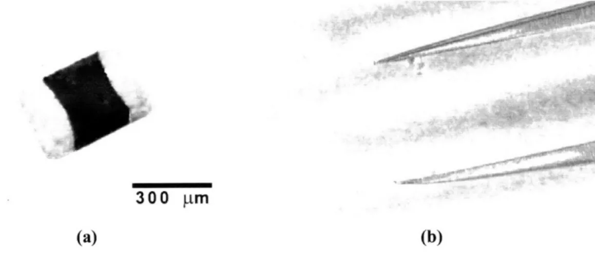
300 im
(a) (b)
Figure 1.1: (a) A photograph of of the 0201 capacitor, having dimensions on the order of 300 rim. (b) The high surface-to-volume ratio leads to the dominance of electrostatic forces over gravitational forces, and the capacitor sticks to a pair of tweezers. This illustrates the problem with using conventional "pick and place" methods in efficient assembly techniques of micro- and nanoscale electronic components. [Taken from 13]
essence of this problem is shown in Figure 1.1, where an 0201 minichip capacitor, approximately 300 p~m in length, is seen adhering to a pair of tweezers [13].
If a single capacitor is so difficult to manipulate, how can thousands be properly and efficiently positioned in their precise locations on a circuit board? Clearly, new approaches are required, and the surface forces impeding the use of conventional technologies must be at least understood, and ultimately manipulated. An example of a possible approach to a solution can be found in a proposal to integrate optoelectronic components such as GaAs LEDs on a silicon substrate [14]. The proposed approach requires the fabrication of trapezoidal LED components and etching pits of matching geometry in a silicon substrate, as shown in Figure 1.2. The devices are then suspended in a fluidic medium above the patterned substrate, and an external source of acoustic vibration is provided to hasten the settling of components into their desired locations. The directional geometry of both substrate and device allows for a lock-and-key type of fit, which enables the self-alignment of the LEDs in their positions. One significant observation from these experiments was that placement efficiency was inversely related to component size. Relatively large, 1 mm LEDs were readily positioned in their proper locations with near-perfect success. A reduction in LED size, however, corresponded to a decrease in positioning efficiency. Once again, this result can be attributed to increases in surface-to-volume ratios of the smaller devices, leading to an increase in the influence of surface forces relative to the gravitational
Tý
000,
ý__
metal contacts
Figure 1.2. Schematic diagram of a proposed sacrificial Si substrate process for the fluidic assembly of GaAs LEDs
on a patterned silica surface. The devices are fabricated to have a trapezoidal geometry (top), which promotes proper alignment between the patterned surface (bottom) and the electrical
contacts of each LED. Taken from [141. gap
forces relied on for the positioning of larger components. While the initial successes of this method are evident, its shortcomings speak to the importance of studying the origins of these
surface forces for improved assembly techniques.
Future generations of electronic devices are similarly plagued with controllable assembly issues defined by interactions between surfaces of various components. The fabrication of effective molecular transistors, for example, requires the placement of carbon nanotubes or other transistor molecules or nanoparticles between a pair of gold electrodes and above a gate dielectric [1-3], which is usually a silica or alumina surface. An example of a molecular transistor is shown in Figure 1.3. Current positioning techniques, however, involve suspending transistor molecules or nanotubes in solution and placing a droplet of the solution on top of an array of electrodes and deposited gate oxide. Successful positioning (and, consequently, transistor fabrication) relies upon achieving a desirable ratio of suspended molecules to patterned
electrode pairs, and is highly uncertain.
Regardless of the laboratory successes of nanoscale and molecular electronic devices, their transfer to the marketplace will not be possible without effective, efficient assembly methods. Separation distances between electrodes can be on the order of Inm, rendering the interactions between oxide surface and transistor molecules crucial to developing more effective
It
N~T~V-P
A
Figure 1.3. Image of an early molecular transistor. The bottom inset shows the nanoscale separation distances between source and drain, whereas the top inset shows a schematic of the cross-sectional view. The lengthscales of the entire transistor are on the order of interactions between the alumina substrate and the transisting molecule (shown above). These issues would also translate into electronic components build with small nanoparticles, as well. [Taken from 2].
placement techniques. A recent approach this problem capitalizes on the unique ability of various metal oxide surfaces to form self-assembled monolayers (SAMs) of phosponic acids, which can be tuned to selectively prevent or enhance the adsorption of single-walled carbon nanotubes [15]. However, the dimensionality of the controlled selectivity is limited by existing microcontact printing and lithographic techniques. Other researchers are attempting to use variations of conventional electrophoretic deposition processes to assemble transisting molecules at electrical contacts [16], illustrating both the richness of opportunity and the depth of difficulty in harnessing surface forces to work in favor of assembly.
The synthesis and manipulation of colloidal crystal systems is another growing area of materials technology with direct ties to studies in the surface forces that govern particle manipulation. These types of materials have found new and unique applications in a breadth of fields in recent years. Photonic bandgap materials, for example, can be produced by the arrangement of dielectric materials in periodic structures designed to filter specific electromagnetic states [4-6]. Colloidal crystals have been used to act either as a photonic material itself or as a template to be filled with a second material [4-11]. This latter technique,
upon removal of the templating microspheres, results in a porous periodic structure having a continuous air phase [8-11]. Recent work has utilized these structures as optical waveguides, with specific patterns of defects engineered into the crystal to guide light in a specified direction [17]. A variety of applications beyond photonics are also possible for these structures, including the development of microfilters and more efficient catalysts. Colloidal crystals have also found applications serving as model structures for the study of the mechanical deformation of solids at the atomic scale [12].
Colloidal crystal systems, however, are fundamentally limited by existing synthesis techniques. The predominant means of production of relatively large crystals relies on simple sedimentation processes or derivatives thereof [18-20]. This results in the close packing of each plane of particles, and the
{
111}
FCC orientation emerges as the only family of crystallographic surface terminations. Expanding the library of available crystal structures to colloid-based materials is critical to seeing its full promise reached as a new class of structures. Some methods have been already developed to create non-FCC crystals, but certain processes can be extraordinarily slow. Construction of a diamond cubic cell is possible, however, but it requires the individual positioning of colloid spheres of two different materials in alternating locations of a stack close-packed plane, followed by heat treatment above the decomposition temperature of one material and below the decomposition of the other [21], which leaves vacancies at exactly half of the lattice sites of the original structure. This method works well for constructing small structures for research purposes, but is not readily transferable to large-scale production techniques.Various thrusts of materials research are now aimed at resolving the issues of directed assembly which are problematic to these myriad micro- and nanoscale technologies. One particular area of research that pertains to the work presented here is that of template systems for the direction of particle assembly. Ideal approaches to templated assembly capitalize on the very surface forces that impede the use of conventional production techniques, as they can be designed to either attract or repel suspended particles at specific locations on the substrate surface. Several micro-contact printing methods, for example, have been utilized to create templates to dictate the ordering of colloidal crystals, providing a means of producing ordered arrays of colloids on a surface [22-25]. The production of such materials using templated
assembly techniques requires a developed understanding of the interplay between template surface structure and its environment.
The essential component of any template-based approach to the directed assembly of any type of suspended media is the local variation of surface characteristics. Put simply, an effective template will have specified areas of strongly attracting and (ideally) repulsing interactions between substrate and suspended matter. There is no reason that such heterogeneous surface structures cannot be utilized as substrates for selective adsorption and templates for the directed assembly of molecular electronics as well as nano and microscale particles; the same fundamental principles should apply at any lengthscale.
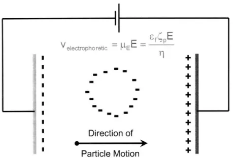
A large emphasis in this field of study is the use of organic materials as the primary means of adding functionality to a surface. Self-segregating block copolymers, for example, readily assemble into ordered surfaces with periodically varying local characteristics [26-29]. The use of tailored monomer chemistries is an effective means for careful control of specific surface properties. The potential for engineered patterns of variant surface properties of inorganic crystals is certainly extant [30-34], and some have been engineered in the form of multi-material systems with applications in colloid science in mind. Work by Aksay, for example [34], uses masked ITO substrates to define locations preferable for particle adsorption. The photoresponsive behavior of the substrate is then used to electrophoretically manipulate suspended particles into their desired location. An example of this is shown in Figure 1.4.
Figure 1.4. SEM images of the electrophoretic deposition of silica particles on an indium tin oxide (ITO) surface with specific regions of the surface exposed to light. From [34].
Such designer materials are less susceptible to degradation in numerous environments, largely insensitive to factors such as ultraviolet radiation, and stable over dramatically longer periods of time than their organic-based counterparts. Multi-material templates, however, are fundamentally limited by the limits of their processing lengthscales. Similar designer patterns on crystalline surfaces, on the other hand, might be achieved by careful control of defect structures and inclusion chemistry, reducing the complexity of the system and diminishing the roughness of the patterned surface to the order of a few angstroms. Cultivating this type of technology would rely on a well-developed understanding of relevant structure-property relations at the atomic
level in crystal systems of interest.
The importance of atomic structure to colloidal behavior is outlined in subsequent chapters of this thesis. One natural conclusion drawn from a developed understanding of the intimate relationship between structure and properties is the assumption that changes in the atomic and electronic landscape of a particular surface will result in changes in the behaviors exhibited by that surface. This leads to further possibilities for using specific oxide surfaces as assembly templates by exploiting the externally tunable behaviors exhibited in certain types of systems. Surfaces of such active materials could serve as loci of functional interactions with a colloidal system. Conditions might be varied locally, for instance, to alter the nature of interactions with suspended particles, or to control the reaction of a dissolved molecule at the interface.
A variety of metal oxide systems of varying complexity currently exist with the potential for tunable applications. These include both piezoelectric and ferroelectric materials such as quartz and strontium titanate, as well as photoresponsive materials such as the rutile and anatase forms of titanium dioxide. The well-known behavior of piezoelectric materials, for example could used to alter the electronic properties of a surface under the influence of an external mechanical stimulus. This approach is used in reverse in the field of surface acoustic wave (SAW) chemical sensors, class of devices used for, among other things, the detection of biological agents in liquid media [56-57]. Typical SAW sensors consist of a piezoelectric crystal coated with an active layer to which ambient molecules adsorb. The presence of these adsorbed species is indicated in changes in the velocity and attenuation of acoustic wave signals generated between patterned electrodes on the piezoelectric surface. Applied electric fields might be used in lieu of mechanical stimuli with ferroelectric materials to the same effect. The crystal structures
such as the strontium and barium titanates are known to contain cations that can shuttle between a pair of lattice sites depending on the direction of an applied field. This phenomenon might find relevance in template technology as the atomic structure of a surface would be altered as these cations were moved closer to or farther from the surface in an applied field.
One drawback of using piezoelectric or ferroelectric systems for the work proposed here is that in both cases, the external stimuli would affect the entire system that it interacts with. Although their intensities can vary as a function of location, mechanical stresses and electric fields cannot be readily targeted to discrete positions across the continuum of a surface. Photoresponsive materials, however, are more susceptible to highly local events, as incident irradiation can readily be masked in locations where it is not desired. This permits increased system complexity, as the impact of the external stimulus can now be varied not only temporally, but spatially as well.
1.2 Additional Areas of Importance
The governing principles that make atomistic studies of colloid behavior important in advancing directed assembly techniques also pertain to other emerging materials technologies. One example of the direct impact of studies on titania surfaces ties in with recent work by Moorthy and coworkers, who used the photoresponsive properties of TiO2 films to modulate
elecroosmotic flow in microfluidic channels [37]. The success of their work was rooted in the production of electrons at the surface of the films, whose presence altered the surface potential of the titania-coated walls of the channel. Control of flow in microfluidic channels through external means may have applications in drug delivery and discovery as well as in novel filtration techniques.
Oxide surfaces also serve as passive components in other forms of particle control. The electrophoretic manipulation of micron-sized silica particles, for example, has been studied between microelectrodes patterned onto sapphire surfaces [38-39]. Because the particles and microelectrodes are of similar lengthscales, interactions between the two essentially occur directly on the substrate surface. This was shown to be important, as Faradaic processes at both electrodes produced H+ and OH- groups which locally altered the pH, and thus the surface potential, of the sapphire substrate. The result was a significant shift from repulsive to attractive
interactions between the suspended particles and the underlying substrate, which led to the adhesion of previously mobile particles onto the sapphire surface rather than the patterned electrodes. A continued bias across electrodes resulted in further electrolysis of water, which continued to shift interactions between surface and particles from repulsive to attractive at increasing distances away from the electrodes.
1.3 The Purpose of this Work
These studies aim to establish quantitative relationships between the structure and functionality of metal oxide surfaces in aqueous media. Specifically, the work relates the electro-osmotic properties of a crystalline surface to its structure, rather than just its chemistry. This approach bridges the crystal chemistry of a surface and the specific absorption and desorption of ions in an electrolyte. Such phenomena are at the heart of the development of the technologies outlined above, and their understanding is therefore critical. Thus far, only minimal work has been done in exploring the connections between the structures of inorgainc surfaces and their aqueous chemistry behavior. Forging the links between a macroscopic property such as the isoelectric point of a material and the atomistic features of a crystal also creates closer connections between the nanoscale and the micron scale. Progress on this front in both alumina and titania oxide systems is presented, with thorough discussion of the relationship between surface structure and observed anisotropy.
The role that external stimuli can play in controlling the electro-osmotic behavior of systems is also explored. Model surfaces of single crystalline titanium dioxide are again used, with work focusing on the influence of ultraviolet irradiation (UV) on the behavior of these surfaces in solution. Capitalizing on the photoactivity of this system illustrates the viability of specifying surface functionality through external means, and may prove to be an effective approach to manipulating surfaces both spatially and temporally with applications in directed assembly, flow modulation, and flocculation control.
1.4 Organization of this Thesis
This author has attempted to organize the work detailed in these pages into a series of largely self-contained chapters, with each chapter featuring a smaller project that contributed to the whole of the thesis. The result is a document that might be regarded as a series of separate,
but interrelated academic papers. As such, each chapter contains its own discussion on the specific motivations for the work it contains, as well as its own descriptions of experimental procedure, presentation of results, and relevant discussion in terms of the larger body of academic work on the topic at hand. The most glaring of redundancies are eliminated by presenting in a single chapter both the theoretical framework of the phenomena studied here and the foundational principles of the most important experimental techniques. The thesis concludes with a chapter proposing a series of possible experiments to build on the work discussed here, and an appendix containing the major components of a Matlab analysis program written for the manipulation of AFM data.
1.4 References
[1] A. Bachtold, P. Hadley, T. Nakanishi, and C. Dekker, "Logic circuits with carbon nanotube transistors." Science 294 (2001) 1317
[2] W. Liang, M.P. Shores, M. Bockrath, J.R. Long, and H. Park, "Kondo resonance in a single-molecule transistor." Nature 417 (2002) 725
[3] A.W. Ghosh, P.S. Damle, S. Datta, and A. Nitzan, "Molecular electronics: Theory and device prospects." Mat. Res. Bull. 29 (2004) 391
[4] J.E.G.J.Wijnhoven and W.L. Vos, "Preparation of photonic crystals made by air spheres in titania." Science 281 (1998) 802
[5] A. Imhof and D.J. Pine, "Ordered macroporous materials by emulsion templating." Nature 389 (1997) 948
[6] Y.A. Vlasov, X.-Z. Bo, J.C. Sturm, and D.N. Norris, "On-chip natural assembly of silicon photonic bandgap crystals." Nature 414 (2001) 289
[7] P.V. Braun and P. Wiltzius, "Microporous materials - Electrochemically grown photonic crystals." Nature 402 (1999) 603
[8] O.D. Velev, and E.W. Kaler, "Structured porous materials via colloidal crystal templating: From inorganic oxides to metals." Adv. Mater. 12 (2000) 531
[9] D.J. Norris and Y.A. Vlasov, "Chemical approaches to three dimensional semiconductor crystals." Adv. Mater. 13 (2001) 371
[10] V.G. Solovyev, S.G. Romanov, C.M. Sotomayor Torres, M. Muller, R. Zental, N. Gaponik, A. Eychmuller, and A.L. Rogach, "Modification of the spontaneous emission of CdTe nanocrystals in TiO2 inverted opals." J. App. Phys. 94 (2003) 1205
[11] Y. Xia, B. Gates, Y. Yin, Y. Lu, "Monodispersed colloidal spheres: Old materials with new applications." Adv. Mater. 12 (2000) 693
[12] P. Schall, I. Cohen, D.A. Weitz, and F. Spaepen, "Visualization of dislocation dynamics in colloidal crystals." Science 305 (2004) 1944
[13] M.M. Tupper, Fabrication and Assembly of Micron-Scale Ceramic Components, Doctoral
Thesis, M.I.T., 2004
[14] H.J. Yeh and J.S. Smith, "Fluidic self-assembly for the integration of GaAs light-emitting diodes on Si substrates." IEEE Photo Tech Lett 6 (1994) 706
[15] J.B. Hannon, A. Afzali, Ch. Klinke, and Ph. Avouris, "Selective placement of carbon nanotubes on metal-oxide surfaces." Langmuir 21 (2005) 8569
[16] T. Teranishi, "Fabrication and electronic properties of gold nanoparticle superlattices."
Comptes Rendus Chimi 6 (2003) 979
[17] M. Piech, M.C. George, N.S. Bell, and P.V. Braun, "Patterned colloid assembly by grafted photochromic polymer layers." Langmuir 22 (2006) 1379
[18] S. Noda, K. Tomoda, N. Yamamoto, and A. Chutinan, "Full three-dimensional photonic bandgap crystals at near-infrared wavelengths." Science 289 (2000) 604
[19] W. Lee, A. Chan, M.A. Bevan, J.A. Lewis, and P.V. Braun, "Nanoparticle-mediated epitaxial assembly of colloidal crystals on patterned substrates." Langmuir 20 (2004) 5262 [20] J.P. Hoogenboom, D. Derks, P. Vergeer, and A. van Blaaderen, "Stacking faults in colloidal
crystals grown by sedimentation." J Chem Phys 117 (2002) 11320
[21] F. Garcia-Santamaria, H.T. Miyazaki, A. Urquia, M. Ibisate, M. Belmonte, N. Shinya, F. Meseguer, and C. Lopez, "Nanorobotic manipulation of microspheres for on-chip diamond architectures." Advanced Materials 14 (2002) 1144
[22] A. Kumar, H.A. Biebuyck, and G.M. Whitesides, "Patterning self-assembled monolayers: Applications in materials science." Langmuir 10 (1994) 1498
[23] J.L. Wilbur, A. Kumar, H.A. Biebuyck, E. Kim, E., and G.M. Whitesides, "Microcontact printing of self-assembled monolayers: Applications in microfabrication." Nanotechnology 7 (1996) 452
[24] P. Yang, T. Deng, D. Zhao, P. Feng, D. Pine, B.F. Chmelka, G.M. Whitesides, and G.D. Stucky, "Hierarchically ordered oxides." Science 282 (1998) 2244
[25] K.M. Chen, X. Jiang, L.C. Kimerling, and P.T. Hammond, "Selective self-organization of colloids on patterned polyelectrolyte templates." Langmuir 16 7825 (2000) 7825
[26] I.W. Hamley, "Nanostructure fabrication using block copolymers." Nanotechnology 14 (2003) R39
[27] M.F. Rubner in Multilaver Thin Films, Eds. G. Decher and J.B. Schlenoff (Wiley, Weinheim, 2003) 133-154
[28] X. Jiang, H. Zheng, S. Gourdin, and P. Hammond, "Polymer-on-polymer stamping: Universal approaches to chemically patterned surfaces." Langmuir 18 (2002) 2607 [29] M. Husemann, M. Morrison, D. Benoit, J. Frommer, C.M. Mate, W.D. Hinsberg, J.L.
Hendrick, and C.J. Hawker, "Manipulation of surface properties by patterning of covalently bound polymer brushes." J. Am. Chem. Soc. 122 (2000) 1844
[30] C.L. Brown, I.A. Aksay, D.A. Saville, M.H. Hecht, "Template-directed assembly of a de novo designed protein." J. Am. Chem. Soc. 124 (2002) 6846
[31] M. Trau, N. Yao, E. Kim, Y. Xia, G.M. Whitesides, I.A. Aksay, "Microscopic patterning of oriented mesoscopic silica through guided growth." Nature 390 (1997) 674
[32] M. Ogawa, "Nanoporous silica films containing aluminum and titanium." Colloid Polym.
Sci. 281 (2003) 665
[33] M. Heule, S. Vuillemin, L.J. Gauckler, "Powder-based ceramic meso- and microscale fabrication processes." Adv. Mater. 15 (2003) 1237
[34] R.C. Hayward, D.A. Saville, and I.A. Aksay, "Electrophoretic assembly of colloidal crystals with optically tunable micropatterns." Nature 404 (2000) 56
[35] E. Gizeli, M. Liley, C.R. Lowe, and H. Vogel, "Antibody binding to a functionalized supported lipid layer: A direct acoustic immunosensor." Anal. Chem. 63 (1997) 4808 [36] K. Lange, F. Bender, A. Voigt, H. Gao, and M. Rapp, "A surface acoustic wave biosensor
[37] J. Moorthy, C. Khoury, J.S. Moore and D.J. Beebe, "Active control of electroosmotic flow in microchannels using light." Sensors Actuators B 75 (2001) 223
[38] R.J. Kershner, J.W. Bullard, and M.J. Cima, "The role of electrochemical reactions during electrophoretic particle deposition." J Colloid InterfSci 278 (2004) 146
[39] J.W. Bullard, R.J. Kershner, and M.J. Cima, "Scanning Probe Characterization of Localized pH Changes on a Sapphire Surface in the Presence of an Applied Field." Proc Mat Res Soc 782 (2003) A3.1.1
Chapter 2: Theoretical Background and Experimental Technique
2.1 Organization
This chapter of this thesis is intended to provide a theoretical framework within which subsequent experimental results are viewed and discussed. It provides a brief summary of the major elements of colloid science most germane to the work at hand, often referred to as DLVO theory, and begins with a discussion of the behavior of a generic dielectric surface in an electrolytic medium. This background is then focused on the specifics of behavior of metal oxide surfaces in aqueous salt solutions, and expanded to detail the models of interaction between two such interfaces in close proximity to each other.
The latter half of the chapter is dedicated to various means of quantifying the colloidal behavior of oxide surfaces, covering techniques for investigating both dispersed ceramic powders as well as flat substrates. Particular attention is paid to the methodology of making force spectroscopy measurements on a conventional atomic force microscope (AFM), as this technique serves as the primary investigative tool in the work on rutile surfaces detailed in ensuing chapters. A brief discussion of x-ray photoelectron spectroscopy (XPS) and Auger electron spectroscopy (AES) is also offered. These spectroscopic techniques were used as a secondary means of surface characterization, the results of which were correlated to direct measurements of the colloidal behavior of the oxide surfaces studied here.
2.2 Origins of the Electrical Double Layer: Gouy-Chapman Theory
Interactions between dielectric materials and aqueous solutions have long been known to result in the formation of a layer of electrical charge associated with the oxide surface, commonly referred to as the electrical double layer (EDL). EDL formation is the result of the attraction of solvated ions to the charged surface of the dielectric, which creates a localized imbalance of charge that trends towards the equilibrium condition at increased distance away from the surface (Figure 2.1). The double layer of charge necessarily results in some potential ' that is a function of the concentration of adsorbed species, which is described by a gradient away from the surface. Y(x), by definition has the boundary conditions of W(x) = To at x=O and T(x) = 0 at an infinite distance away from the surface [1-3].
2.2.1
The Poisson-Boltzmann Equation
The resultant imbalance of charge that defines EDL formation can be described as a function of the energy required to add an additional counterion, or solvated ion opposite in charge to that of the dielectric surface, from the solution to a given position away from the dielectric surface in the classic Boltzmann form:
n(x) = ex -AG) (2.1)
no
kbT
where n(x) is the concentration of counterions at some distance x away from the interface, no is the concentration of the same ion in bulk solution, and AG is the energy required to place an ion from the bulk solution to its new position at x. By definition of AG, the energy of the system is reduced by a redistribution of counterions if the work required to place a cation or anion at a given position is negative. It follows from equation 2.1 that when AG < 0 for a particular ion at a particular position, the concentration of that ion at that position will be greater than its concentration in bulk solution, and vice versa. The energy required to move an ion to a given location can be defined as
AG(x) = ze'T(x) (2.2)
where z is the valence number of the ion, e is the charge of an electron, and TP is the electrical potential. The concentration of cations and anions at a given position can then be described by the expressions:
n+ - ze~ (x) n - (-z)eP(x) (2.3)
-= exp
k
'
and - = ex
no
kbT
no kbT)
where the terms n+ and n_ denote the concentrations of cations and anions, respectively.
These Boltzmann energetics can be combined with Poisson's equation by first defining the charge density at some position away from the surface of interest as the product of the net ionic charge at that position, the valence of the ions, and the charge of an electron:
This definition of p reveals the requirement in this derivation that the valence z is the same for both cationic and anionic species.
The one-dimensional Poisson equation states that the second spatial derivative of a potential is linearly related to the volume density of charge and the dielectric constant of the medium of interest, F:
_a2 __p (2.5)
aX2
Because p is itself a function of Y(x) through equations 2.3 and 2.4, equations 2.4 and 2.5 can be combined as a differential equation known as the Poisson-Boltzmann equation. Replacing the terms n+ and n_ with the exponentials from equation 2.4 and taking the second derivative with respect to position yields the relation
a
2 2zeno ze(x) (2.6)z - 1sinh Z
ax2 E kbT
)
commonly referred to as the nonlinear Poisson-Boltzmann equation. The physical construct of such a system requires that at the surface of the material of interest, the potential must be equal to the surface potential, To, and that at infinite distance away from the surface (i.e., into the bulk
solution, the potential must be zero. These boundary conditions yield the exact solution
T+(x) =2kbT ln(+7 exp[]) (2.7)
ze
y1-
exp[nC]C
where y and K are defined as
exze(2.8, 2.9)
kbT 2e-n1
z2
exp
ze o
, 1 kbT(kkbT
This cumbersome equation is greatly simplified by using the convention that for small values of some variable t, sinh(t) is approximated as t. Therefore, for the condition that zeT(x) << kbT,
a
2T 2zen (ze(x) 2e2 z2 (x) (2.10)-ze- I I(x).
ax
26
Tkb
The definition ofK simplifies this relation further to
a2I K= .(X), (2.11)
Ox2
which has the solution
Y(x) = To exp(- Ai). (2.12)
This relationship is known to as the linear Poisson-Boltzmann equation, and shows the exponential nature of the decay of an electrostatic potential away from a dielectric surface in solution.
The Poisson-Boltzmann treatment of the EDL can also be used to describe the concentration of surface charge in terms of electrical potential. Recalling equation 2.5, the surface charge density, ao, can be related to the charge everywhere else in the liquid (i.e., far away from the interface, by charge balance. The result is that ao is defined as the negative of the integral of the solution charge density as a function of distance away from the surface:
= -p(2.13)
Oro - fpdx
x=O
Replacing p using the Poission equation, this integral becomes
0
=
2_ao
T
(2.14)
x=O
O-xx=
x
x=O
The first term of the solution approaches zero at infinite distance away from the interface (bulk conditions are met), leaving only the second term to define the surface charge density. The relationship between surface potential and distance from the interface (equation 2.12) can be
used to solve the spatial derivative on the right hand side of equation 2.14, yielding the relation
or - (2.15)
-U
/K:
1/
.. v(x) -
X,
°Oo
)exp(-Kx)
Increasing Distance from surface
-Figure 2.1. Top: Schematic diagram of the formation of an electrical double layer on surfaces of positive (red circles, left-hand side) and negative (blue circles, right-hand side) charge. Ions of charge opposite in sign to that of the surface are tightly bound in the narrow Stern layer, while a more loosely bound layer of charge is shown in the distance of one Debye length away. Bottom: The drop in surface potential is shown as a function of distance away from the surface of the dielectric interface. Potential decreases linearly across the Stem layer as it would in a generic capacitor; the decay through the Debye layer and into the bulk solution, however, follows the behavior described by the Poisson-Botlzmann equation.
C 0
CL
e .
o .
~F~PI
~
BQ
8
The second formulation of this relationship shows that as K increases with ionic strength, the
amount of charge stored in the EDL per unit potential must also increase, as the dielectric constant of aqueous solutions has been shown to retain its bulk value even in nanometer thick films [4]. Equation 2.15 does not indicate, however, whether surface charge density increases or surface potential decreases, and different systems are known to behave in different ways.
2.3 Stern and Debye Layer Components of the EDL
The Poisson-Boltzmann equation predicts an exponential decay of surface potential as a function of increasing distance away from the dielectric interface, but makes no distinction between ions positioned immediately at the dielectric interface and those slightly farther away, but still close enough to represent deviation from bulk solution conditions. The Poisson-Boltzmann derivation, as shown, considers only electrostatic interactions between the dielectric surface and the electrolytic solution. It ignores any contribution to the energetics of the system associated with the direct adsorption of solvated ions to the surface. Ions that interact with the surface in this manner are known to be bound more tightly at the interface in comparison with ions whose presence is dictated only by the electrostatic model outlined above. As a result, the EDL model must be modified to incorporate this tightly-bound layer of adsorbed counterions, commonly referred to as the Stern layer.
The addition of the Stem layer to the Gouy-Chapman model of the EDL results in the delineation of two distinct components of the EDL: The relatively narrow region of tightly-bound, oppositely-charged counterions in the Stern layer, and the region of charge whose potential and concentration are dictated principally by electrostatic interactions, referred to as the diffuse or Debye layer. The thickness of the Stem layer remains essentially constant for a given system of surface material and solution chemistry, as it is defined as a layer of counterions tightly bound to the dielectric surface. Typical thicknesses of the Stern layer are therefore on the order of the radii of adsorbing species, or 1-3 A. The Debye layer, on the other hand, is a function of the ionic strength of the solution, and is defined by its inverse as:
e' n2z, (2.16)
KC= i
A comparison of 2.9 to 2.13 shows that the above definition of the inverse of the Debye layer is only a more generalized form of the constant K used to simplify the description of the nonlinear Poisson-Boltzmann equation, which assumed a single pair of ionic species of identical valence.
The differences in the characteristics of the Stern and Debye layers is evident in the plot of surface potential as a function of distance from the surface shown in the bottom portion of Figure 2.1. The tightly-bound Stern layer is shown to influence surface potential only over a distance on the order of the lengthscale of the ionic radii of adsorbing species, but the potential drop across this layer is rapid and linear. The diffuse portion of the EDL, on the other hand, obeys the Poission-Boltzmann relation, with an exponential decay in surface potential away from the surface. With no well-defined boundary to this layer, the Debye layer provides a
characteristic length to define the limits of the EDL.
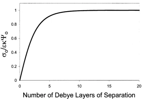
For a 1 mM solution where the valences of cationic and anionic species are equal, the Debye length 1/K is approximately 10 nm. It is worth noting that solutions ranging in concentration from 0.1 mM to 100 mM result in values of 1/K On the nanometer lengthscale, allowing for the approximation of microscale particles as flat plates. Moreover, the size of the Debye layer provides information about the lengthscales over which dielectric surfaces will interact in their suspending media, because they provide a benchmark for the distance over which the surface potential deviates strongly enough from bulk to interact with other surfaces with any significant force. Typically, the surface potential approaches zero three to five Debye lengths away from the surface of interest, a rule of thumb that will be more evident after the derivation followed in section 2.4.1.
2.4 The Double Layer and Forces Between Suspended Bodies
The introduction of one colloidal surface into the vicinity of another results in the interaction between the EDLs of the two surfaces. This leads to an exertion of electrostatic forces of each body on the other, the intensities of which are magnified as separation distances between the two bodies decreases. Interactions between such surfaces are most commonly treated in terms of overlapping surface potentials, with forces between them taken by differentiating those expressions.
Derivations of interactions between EDLs fall into four fundamental categories: Interactions between identical surfaces of constant potential, identical surfaces of constant charge,
dissimilar surfaces of constant potential, and dissimilar surfaces of constant charge. Fundamental assumptions for the derivation of the interaction between two identical surfaces of constant potential will be reviewed here as a means of exploring various events important in the interactions between the surfaces of two suspended bodies; the treatment in these pages is based largely on refs [1-2]. The results of more complex conditions are given, but not derived.
2.4.1
Interactions Between
Identical
Flat Surfaces of Constant Potential
An understanding of the forces arising from the interactions between the EDLs of separate surfaces can be viewed in terms of changes in the free energies of the EDLs from when the two surfaces are far apart to when they are in close proximity to each other. The free energyf of a single, non-interacting EDL can be shown by relating the chemical energy of an adsorbing species to the chemical energy of the same species in bulk solution as:
1 (2.17)
f= --2U o
Consider a pair of flat, identical surfaces of constant potential separated by a distance L, with the parameter x defined such that x = 0 at the midway point between the two surfaces. Because both surfaces are identical, we have the boundary condition that the potential at both x = +L/2 and x = -L/2 - that is, at the two surfaces of interest - will be the same, and will be defined as ,o.
Because the system is symmetric, changes in the potential as a function of x will be symmetric around the midway point. Therefore, - = 0 at x = 0. Using the linearized Poisson-Boltzmann
ax
equation, the relation is solved by multiplying both sides of equation 2.11 by the term 2 a which by identity ultimately yields the relation:
d
raT2 =
2c2
,T
(2.18)
dx
L
ax )8
axBoth sides of eq. 2.18 are integrated, and multiplying by -s/2 and subtracting the x-dependent right hand integrand from the left hand integrand yields results in the equation
S 2 2 - 2
=P
(2.19)2 '2 ( a Px
where the term Pm emerges from an integration constant after 2.18. Pm is dependant only on the separation distance L, and at x = 0, where it has been established that the spatial derivative of the potential is zero,
2 (atx0) (2.20)
-
ic
2
2C= P. (at
x = 0).
This definition of Pm gives way to the relation2 2
a')
2 2 2 (2.21)T2 T
2 2 ( ax 2 m
where T.m is defined as the potential midway between the two planes. The dependence of 'Pm
solely on L can be shown by rewriting equation 2.21 to define the spatial derivative of Y in terms of the square root of the difference between T2 and y'm2, and the introduction of a value 0o defined as the inverse hyperbolic cosine of TY/'Pm. It should be noted that the spatial derivative of T can now be defined as Ymsinh(o). It can be shown from these relationships and a few
substitutions that
do
= /cosh2
-- 1 (2.22)dx
The identity Vcosh2 wo-1 is also sinh(o), and therefore the spatial derivative of o0 is shown to be equal to the Debye layer, K. Integrating to solve for o can be achieved by remembering the boundary condition that at x = +L/2, o becomes the hyperbolic cosine of TYo/m. This is
important in determining the integration constant, which allows for the definition of o in other terms:
(O=KCX L) >cosh-' Tj (2.23)
Remembering the original definition of w in terms of T(x) and 'm yields an expression for '(x)
which can be defined in terms of Ym, To, K, x, and L. 'm, in turn, can be determined by setting x to 0, which results in the relation
Tm 1 (2.24)
TO coshQ"j
0.8 S0.6 E E 0.4 0.2 0 0 5 10 15
Number of Debye Layers of Separation
Figure 2.2. A plot of the midplane potential, Tm, as a function of plate separation, defined in terms of number of Debye layers, as described by equation 2.24. The relation holds only for the special case of infinitely large surfaces of constant potential (To), but shows the dramatic decline in Tm as a function of separation distance.
The relationship between mid-plane potential and plate separation is shown graphically in Figure 2.2. It is evident that TPm drops significantly after only four or five Debye layers of separation, and vanishes almost completely at distances of approximately ten Debye lengths.
The surface charge density, ,o, can be determined as it was before, defining it as the negative of the integral of the volume density of all charges in bulk solution. Symmetry arguments for the special case derived here require only the integration x between the mid-plane and one surface. The result is identical to Eq 2.14, with the only difference being the limits of integration. This relation can be combined with a relationship implicit from equation 2.21 to show the relationship between surface charge density and mid-plane potential:
2 (2.25)
U'o = 1 K )
where the relationship between mid-plane and surface potentials is shown in equation 2.24. The relationship shown in equation 2.25 is displayed graphically in Figure 2.2. One implication of
0.8 o 0.6 o 0.4 0.2 0 0 5 10 15 20
Number of Debye Layers of Separation
Figure 2.3. A plot of surface charge as a function of the separation distance between two flat, infinite plates of constant surface potential. The sharp decline of surface charge at very small separation distances is required for surfaces to maintain their potential at close proximity.
equation 2.25 is that as plate separations decrease, the charge present on both surfaces approaches zero. This result makes sense in the context of surfaces of constant potential, as a given potential can only be maintained between two plates as their separation is varied if density of charge is altered. One corollary to this observation is that for a real surface to closely approximate the behavior of an idealized surface of constant potential, its surface charges must exhibit a relatively high degree of mobility.
Using these relations, the Gibbs free energy of a pair of charged plates can be derived, which in turn provides an expression for the separation potential, VR, of two surfaces of constant potential. Having defined the free energy of an individual, charged dielectric surface in equation 2.17, the free energy of two plates of interest will be twice that value at infinite separation. Consider now the energy required to move two such plates to some separation L, attributing the change in energy to the discharge of the EDL of the two plates and assuming the surface potential to be constant:
DG is always positive, because, as seen in Figure 2.3, the surface charge density at some small separation distance L is always smaller than the surface charge density at infinite separation. This relationship can be recast in terms of surface and mid-plane potentials, expressed as
AG
=
•Yo(•
o
_ c
-T2
-
2.
(2.27)
This energy is frequently described as the reduced separation potential, VR, and equation 2.27 can be used to express VR as a function of separation distance:
6 I 1- tanh (2.28)
eXT02
2
The behavior of equation 2.28 is shown in Figure 2.4. Note that for surfaces of constant potential, there still exists a finite value of VR at L = 0, indicating that there is a finite amount of energy required to bring a pair of plates into contact with each other. Moreover, the reduced potential essentially vanishes at separation distances on the order of five Debye layers. This suggests a practical limit of the lengthscale over which interactions between suspended bodies can be expected to occur, which is determined by the solution characteristics that define the characteristic Debye length.
1 0.8 o 0.6 S0.4 0.2 0 0 5 10 15 20
Number of Debye Layers of Separation
Figure 2.4. Normalized plot of reduced potential VR, as a function of separation distance between two flat surfaces of constant TFo. VR is shown to reach a finite value at zero separation distance, as well as a near-zero value at separation distances on the order of five Debye lengths.
2.4.2
Interactions Between Different Surfaces of Constant Potential or Charge
As mentioned before, the interaction potentials of more complex systems have also been derived. Their development remains rooted in the Poisson-Boltzmann description of EDL formation and is based on considerations of the energetics and boundary conditions akin to those involved in the preceding work. A most general description of interaction energy is provided in
[5], which combines derivations of others [6-8] to describe interaction potential as
VR
-222
Y2
(2.29)
V) = T(1 - coth h)( Ti-2 - )+ sinh h
where the negative sign preceding the coth term pertains to two surfaces of constant charge and the positive sign corresponds to two surfaces of constant potential. It should be made clear that in equation 2.29, the T terms denote the potential To at the surface for two different materials, indicated by the subscripts 1 and 2, and are not dependent upon x. It can be further shown from this generic equation that for small separations, systems modeled as having surfaces of constant
charge exhibit infinite repulsion, whereas those of constant potential are shown to attract.
2.4.3 The Derjaguin Approximation
The preceding derivation for the interaction parameters of two plates demonstrates the general approach of considering such behavior, but it is limited in the fact that it was developed for the special case of two flat plates. Real systems frequently involve the interaction of suspended particles which are commonly spherical in nature. Modeling the interactions between two such spheres or between a single sphere and a flat plate is critical to understanding the dynamics of actual suspensions. Defining the forces of interaction between spheres or spheres and plates is achieved by way of a method first developed by Derjaguin [9]. Rather than calculate separation distance between spherical surfaces as continuous function accounting for the curvature of the surfaces, Derjaguin showed that any surface with a radius significantly larger than its characteristic Debye length could instead be described as a stack of flat plates of changing cross-sectional area. The energy of interaction U between two surfaces of arbitrary shape separated by some distance D could therefore be related to the energy per unit area UA of two flat surfaces separated by some distance x. This is shown schematically in Figure 2.5, as well as mathematically in the form