Publisher’s version / Version de l'éditeur:
Vous avez des questions? Nous pouvons vous aider. Pour communiquer directement avec un auteur, consultez la première page de la revue dans laquelle son article a été publié afin de trouver ses coordonnées. Si vous n’arrivez pas à les repérer, communiquez avec nous à [email protected].
Questions? Contact the NRC Publications Archive team at
[email protected]. If you wish to email the authors directly, please see the first page of the publication for their contact information.
https://publications-cnrc.canada.ca/fra/droits
L’accès à ce site Web et l’utilisation de son contenu sont assujettis aux conditions présentées dans le site LISEZ CES CONDITIONS ATTENTIVEMENT AVANT D’UTILISER CE SITE WEB.
Optics Express, 26, 22, 2018-10-19
READ THESE TERMS AND CONDITIONS CAREFULLY BEFORE USING THIS WEBSITE.
https://nrc-publications.canada.ca/eng/copyright
NRC Publications Archive Record / Notice des Archives des publications du CNRC :
https://nrc-publications.canada.ca/eng/view/object/?id=a2ab94cc-0ed4-42a8-aad1-811ec68aa918 https://publications-cnrc.canada.ca/fra/voir/objet/?id=a2ab94cc-0ed4-42a8-aad1-811ec68aa918
This publication could be one of several versions: author’s original, accepted manuscript or the publisher’s version. / La version de cette publication peut être l’une des suivantes : la version prépublication de l’auteur, la version acceptée du manuscrit ou la version de l’éditeur.
For the publisher’s version, please access the DOI link below./ Pour consulter la version de l’éditeur, utilisez le lien DOI ci-dessous.
https://doi.org/10.1364/OE.26.028651
Access and use of this website and the material on it are subject to the Terms and Conditions set forth at
Athermal echelle grating filter in silicon-on-insulator using a
temperature-synchronized input
Melati, Daniele; Verly, Pierre G.; Delâge, André; Cheben, Pavel; Schmid,
Jens H.; Janz, Siegfried; Xu, Dan-Xia
Athermal echelle grating filter in
silicon-on-insulator using a
temperature-synchronized input
D
ANIELEM
ELATI,
*P
IERREG. V
ERLY, A
NDRÉD
ELÂGE, P
AVELC
HEBEN, J
ENSH. S
CHMID, S
IEGFRIEDJ
ANZ,
ANDD
AN-X
IAX
U National Research Council Canada, 1200 Montreal Rd., Ottawa, ON K1A 0R6, CanadaAbstract: Athermal design of integrated photonic devices can reduce the need for active temperature stabilization and consequently the energy required to operate photonic integrated circuits. For silicon photonic filters such as AWGs which employ wire or ridge waveguides, temperature insensitivity can be achieved using cladding materials with negative thermo-optic coefficients. On the other hand, in echelle grating filters the inteference takes place in the slab free-propagation region, and therefore the modal overlap with the cladding is small, rendering this method ineffective. In this work we present an approach to design an athermal echelle grating filter exploiting a temperature-synchronized Mach-Zehnder interferometer as input. This reduces the spectral shift over a temperature range of 20 K to less than ±45 pm compared to the 1.6 nm shift for the same echelle grating with a conventional waveguide input. Furthermore, the proposed design relies exclusively on a standard fabrication process for silicon-on-insulator photonic devices and exhibits a good tolerance to fabrication uncertainties.
1. Introduction
The temperature-dependent behavior of integrated photonic devices is a fundamental issue that affects almost every aspect of circuit and device design and every technological platform. This is particularly true for silicon-on-insulator (SOI) and other semiconductor-based waveguides that exhibit thermo-optic coefficients almost ten times larger than that in silica. This results in large wavelength shifts of the order of several tens of picometers per degree in the optical communication bands and causes severe distortions of the device responses [1, 2]. In order to avoid or limit the use of energy-hungry active temperature control, several solutions have been proposed in the literature to mitigate the effect of temperature fluctuations by designing athermal devices. For wavelength filtering and routing, arrayed waveguide grating (AWG), lattice filter and echelle grating are the main device options, each with its advantages and shortcomings [3–6]. For AWGs and lattice filters in which the phase accumulation takes place in wire or ridge waveguides, athermal behavior may be achieved by using a material with a negative thermo-optic coefficient as the waveguide top cladding to counterbalance the positive coefficient of the core and substrates. Exploited materials include resins [7], sol-gel materials [8], polymers [9, 10], and amorphous titanium dioxide [11]. In echelle gratings where the phase accumalation is in the slab free-propagation region, a similair method has been applied to devices based on III-V semiconductors [12]. However, this method is ineffective in echelles based on a submicron silicon platform particularly for devices operating in the transverse electric (TE) polarization since the modal overlap with the cladding material is very small. Additionally, the use of these materials requires a substantial change to the standard SOI photonics fabrication processes, which may hinder their adoption outside of research scenarios. On the other hand, it is possible to utilize the dimensional dependece of the waveguide temperature sensitivity to engineer the overall device thermo-optic behavior [13, 14], and an athermal lattice filter has been reported exploiting this technique [15].
In this work we propose a way to design a SOI athermal echelle grating filter operating in the
#340356 Journal © 2018
https://doi.org/10.1364/OE.26.028651 Received 23 Jul 2018; revised 12 Sep 2018; accepted 13 Sep 2018; published 19 Oct 2018
TE polarization. We achieved the desired goal without using materials with negative thermo-optic coefficient and relying exclusively on a standard fabrication process for SOI waveguides. Inspired by the concept of wavelength-synchronized interferometers for flat-top transmission [16, 17], we exploit a temperature-synchronized (T-synced) Mach-Zehnder interferometer (MZI) as input to the echelle to match and compensate its focal position shift with temperature, thereby achieving a large reduction in the temperature dependence of the overall transmission spectrum. Unlike for the case of wavelength-synchronized interferometers, the proposed MZI is designed to have a very broad free-spectral-range (FSR) to obtain a T-synced input that has a neglegible variation with wavelength of the generated field profiles. This modified input is similar to that proposed by Kamei et al. [18] but there it was only used to compensate for the small second-order temperature dependence of silica-based AWGs in combination with resin-filled grooves. To the best of our knowledge, this is the first proposal of an athermal echelle grating in TE for the high-index-contrast SOI platform. The designed device shows a residual zero-mean wavelength fluctuation of the output spectrum and a maximum shift of less than 45 pm over a temperature range of 20 K, compared to a 1.6-nm shift for the same grating with a conventional waveguide input. The increase of the channel insertion loss due to the use of the T-synced input is limited to about 0.5 dB. Moreover, the proposed design shows a good tolerance to fabrication uncertainties, with limited degradation of the performance for waveguide width uncertainty of ±10nm.
Design concepts for the Mach-Zehnder interferometer and the interface with the echelle filter are presented in sections 2.1 and 2.2, respectively. Section 3 shows the results of the overall device simulations, the analysis of the performance and sensitivity to uncertainties.
2. Principle and design of the device
In an echelle grating filter, the incoming and outgoing angle of the light beams ϑ and ϕk are
governed by the following relation [19]:
Λ(sin ϑ + sin ϕk) = m
λk
neff(λk). (1) Here m is the order of the grating, Λ its pitch, λk the wavelength of the k-th output channel,
and neff(λk) the corresponding effective index of the slab waveguide. Since neff varies with
temperature T (i.e. thermal dispersion), the diffraction angle ϕkfor a given wavelength shifts with
T causing a shift of the focal position on the echelle image plane and hence of the transmission in the output waveguides. For an optical field distribution at the entrance of the slab that is almost insensitive to T and λ (e.g. when a conventional waveguide input is used) the output focal position (diffracted image) is geometrically determined by the diffraction angle, the radius of the Rowland circle and the grating position.
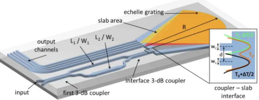
The proposed temperature-insensitive (athermal) echelle grating filter is schematically shown in Fig. 1. The temperature synchronized Mach-Zehnder interferometer (MZI) placed at the entrance to the slab area is made of two 3-dB directional couplers (marked as first and interface couplers in the figure) and two unbalanced branches with lengths L1and L2and widths w1and
w2, respectively. Different waveguide widths allow varying the effective thermo-optic coefficients
of the two waveguide branches, thus precisely controlling the dependence of the MZI behaviour on temperature [13, 15]. As depicted in Fig. 1,the coupled waveguides of the interface 3-dB coupler form the input to the echelle filter and, driven by the temperature-dependent phase delays in the MZI, generate a field distribution at the interface that shifts with temperature. The shift of field peak position is designed to match the thermal dispersion of the echelle grating over a selected temperature range ∆T and thus ensures that the field reflected by the grating at a given wavelength is imaged on the same output waveguide for all temperatures. To achieve a temperature-independent behavior for all the wavelength channels of the echelle filter, the MZI is designed to have a large FSR, minimizing the roll-off of its transfer function over the full
Fig. 1. Schematic of the SOI athermal echelle grating with a temperature-synchronized Mach-Zehnder input for temperature-insensitive operation. The inset shows the designed changes of the optical field with temperature at the entrance of the slab area.
operational bandwidth and hence ensuring that the field generated at the entrance of the slab area is the same for all the channels.
As a proof-of-concept, we consider a standard SOI technology with a 220-nm silicon core thickness and silicon dioxide upper and lower claddings. The echelle grating is designed to have four channels with 800 GHz spacing centered around λ0= 1550 nm and 1-dB bandwidth
of about 140 GHz. The grating is in a Rowland circle configuration with a radius of 250 µm, a diffraction order of 20, and a mounting angle of 45 degree. The choice of a small Rowland circle radius helps reducing the impact of the silicon thickness inhomogeneity as pointed out in [3, 6]. As will be discussed in later sections, small dimensions are also advantageous for the compensation of the thermo-optic effects. The angular dimension of the grating is 15 degree in order to capture the entire field of the T-synced input. The reflectance of the grating facets is assumed to be 100% in the simulations. High reflectance can be achieved in practice exploiting Bragg reflectors [6]. At the Rowland circle waveguides have a width of 2 µm and are then tapered to 500 nm to ensure single-mode propagation. With the employed 220-nm silicon core with oxide cladding, the temperature-induced angular shift of the echelle grating is 0.0076 deg/K (see Eq. (1)). The corresponding spacial shift is approximately 950 nm over a 20 K temperature range.
Key considerations for the design of the complete device are athermal operating temperature range, overall device size, excess loss and tolerance to fabrication uncertainties. The design of the Mach-Zehnder interferometer is presented in Sec. 2.1 while Sec. 2.2 discusses in detail the design of the coupler at the interface with the slab area. The electromagnetic simulations presented in the next sections for the Mach-Zehnder were obtained with a commercial finite difference mode solver and a 3D mode expansion propagation solver [20]. The design and simulation of the echelle grating were performed with a dedicated 2D semi-vectorial in-house tool based on the Huygens-Kirchhoff diffraction theory and the effective index approximation. The software can handle input fields of arbitrary and strongly dispersive shapes as could be possibly generated by some T-synced input configurations.
2.1. Design of the Mach-Zehnder interferometer
During the design of the MZI, we considered for the first 3-dB coupler a width of 500 nm for both waveguides and a gap of 300 nm, obtaining a 3-dB length Lf = 46 µm. Interconnecting
waveguide sections were assumed to have the same length in the two MZI branches and a width of 500 nm, thus not contributing to the overall transfer function. The design was performed by defining for each branch a section of length L1and L2and width w1and w2, respectively, to
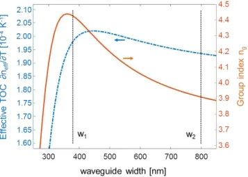
Fig. 2. Effective thermo-optic coefficient (TOC) and group index for the fundamental TE-like mode of an SOI waveguide as function of the waveguide width. The dashed lines mark the chosen widths w1= 380 nm and w2= 800 nm.
cross condition (or vice-versa) within the given temperature variation ∆T to match the echelle focal spot shift with temperature.
Assuming a linear frequency dispersion around the central wavelength λ0, the FSR of the
Mach-Zehnder (in wavelength) is defined as
F S R = λ
2 0
L1ng,1(λ0, T0) − L2ng,2(λ0, T0)
(2) where λ0and T0are the central wavelength and temperature of the considered ranges, Liis the
length of the waveguide (i=1,2), and ng,i(λ0, T0) is the group index of the i-th waveguide at λ0
and T0. The FSR can hence be easily maximized imposing that
L1ng,1(λ0, T0) = L2ng,2(λ0, T0). (3)
In order to match the temperature dispersion of the echelle grating, the phase difference between the modes propagating in the two branches of the MZI must change between -π/2 and π/2 when the temperature varies from T0-∆T/2 to T0+∆T/2. Assuming a linear dependence of the phase
effective index on temperature, this condition is equivalent to L1∂neff,1(λ0, T ) ∂T T0 ∆T − L2 ∂neff,2(λ0, T ) ∂T T0 ∆T = λ0 2 (4)
with neff,i(λ0, T ) the temperature-dependent phase effective index of the i-th waveguide at central
wavelength λ0. Although the same behaviour could be obtained varying the phase difference
between π/2 and 3π/2, this would cause the field at the output of the MZI to be anti-symmetric, with detrimental effects for both the propagation in the slab area and the overlap with the output waveguide. This condition is avoided in the design and the analysis of fabrication uncertainty discussed in Sec. 3 ensures it is not reached with linewidth uniformity guaranteed by standard fabrication technologies.
Equations (3) and (4) allow to calculate the lengths L1and L2for any chosen combination
of w1and w2in order to simultaneously maximize the FSR and match the shift of the grating
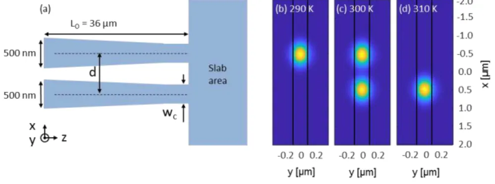
Fig. 3. (a) Schematic of the interface 3-dB coupler. (b-d) Field profile |Ex|2for λ = 1550
nm at the entrance to the echelle slab area for temperature of 290 K, 300 K and 310 K, respectively.
TE-like mode of an SOI waveguide was simulated as function of waveguide width, temperature and wavelength. To model silicon properties, we considered at λ = 1550 nm and T = 300 K a refractive index of 3.479, a thermo-optic coefficient of 1.87×10⁻⁴K−1and a spectral dispersion of -0.083 µm−1.The same parameters for silica were chosen as 1.444, 0.85×10⁻⁵K−1and -0.012 µm−1, respectively [21] . From these simulations, the dependence of the group index ngand
the (effective) thermo-optic coefficient ∂neff/∂T on waveguide width were calculated. Figure 2
shows the obtained results for λ0= 1550 nm and T0= 300 K.
There are several considerations for choosing w1and w2. An MZI with w1< 350 nm and w2>
500 nm (or vice-versa) maximizes the difference between the two thermo-optic coefficients and the two group indices, which together contributes in defining the required lengths of the branches through Eqs. (3) and (4). Consequently this would reduce L1and L2and the overall device size.
On the other hand, this choice would make the device very sensitive to fabrication uncertainties because of the steep dependence of both ngand ∂neff/∂T on waveguide width for w < 350 nm. In
the proposed design we hence chose w1= 380 nm and w2= 800 as a viable compromise between
robustness and device compactness (dashed lines in Fig. 2). In this case ∂neff,1/∂T = 1.981×10⁻⁴
K−1, ∂neff,2/∂T = 1.936×10⁻⁴K−1, ng,1= 4.426, and ng,2= 3.909 for T0= 300 K and λ0= 1550
nm. For an athermal operating temperature range ∆T = 20 K, the corresponding lengths of the two branches obtained with Eqs. (3) and (4) are L1= 1707 µm and L2= 1933 µm. The choice of
the temperature range is discussed in Sec. 2.2. 2.2. Design of the coupler-slab interface
The design of the 3-dB directional coupler at the interface with the echelle slab area is particularly important for minimizing the excess loss generated by replacing a simple input waveguide with the proposed T-synced input. It should be noted that the modal mismatch between the coupler and the slab area also generates back-reflections that might be critical for certain applications and should hence be minimized. A schematic of the directional coupler and interface section is shown in Fig. 3(a). Here the design parameters are the waveguide distance d and the waveguide width wc. The goal is to match the focal point shift with temperature in the echelle for as large a
temperature range as possible, while maximizing the modal overlap between the field generated by the T-synced input (and imaged by the grating to the echelle outputs) and the fundamental mode of the 2-µm-wide output waveguides.
To this purpose, the distance d must be equal to the shift produced by the echelle slab over the selected temperature range ∆T. A small value of d is desirable to both improve the overlap with the output mode and reduce the length of the 3-dB interface coupler. Since the echelle
angular shift with temperature is determined by the thermo-optic properties of the slab waveguide according to Eq. (1), a small d can be achieved by reducing the Rowland radius. On the other hand, considerations for example on channel cross-talk, grating truncation loss and fabrication issues limit the minimum radius usable. As a balanced choice, we selected a Rowland radius R = 250 µm that for a temperature range ∆T = 20 K centered at 300 K is expected to generate a focal point shift of 950 nm, which is hence chosen as value for d.
Overlap losses and back-reflections depend on wcin two opposite ways. Narrow waveguides
are required to expand the field profile in the horizontal direction and improve the in-plane overlap with the fundamental mode of the echelle output. On the other hand, narrow waveguides delocalize the field also in the vertical direction, decreasing the out-of-plane overlap and increasing the back-reflections. For our design, wc= 255 nm represents a good compromise, giving an
overlap loss with the fundamental mode of a 2-µm waveguide at T0= 300 K of about 0.7 dB and
back-reflections smaller than -14 dB. The increase of the overlap losses at T = 290 K and T = 300 is smaller than 0.4 dB. Two 35-µm-long linearly tapered sections were used to adiabatically adjust the width from the initial 500 nm to wc= 255 nm with negligible losses. A total coupler
length LO= 36 µm (including tapers) ensures a 3-dB operation at λ0= 1550 nm and T0= 300 K.
As an example, Figs. 3(b)-3(d) shows the simulated field profile |Ex|2generated at the entrance
to the slab area by the interface coupler at temperature 290 K, 300 K and 310 K, respectively. For these simulations, we assumed the fundamental quasi-TE modes being excited at the beginning of the two 500 nm wide waveguides with the same power and a phase difference of -π/2 rad, 0 rad and π/2 rad respectively, as generated by the Mach-Zehnder designed in section 2.1 for the three considered temperatures. As expected, the center of the spot shifts about 950 nm with a temperature variation of 20 K. The field shape also changes with temperature, causing a slight variation of the shape of the echelle pass-bands as described in the next section.
3. Athermal echelle simulations and performance
For the evaluation of the entire device we considered the parameters optimized in the previous sections: ∆T = 20 K centered at T0= 300 K; central wavelength λ0= 1550 nm; for the first 3-dB
coupler, Lf = 46 µm, waveguide width 500 nm and gap 300 nm; for the MZI branches w1= 380
nm, w2 = 800 nm, L1 = 1707 µm, and L2= 1933 µm; for the interface 3-dB coupler d = 950
nm, wc= 255 nm and length LO= 36 µm; a waveguide width of 2 µm for the echelle output
waveguides. The simulation of the entire T-synced input was performed exploiting a transfer matrix approach, describing its transmission as a function of wavelength and temperature as [17]
M(λ, T ) = e−jϕso 0 0 e−jϕoa · C · e−jβ1L1 0 0 e−jβ2L2 C−1· e−jβsfLf 0 0 e−jβafLf · C · 1 0 (5)
where βs/af are the propagation constants of the symmetric and anti-symmetric modes of the first coupler (length Lf) while β1and β2are the propagation constants of the two branches of the
Mach-Zehnder (lengths L1and L2). The phase delay of the symmetric and anti-symmetric modes
of the interface coupler are defined as ϕo s/a=
∫LO
0 β
o
s/a(s) ds, where LOis the length of the output
coupler and βo
s/athe propagation constants of the two modes. The integral is required because
βo
s/achange along the coupler due to the tapered sections. Propagation losses are omitted. The
matrix C is defined as C = 1 1 1 −1 (6) and is needed to convert transfer matrices defined on the fundamental modes of isolated waveguides to matrices defined on the symmetric and anti-symmetric modes of the couplers. All
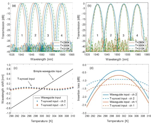
Fig. 4. Simulations of the transfer functions of the four echelle filter channels with (a) a conventional 2-µm waveguide input and (b) ) using the proposed temperature-synchronized input. The numerals denote the channel number. (c) Channel wavelength shift as a function of temperature in the case of waveguide input (black solid line - the same for all the channels) and T-synced input (red diamonds and blue crosses for channels 1 and 2, respectively). (d) Insertion loss for channels 1 and 2 calculated at the channel central wavelength at 300 K.
the propagation constants β in Eq. (5) were simulated as function of wavelength and temperature as described in Sec. 2. It is worth noting that in this way the simulations take into account the dependence of the transfer function with wavelength and temperature not only for the two MZI branches but also for the two 3-dB couplers, providing an accurate result for the entire input circuit. Matrix M was used to compute the field profile at the entrance to the slab area, and the transfer function of the echelle filter was then computed with our in-house tool using these fields as input.
The simulation results are presented in Fig. 4. As a reference, Fig. 4(a) shows the transmission spectra obtained with a conventional simple 2-µm-wide input waveguide for the four channels of the echelle grating at 290 K, 300 K and 310 K, respectively. At 300 K, the four channels are located at λ1= 1540.56 nm, λ2= 1546.92 nm, λ3= 1553.33 nm, and λ4= 1559.80 nm. Channel
3-dB bandwidth is about 250 GHz. The minimum insertion loss is 0.4 dB, the power roll-off is about 0.3 dB and channel cross-talk is smaller than -35 dB. By using the proposed T-synced input, the spectral shift is significantly reduced, as shown in Fig. 4(b). This design modification introduces a slight dependence of the pass-band on temperature due to the variation of the corresponding field distribution generated at the entrance to the slab area (see Figs. 3(b)-3(d)). Channel cross-talk slightly increases only at the edges of the design temperature range.
Figure 4(c) shows the shift of the central wavelength of the channels. For the conventional waveguide input, a linear shift with temperature of approximately 1.6 nm over the 20-K temperature
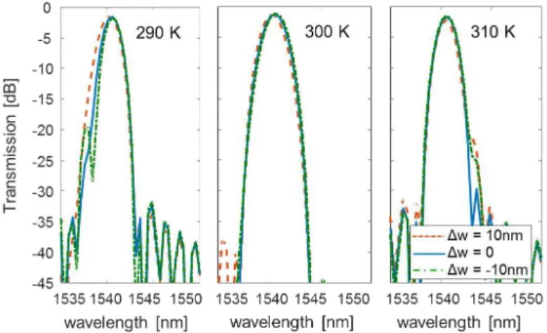
Fig. 5. Worst-case fabrication tolerance analysis: pass-band of outer channel 1 (λ1= 1540.56
nm) at 290 K, 300 K, and 310 K, respectively, with a waveguide width deviation of ±10 nm in the T-synced input.
range (or 80 pm/K, see the black solid line) is observed. For the T-synced input case, red diamonds and blue crosses report the residual wavelength shift for channels 1 and 2. Channels 3 and 4 have similar properties and are omitted here for clarity. As can be seen, there is a residual zero-mean fluctuation of the channel spectral position with temperature. This is due to the fact that the "center-of-gravity" of the field distribution generated by the MZI depends on temperature through a squared sine function. The maximum of the average residual fluctuation is about ±45 pm at 295 K and 305 K.
Lastly, Fig. 4(d) reports the insertion loss for channels 1 and 2 at their central wavelengths λ1
= 1540.56 nm and λ2= 1546.92 nm, respectively, for both the waveguide and T-synced input
cases. Results are similar for channels 3 and 4. With a conventional waveguide input, central channels (2 and 3) have an insertion loss of about 0.4 dB at 300 K that quickly increases to more than 2 dB with temperature variations of ±10 K due to the shift of the pass-band. The use of the T-synced input increases the insertion loss at 300 K for these channels to about 0.9 dB due to the additional overlap losses with the fundamental mode of the 2-µm output waveguide. On the other hand, this insertion loss has a much smaller dependence on temperature and reaches only 1.3 dB at 290 K and 310 K. In this case the additional losses mainly come from a slight residual wavelength dependence of the Mach-Zehnder transfer function and hence of the field generated at the entrance of the slab area. For both types of input designs, the outer channels (1 and 4) have behavior similar to the central channels but with an additional loss of about 0.3 dB due to the power roll-off of the echelle grating.
The careful selection of the waveguide width for the two Mach-Zehnder branches presented in Sec. 2.1 and the balanced design of the interferometer provide a good robustness of the proposed device to fabrication errors. In order to test this sensitivity we repeated the simulations assuming a variation ∆w = ± 10 nm of the waveguide width in the MZI, including both 3-dB couplers and the two branches. This range of dimensional changes well represents the expected linewidth uniformity with 193 nm deep-UV lithography [22]. The dimensions of the echelle grating are kept unchanged as variations on this scale on the grating facet positions do not significantly change the filter performance, causing at most a slight increase of the channel cross-talk. Figure 5 reports the simulation results along with the ideal response (∆w = 0, same data shown in Fig. 4(b)) for channel 1 at 290 K, 300 K, and 310 K, respectively. Since the entire MZI design is performed at the central wavelength 1550 nm, the outer channels 1 and 4 are expected to suffer
more spectral distortion compared to the central channels 2 and 3. As can be seen, the device exhibits a good tolerance to fabrication uncertainties. The effect of the waveguide width variation on the pass-band shape and central wavelength are negligible at the center of the considered temperature range (300 K). At the edges (290 K and 310 K) the compensation of the thermal shift of the transfer function is still effective, preserving the functionality of the device, with some minor effects on the shape of the pass-band. Similar results were obtained for channel 4 while channel 2 and 3 showed an expected higher tolerance to waveguide width deviations, with negligible effects also at 290 K and 310 K. The same device tolerance is predicted also considering waveguide width deviations between the two branches that are uncorrelated but within the same range.
4. Conclusions
We have proposed a design for an athermal echelle grating filter operating in TE polarization that relies exclusively on standard silicon-on-insulator photonics fabrication processes without using any additional material with negative thermo-optic coefficient. The device exploits a Mach-Zehnder interferometer with a very large free spectral range as a temperature-synchronized input of the echelle grating to match the shift of the grating focal point with temperature. In this way, a large reduction of the sensitivity of the overall transfer function with temperature has been achieved, with a residual zero-mean fluctuation of about ±45 pm over a temperature range of 20 K compared to a 1.6-nm shift obtained with a simple waveguide input. The use of the Mach-Zehnder at the input slightly increased the device insertion loss by about 0.5 dB. The device functionality has been numerically demonstrated taking into account also a waveguide width fabrication uncertainty of ±10 nm. The covered temperature range could be increased by further minimizing the radius of the echelle grating and by exploiting different types of interface couplers (e.g. multi-mode interference couplers).
References
1. X. Guan, X. Wang, and L. H. Frandsen, “Optical temperature sensor with enhanced sensitivity by employing hybrid waveguides in a silicon mach-zehnder interferometer,” Opt. Express 24, 16349–16356 (2016).
2. D. Melati, A. Waqas, A. Alippi, and A. Melloni, “Wavelength and composition dependence of the thermo-optic coefficient for ingaasp-based integrated waveguides,” J. Appl. Phys. 120, 213102 (2016).
3. K. Okamoto, “Progress and technical challenge for planar waveguide devices: silica and silicon waveguides,” Laser & Photonics Rev. 6, 14–23 (2011).
4. C. R. Doerr and K. Okamoto, “Advances in silica planar lightwave circuits,” J. Light. Technol. 24, 4763–4789 (2006). 5. S. Janz, A. Balakrishnan, S. Charbonneau, P. Cheben, M. Cloutier, A. Delage, K. Dossou, L. Erickson, M. Gao, P. A. Krug, B. Lamontagne, M. Packirisamy, M. Pearson, and D. X. Xu, “Planar waveguide echelle gratings in silica-on-silicon,” IEEE Photonics Technol. Lett. 16, 503–505 (2004).
6. S. Pathak, P. Dumon, D. V. Thourhout, and W. Bogaerts, “Comparison of awgs and echelle gratings for wavelength division multiplexing on silicon-on-insulator,” IEEE Photonics J. 6, 1–9 (2014).
7. S. Kamei, T. Kitoh, M. Itoh, T. Shibata, and M. Kohtoku, “50-ghz-spacing athermal mach-zehnder interferometer-synchronized arrayed-waveguide grating with improved temperature insensitivity,” IEEE Photonics Technol. Lett. 21, 1205–1207 (2009).
8. S. Namnabat, K.-J. Kim, A. Jones, R. Himmelhuber, C. T. DeRose, D. C. Trotter, A. L. Starbuck, A. Pomerene, A. L. Lentine, and R. A. Norwood, “Athermal silicon optical add-drop multiplexers based on thermo-optic coefficient tuning of sol-gel material,” Opt. Express 25, 21471–21482 (2017).
9. S. Grillanda, V. Raghunathan, V. Singh, F. Morichetti, J. Michel, L. Kimerling, A. Melloni, and A. Agarwal, “Post-fabrication trimming of athermal silicon waveguides,” Opt. Lett. 38, 5450–5453 (2013).
10. J. H. Schmid, M. Ibrahim, P. Cheben, J. Lapointe, S. Janz, P. J. Bock, A. Densmore, B. Lamontagne, R. Ma, W. N. Ye, and D.-X. Xu, “Temperature-independent silicon subwavelength grating waveguides,” Opt. Lett. 36, 2110–2112 (2011).
11. S. S. Djordjevic, K. Shang, B. Guan, S. T. S. Cheung, L. Liao, J. Basak, H.-F. Liu, and S. J. B. Yoo, “Cmos-compatible, athermal silicon ring modulators clad with titanium dioxide,” Opt. Express 21, 13958–13968 (2013).
12. J.-J. He and E. S. Koteles, “Athermal waveguide grating based device having a temperature compensator in the slab waveguide region,” (2001). US Patent 6,169,838.
13. M. Uenuma and T. Motooka, “Temperature-independent silicon waveguide optical filter,” Opt. Lett. 34, 599–601 (2009).
14. B. Guha, K. Preston, and M. Lipson, “Athermal silicon microring electro-optic modulator,” Opt. Lett. 37, 2253–2255 (2012).
15. K. Hassan, C. Sciancalepore, J. Harduin, T. Ferrotti, S. Menezo, and B. B. Bakir, “Toward athermal silicon-on-insulator (de)multiplexers in the o-band,” Opt. Lett. 40, 2641–2644 (2015).
16. C. R. Doerr, L. W. Stulz, R. Pafchek, and S. Shunk, “Compact and low-loss manner of waveguide grating router passband flattening and demonstration in a 64-channel blocker/multiplexer,” IEEE Photonics Technol. Lett. 14, 56–58 (2002).
17. C. R. Doerr, L. W. Stulz, and R. Pafchek, “Compact and low-loss integrated box-like passband multiplexer,” IEEE Photonics Technol. Lett. 15, 918–920 (2003).
18. S. Kamei, T. Shibata, and Y. Inoue, “Compensation for second-order temperature dependence in athermal arrayed-waveguide grating realizing wide temperature range operation,” IEEE Photonics Technol. Lett. 21, 1695–1697 (2009).
19. P. Cheben, A. Delage, S. Janz, and D.-X. Xu, “Echelle and arrayed waveguide gratings for wdm and spectral analysis,” in Advances in information optics and photonics, (2008), chap. 29, pp. 599–632.
20. Lumerical Inc. http://www.lumerical.com/.
21. D. B. Leviton and B. J. Frey, “Temperature-dependent absolute refractive index measurements of synthetic fused silica,” Proc. SPIE 6273, 6273–6284 (2006).
22. D. X. Xu, J. H. Schmid, G. T. Reed, G. Z. Mashanovich, D. J. Thomson, M. Nedeljkovic, X. Chen, D. V. Thourhout, S. Keyvaninia, and S. K. Selvaraja, “Silicon photonic integration platform - have we found the sweet spot?” IEEE J. Sel. Top. Quantum Electron. 20, 189–205 (2014).