HAL Id: hal-00459474
https://hal.archives-ouvertes.fr/hal-00459474
Submitted on 24 Feb 2010
HAL is a multi-disciplinary open access
archive for the deposit and dissemination of
sci-entific research documents, whether they are
pub-lished or not. The documents may come from
teaching and research institutions in France or
abroad, or from public or private research centers.
L’archive ouverte pluridisciplinaire HAL, est
destinée au dépôt et à la diffusion de documents
scientifiques de niveau recherche, publiés ou non,
émanant des établissements d’enseignement et de
recherche français ou étrangers, des laboratoires
publics ou privés.
Vapor-liquid-solid mechanisms: Challenges for nanosized
quantum cluster/dot/wire materials
Pierre Cheyssac, M. Sacilotti, G. Patriarche
To cite this version:
Pierre Cheyssac, M. Sacilotti, G. Patriarche. Vapor-liquid-solid mechanisms: Challenges for nanosized
quantum cluster/dot/wire materials. Journal of Applied Physics, American Institute of Physics, 2006,
100 (044315), pp.044315-1. �10.1063/1.2236163�. �hal-00459474�
Vapor-liquid-solid mechanisms: Challenges for nanosized quantum
cluster/dot/wire materials
P. Cheyssaca兲
Laboratoire de Physique de la Matière Condensée, UMR6622-CNRS 6622, Université de Nice-Sophia Antipolis, Parc Valrose, F-06108 Nice Cedex 2, France
M. Sacilotti
Groupe Couches Minces et Nanostructures, UFR Sciences et Techniques FR 2604, Université de Bourgogne, 9 Avenue A. Savary, BP 47870, 21078 Dijon Cedex, France
G. Patriarche
Laboratoire de Photonique et de Nanostructures, UPR20-CNRS, Route de Nozay, 91460 Marcoussis, France
共Received 15 June 2005; accepted 30 June 2006; published online 25 August 2006兲
The growth mechanism model of a nanoscaled material is a critical step that has to be refined for a better understanding of a nanostructure’s dot/wire fabrication. To do so, the growth mechanism will be discussed in this paper and the influence of the size of the metallic nanocluster starting point, referred to later as “size effect,” will be studied. Among many of the so-called size effects, a tremendous decrease of the melting point of the metallic nanocluster changes the physical properties as well as the physical/mechanical interactions inside the growing structure composed of a metallic dot on top of a column. The thermodynamic size effect is related to the bending or curvature of chains of atoms, giving rise to the weakening of bonds between them; this size or curvature effect is described and approached to crystal nanodot/wire growth. We will describe this effect as that of
a “cooking machine” when the number of atoms decreases from⬃1023at./ cm3for a bulk material
to a few tens of them in a 1 – 2 nm diameter sphere. The decrease of the number of atoms in a metallic cluster from such an enormous quantity is accompanied by a lowering of the melting temperature that extends from 200 up to 1000 K, depending on the metallic material and its size under study. In this respect, the vapor-liquid-solid共VLS兲 model, which is the most utilized growth mechanism for quantum nanowires and nanodots, is critically exposed to size or curvature effects 共CEs兲. More precisely, interactions in the vicinity of the growth regions should be reexamined. Some results illustrating the growth of micrometer-/nanometer-sized materials are presented in order to corroborate the CE/VLS models utilized by many research groups in today’s nanosciences world. Examples of metallic clusters and semiconducting wires will be presented. The results and comments presented in this paper can be seen as a challenge to be overcome. From them, we expect that in a near future an improved model can be exposed to the scientific community.
I. INTRODUCTION
Nanosized materials, of great interest for the future and more efficient everyday devices and machines, experience mechanical, electrical, and optical properties modified by quantum confinement. Their development requires an im-provement of our knowledge on both growth techniques and growth mechanisms that take place when building nanosized dots and wire/tube shaped three-dimensional structures, re-ferred hereafter as 3D-Ss, although it is more appropriate for balloons than for wires and quantum dots since they are
closer to one-dimensional structures 共1D-Ss兲 than wires.
Among nanocolumn structures, one finds empty tubes such
as carbon nanotubes and wires or rods.1,2 Many research
groups utilize as catalysts metallic nanosized cluster
materi-als共diameter d from 1 to 50 nm兲 as the “cooking machine”
for building the whole structure of three-dimensional 共3D兲
edifices, composed of a column topped by a nanosized
clus-ter maclus-terial.2–6 Others groups mention noncatalytic 3D-S
growth.7,8 “Self-catalysts” have been also reported to grow 3D-S by using organometallic compounds that interact with many kinds of metallic, semiconductor, and insulating materials.9–11One clearly sees that 3D shaped structures will be different according to the method of their fabrication, and that different applications can result from such diversities of structures.
Wire shaped materials have been realized since 1964, after Wagner and Ellis’s work on the growth of
micrometer-sized semiconductor materials.12 In their growth model,
“food nutrients” are chemical elements that will be incorpo-rated in the 3D-S through a catalysis effect due to the action of a “cooking agent,” a gold metallic cluster. In other words, a micrometer-sized metal cluster acts as a catalyst, trans-forms food nutrients, and builds the 3D-S. The concept
be-hind this model was a vapor-liquid-solid 共VLS兲 mechanism
in which the growth of 3D-S takes place by volume diffusion
of transformed nutrients through the metallic catalyst cluster that builds the whole structure. In 1975, Givargizov’s work proposed that the VLS model consisted of four steps, the more important being that which controls the metal cluster/ column growths at their interface.13In this model, the growth
environment can be physical vapor deposition 共PVD兲 or
chemical vapor deposition 共CVD兲.12,13 More recently a
chemistry research group, led by Buhro and co-workers, has shown that the VLS growth mechanism could be adapted to 3D-S growth in solution ambient and proposed the
solution-liquid-solid 共SLS兲 mechanism.14–16 In some of their work,
Trentter et al. used nanosized decomposed metal-organic molecules for growing semiconductor materials at tempera-tures of 200– 400 K below the current PVD or CVD process temperature.14
In the race for more efficient building processes and the need for nanosized structures, the micrometallic cluster has
reached the nanometer range.4,6,8,12,14 The physical and
chemical properties of the cooking agent, the metallic clus-ter, are more or less modified by this reduction in size but many of the nanosized structure makers do not take such effects into account. Among these size effects, one finds cata-lytic properties whose efficiency may change with crystallo-graphic faces of the metallic cluster, movement of its crys-tallographic planes and surface atoms, and the decrease of its melting temperature Tm with size.17 Catalysis and diffusion
are still parts of the previous growth models; their improve-ment and a better understanding of the existing experiimprove-mental results should result if one takes such size effects into ac-count. Wagner and Ellis12and Givargizov,13as well as more modern descriptions of growth methods such as
metal-organic CVD 共MOCVD兲,8chemical beam epitaxy共CBE兲,5,6
laser catalytic growth共LCG兲 mechanism,4and SLS,14–16 as-sume that the metallic cluster/column interface is flat; how-ever, size effects or the physical state of the cluster itself 共solid or liquid兲 may affect its curvature. The decrease of the melting temperature Tmwith the size of the metallic cluster
has been studied by Buffat’s work that applied the
Gibbs-Thomson equation to relate Tmto the diameter of small and
spherical metallic particles.17Kofman and co-workers
dem-onstrated that not only the diameter of the dot but also its shape, described by curvatures, modifies Tm.18,19Then, the
physical state and shape of the metallic cluster depend on its size. Such effects seem forgotten or not taken into account by many nanosized crystal growers.
The aim of this paper is to discuss the influence of me-tallic cluster size, shape, and state on the growth of 3D-S, related to some of our grown structures. Size effects involved in this paper are physical parameters such as Tm,
crystallo-graphic structure of the metallic cluster, mobility of its sur-face atoms, flatness of the cluster/column intersur-face, diffusion
of atoms 共metallic cluster or column nutrients兲, and vapor
pressure, due to the curvature of the metallic cluster surface. This paper will take into account most of the debated refer-enced works presented above; it will present the influence of size/shape effects upon the VLS mechanism and will propose some paths for research in the field of quantum dot and wire semiconductor materials to overcome the presently debated results. The flat cluster/column interface model by Wagner
and Ellis and followed by most of cluster/column or tube growers is presently questioned.4–8,12–16 Inside the commu-nity debating the VLS/SLS models, recent results by Sam-uelson and co-workers led to the questioning of the diffusion through the metallic cluster and proposal of a more
conve-nient surface reaction limited growth model.20,21 Melting
temperature modified by the cluster size and shape, but not taken into account by most of modern wire growers, should
also be taken into account.22,23 Throughout this paper and
references therein the word column will refer to wire, rod, or tube and cluster to metallic aggregates used as the cooking system helping to build the 3D-S. This 3D-S will refer to a column and a metallic cluster on top of it.
This paper is organized as follows:共a兲 Some aspects of
the VLS mechanism model and its drawbacks will be
pre-sented. 共b兲 Shape/size effects will be exposed, and results
about many metals catalysts presented.共c兲 Suggestions for a more convenient dot/rod interface model will be given, sup-ported by some recent results about catalyst/noncatalyst 3D-S growth.
II. THE MODEL OF THE VLS„SLS, VSS, ETC.… MECHANISM
Demonstrated by Wagner and Ellis’s work and followed by many other 3D-S growers such as Givargizov, Lieber, Samuelson, and Buhro, the Vapor-liquid-solid mechanism is briefly described below.2–16Although this paper focuses on
VLS and vapor-solid-solid 共VSS兲 mechanisms, it is
worth-while to mention that there exist other possibilities. Carbon tubes have been grown without metallic cluster but with
fer-rocene as catalyst.24 Oxide assisted growth has also been
performed.25,26
For the first step of the VLS mechanism, a metallic layer or cluster is deposited at the surface of a flat substrate; with or without annealing, metallic aggregates or clusters form on this surface. Then, in this model, the flat interface that may exist between the cluster and the growing column comes from the existing one at the beginning of the process. In the second step, the surface is fed with nutrients in a PVD or CVD, assisted or not, environment. In liquid solutions, me-tallic particles can be added to the solution or created in situ by chemical reactions.14–16According to this model, the nu-trients cross the dot’s metallic structure by diffusion and build an empty or filled column that is considered nowadays as a wire, nanowire, nanorod, or nanotube. The interface
be-tween the metallic cluster 共d⬃10–50 nm兲 and the column
共dc⬃10–50 nm兲 has always been considered as flat,2–6,12–16
the main reason for this being that 3D-S results from an almost perfectly flat heteroepitaxy,20,21 as shown by
high-resolution transmission electron microscopy 共HRTEM兲
pic-tures obtained after the 3D-S growth. In this respect, it would be very interesting to monitor the curvature of the interface during the growth process.
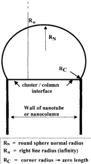
Figure 1 summarizes the existing VLS growth model, as
depicted above. Figure 2 shows a truncated sphere共metallic
cluster兲 on top of a column, separated by a flat interface. Three radii of curvature can be considered: RN, the radius of
curvature of a flat interface between the cluster and the
grow-ing column 关both are not supposed to be questioned since
they represent, respectively, the sphere共a few tens of nanom-eters兲 and the radii of curvature of the cluster column as-sumed as a flat interface兴; and Rc, the radius of the contact
line or corner zone between the truncated metallic sphere and the flat interface. We leave apart the radius of the column that supports the interface.
Within the VLS model, the problem starts when consid-ering Rc: if it approaches zero or the interatomic distance,
thermodynamic size or curvature effects should strongly ap-ply. In the metallic truncated sphere, regions described
es-sentially by Rc present a melting temperature much lower
than in the rest of the sphere.18,19Let us take the example of
a gold cluster whose bulk melting point is TB⬃1336 K;
Tm共Rc⬃1.5 nm兲⬃765 K and Tm reaches room temperature
for Rc⬃0.8 nm. Around RN⬃2.5 nm, Tmchanges very
rap-idly. When RN goes from 10 to 2.5 and 1.65 nm, Tm共RN
⬃10 nm兲=1261 K, Tm共RN⬃2.5 nm兲=1080 K, and Tm共RN
⬃1.65 nm兲=934 K. One can evaluate the amplitude of these changes with RNthrough the relative variation of the melting
temperature ⌬Tm/ TB=共TB− Tm兲/TB which takes the
follow-ing values: 5.55⫻10−2, 19.1⫻10−2, and 30.09⫻10−2,
respectively.17
If the VLS model is to remain with a cluster/column flat interface and a corner shaped gold cluster, its current state, then the corner contact line should be melted even at room temperature when Rc⬍1.65 nm.17In this case, wetting
con-ditions of the liquid part of the cluster onto the interface give rise to a contact angle that will determine the external shape of the gold cluster. This model should also present a local zone hotter than the others: the “cooking zone” is appropri-ated for building a columnar structure or a meniscus seeming like the one seen for bulk crystal growth from its liquid
phase.27 Under these conditions, we enumerate below some
points of the VLS model mechanism that may be criticized. • The corner zone which is the external contact line that limits the flat interface between the truncated cluster and the column experiences a local decrease of the melting temperature of the supported metallic cluster due to curvature effects.
• A flat interface between the metallic cluster and the
growing column is assumed once the growth process is running. Arguments are given below for other possi-bilities.
• Also, no physical reason justifies the existence of such flat interface between the metallic cluster and the mono- or multiwalled empty carbon column.
• More recently, Samuelson and co-workers have
claimed a surface reaction mechanism instead of a vol-ume diffusion limited reaction through the metallic cluster.21,28
The first criticism has been examined above. Concerning the second one, in fact, physical requirements can be brought into play to clarify the assumption of a strictly flat cluster-column interface. When two different materials, substrate and deposited cluster, are in contact, their common interface is an interaction zone, and each material exerts forces on the other one. These forces are interfacial tensions and determine the possibility of wetting of one material onto the other as well as the external shape of the contactless zones共Fig. 2兲. Wetting exists for solids as well as for liquids. If the sub-strate, i.e., in our case the column, is not rigid enough be-cause of its thickness or its mechanical properties, its inter-face in contact with another material will be bent by the interfacial tensions exerted by this material. Then R⬀can no longer be considered as infinite.29–31 Also, the equilibrium between the various interfacial tensions governs the contact angle or wetting angle between the cluster and the column and also its external shape.32 This concept of wetting angle remains valid even for small sizes as considered here.33
The description of the cluster-column interface should then be improved in the following way: for most metallic
cluster and growing column materials utilized, R⬀ 共Fig. 2兲
becomes finite and a characteristic contact angle is present FIG. 1. A schematic representation model of the VLS mechanism: PVD or
CVD growth of a nanotube/nanocolumn, starting from a metallic cluster and ending by a wire capped by a metallic cluster.
FIG. 2. The VLS mechanism; geometry of the existing metallic cluster/ column flat interface associated with the radii of curvature.
between the metallic cluster 共or crystal兲 and the column. Moreover, the previous external contact line should not re-main as a circle on a flat interface with Rc⬃0 but becomes a
transition zone associated with Rclarger than the interatomic
distance of the cluster atoms.
During the very beginning of growth, if the substrate is flat, the cluster already on the substrate shares a flat interface with it before the column growth starts. Unless both cluster and column realize a perfect epitaxial contact at their inter-face, stresses are present due to interfacial energies and tend to bend this interface during the growth process. As a con-sequence, other phenomena should be invoked if one wants to keep a flat cluster-column interface during the growth pro-cedure.
This debate can help in building a VLS growth mecha-nism physically current and acceptable. It will be developed below.
III. SOME 3D STRUCTURES GROWN BY MOCVD WITH ORGANOMETALLIC MOLECULES ONLY
MOCVD has been used since 1967 and crystal growers have since then discussed for many years metallic droplets that occur during high ratio growth conditions of III/V
compounds.34,35 The same effect holds for the molecular
beam epitaxy 共MBE兲 and other related techniques.36
Recently, 3D-Ss presenting top to bottom interfaces with other shapes have been grown by simply using the interac-tion of organometallic precursor molecules with substrates. These results are presented below, accompanied by informa-tion about size and curvature effects for the most commonly used metallic clusters.
Sacilotti et al. have shown that, if group V hydrides H+
are absent and when organometallic pyrolysis occurs in a MOCVD system, the deposit does not form metallic droplets lying on the substrate.9A surprising 3D-S is created during
MOCVD with trimethyl gallium共TMGa兲. Gallium grows as
top balls that are not in direct contact with the surface of the substrate but are attached to it via a cone shaped carbon base.9,10 Figure 3 presents some top and side views of these 3D composite structures. Scanning electron microscopy 共SEM兲 coupled with energy dispersive x-ray 共EDX兲 analysis
and transmission electron microscopy 共TEM兲, respectively,
have given their structure and composition. The cone shaped base is a very thin multiwalled membrane made of
amorphous/turbostratic mixed carbon37–39 created after the
共CH3兲3 decomposition/reaction of TMGa: 40
Ga共CH3兲3共923 K兲
→ Galiquid+ ¯ – C − C – C – C – C – C – ¯
+ xH+.
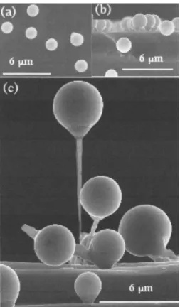
If a preexisting metal lies on the substrate, the cone base may be taller. Examples of such 3D-Ss are shown in Figs. 3–5 which present balloons, nanowires, or scepters. They are not sensitive to gravity; they grow vertically on top of the sub-strate or horizontally on its sides, demonstrating the strength of the bonds between the substrate and the carbon base.
In Fig. 3共b兲, the substrate is bare, no metal acting as a catalyst being present as in the VLS model; the 3D structure
looks like a montgolfier or balloon so共a兲 and 共b兲 are called “montgolfiers.”9–11,40In Fig. 3共c兲, the substrate is aluminum film/silicon; here also, no metallic cluster is acting as a cata-lyst; it shows scepterlike structures deposited by MOCVD on aluminum stripes. A carbon tube supports a much taller bal-loon. In the same way, Cu, Pt, Au, or In may be used as substrates; 3D-Ss are built through their interaction with or-ganometallic molecules.
Figures 4共a兲 and 4共b兲 depict nanowires made of
GaCuO2, on ⬃3.6 eV band-gap semiconductor, created by
the interaction of TMGa with a Cu substrate at 923 K.41As
described in Ref. 41, oxygen comes from the surface of the copper oxide substrate.
Figure 4 and Ref. 41 show clearly that many types of curved or nearly flat interfaces exist between the metallic cluster and the column for the construction of these 3D-Ss. The same results hold for the GalnP bamboo shaped structure shown in Fig. 5, created by the interaction of TMGa with an InP substrate.11,42
Keeping in mind these results, we present below some important points about the curvature or size effect already presented in the literature but adapted here to nanocolumn aspects and most common catalyst metals utilized by most in the PVD and CVD crystal growers community.
IV. THE SIZE/SHAPE CLUSTER-COOKING MACHINE
The bulk melting temperature TBof a material intervenes
in various technological fields, in particular, metallurgy of FIG. 3. MOCVD growth of 3D-S at 650 ° C. 共a兲 Top view of gallium spheres surrounded by a carbon envelope.共b兲 Side view of spheres lying on a carbon cone. The contrast allowed by SEM shows clearly the composi-tional difference between spheres and cones.共c兲 Scepter structure: a long and empty carbon structure capped by a Ga sphere covered with a thin 共10–25 nm兲 amorphous carbon membrane. The substrate is 共100兲 Si photo-lithographically prepared with 1 – 10m width and 100 nm thick Al stripes.
most common metals and alloys such as gold, aluminum, iron, copper, stainless steel, etc. These materials are pro-duced in large dimensions from millimeter to meter sizes and
over but some are made of aggregated grains 共micrometer
size兲. When the grain size decreases down to the nanometer
range, so does the melting temperature Tm that noticeably
deviates from TB共Refs. 17–19兲 beginning at a few
microme-ters. This phenomenon is not widely known; many but not all of its aspects are now understood; apart from sintering, we are not aware of applications to modern material production. Modern microelectronic and optoelectronic industries use ul-trapure metals and their alloys: Au, Al, In, W, Ti, Ni, Ag, Cu, Zn, Pt, Nb, etc. The use of metals of high purity and of nanosized dimensions open insights into other properties. When a cluster, aggregate of atoms, is a few nanometers in size, size effect appears as a phenomenon associated with curvature effect, and atoms do not behave anymore as in bulk material. This curvature effect leads to the bending of chains of atoms and a decrease of the strength of atom bond, as depicted by Fig. 6, that presents two bent chains of atoms
to exemplify this effect. Experimental results have shown that surface atoms of a cluster are more exposed to this cur-vature effect.
Melting comes from the influence of surface atoms on the volume. In other words, there is a competition between Gibbs free energies of surface and inner atoms of the cluster. Semenchenko’s model is among the simplest giving a varia-tion of the melting point with size. Input parameters are the latent heat L of melting, the diameter d of the metallic spherical particle, its bulk melting point TB, the interfacial
tension ␥ls between the solid and the liquid phase of the
material under study, and the density . It gives Tm共d兲
= TBexp共−4␥sl/Ld兲. 43
More elaborated models, which differ by the description and interpretation of melting, have been devised but, what-ever they are, at first order, Tm共d兲/TB⬃1−A/d, where A
en-closes ␥ls and L.17,44 The numerical values obtained with
various models are relatively close; so Semenchenko’s rela-tion is sufficient. When clusters have a low number of atoms,
A / d approaches 1 and melting is not very clearly defined.
Solid-liquid phase fluctuations occur45,46and Tmis no longer
a continuous function of the number of atoms.47
As an example, a high Tmmaterial such as gold melts at
1336 K and Tm共d兲 follows the behavior shown in Ref. 17.
One can see that a 1 nm diameter spherical Au cluster
con-tains ⬃25 atom melts below 300 K. Bulk gallium which is
the␣phase of Ga, a low Tmmaterial, melts at 302.9 K. Once
divided into small droplets, Ga is quite special because it no
longer exhibits its bulk ␣ phase but other crystallographic
phases, , ␥,␦, and with different melting temperatures,
for example, TB 共Ga兲=256.85 K and TB 共Ga␦兲
= 253.75 K. Figure 7 shows the behavior of the Gaand Ga
␦ phases as a function of d. A 1 nm diameter spherical
clus-ter contains⬃31 atoms and melts below 170 K. The melting
temperatures Tm共d兲 of high TB materials such as Fe and Ni
follow the same behavior as that of Au described in Ref. 17. This demonstrates that the size of the top cluster may influ-ence its state, solid or liquid, according to the temperature of the growth process and so is able to modify the 3D-S growth conditions.
Melting begins at places on the surface where the local radius of curvature is the smallest; a solid-liquid equilibrium exists over a few degrees before the end of melting being reached.23 Curvature effects exist for rounded or spherical surfaces; they obviously exist also for other shapes such as FIG. 4. GaCuO2 single nanowires grown on Cu substrates by MOCVD
共Ref. 38兲 as seen by HRTEM: 共a兲 rounded interface between the column and the cluster and共b兲 interstitial planes of a single crystal inside the column and bowed cluster/column interface.
FIG. 5. HRTEM picture of a GaInP nanowire obtained by MOCVD, created by the interaction of TMGa with an InP substrate held at 650 ° C共Ref. 39兲. The nanowire rod region is composed of GaInP disks rotated by 60 ° from each other.
FIG. 6. Two bent chains of atoms showing schematically that surface atoms are more weakly bound to their neighbors than the inner ones. Rcis the
grain corners or edges.48,49Figures 8 and 9 show dark field TEM pictures of Pb clusters around 561 K共TB= 600.56 K兲18
and Ga at 250 K for small size and deformed shape clusters, respectively.19,50
Note that, in Figs. 8 and 9, a big and a small sphere that coalesce create a nonspherical particle, for which melting begins at places where the radius of curvature is the smallest and at a temperature lower than that of the bigger sphere. Nature has gifted us with this phenomenon even for micrometer-size metallic growth. Facing these arguments and facts with the present science of nano- and microcrystal growth, we should be able to introduce different concepts. These concepts will be mentioned for atom by atom growth, growth of dots by solidifying melted metallic clusters, and nanocolumn growth.
V. IMPROVEMENT OF THE VLS GROWTH MODEL
We have shown that the VLS model in its present state is to be questioned and a more refined explanation should be found if one wants to explain the unusual structures exhib-ited by Fig. 3 and particularly the 3D scepters关Figs. 3共b兲 and 3共c兲兴.
Let us recall the geometric description as shown by the various samples. Seen from the top, the 3D-Ss look like spheres关Fig. 3共a兲兴; the side view shows that they are actually made of spheres supported by a cone, whose area in contact with the substrate is fairly small, diameter less than 10 nm. The top ball is a sphere to a very good accuracy. Its diameter
parallel to the substrate is ⬃2m while the top to bottom
distance is⬃2.35m关Fig. 3共b兲兴. The height of the cone is
⬃0.428m; its diameter measured at the interface between
the bottom of the cone and the ball is ⬃1m; this
corre-sponds to a⬃45° half-angle at the summit. The ball and its
associated supporting cone are attached to the substrate by an
empty column共a carbon tube兲 whose diameter is at least one
order of magnitude less that the ball’s diameter 关Fig. 3共c兲兴. For such scepter shown in Fig. 3共c兲, the diameters of the ball
and the column 共tube兲 are 3.69 and 0.13m, respectively;
the column length is 9.40m. The half-angle of the cone is ⬃40° and the ball-cone contact angle is ⬃138°. At the be-ginning of the growth process, the growing sphere presents a
flat interface with the thick and flat substrate. During the
column growth, this interface 共ball/column兲 may no longer
remain flat as it appears in Fig. 4.
Chemical and structural analyses of these 3D-Ss, per-formed using SEM, EDX, and TEM, have shown that the ball is mainly composed of liquid gallium, the cone being made of carbon for which more details are found in Refs. 10 and 51. If the ball-cone interface was to be flat, the Ga–C contact angle calculated from the geometry of the system
would be ⬃125°. This is in good agreement with previous
measurements of wetting angles of very high purity Ga on clean Al2O3single crystal; Ga exhibits a contact angle in the range of 118°–130°, that usually decreases if few metallic impurities are present on the substrate.52,53
The questions are as follows: How does the growth pro-cess start? What can be the driving forces 共catalysis, diffu-FIG. 7. Melting temperature Tmof Gaand Ga␦clusters as a function of
their diameter d: TBGa= 256.85 K and TBGa␦= 253.75 K.
FIG. 8. Dark field transmission electron microscopy共DFTEM兲 of spherical and nonspherical lead particles embedded in a SiO matrix, TB= 600.5 K,
taken from Ref. 23. Black areas C and D are associated with solid parts, bright ones are associated with solid parts in Bragg conditions for the elec-tron beam, and areas of intermediate gray levels represent elecelec-trons scat-tered incoherently by the liquid parts of the particles.
sion, segregation, etc.兲 building the whole 3D-S shown in
Fig. 3 共ball, cone, and tube兲? They are discussed in what
follows.
VI. HOW DOES THE GROWTH PROCESS START?
Generally, one can distinguish between Volmer-Weber54
and Frank–van der Merve55 growth modes; in between is
Stransky-Krastanov’s mode, a mixture of both the previous ones; one atom is the elemental brick. The way these atoms realize three-dimensional clusters, islands, or continuous films, amorphous or crystalline structures, depends on pa-rameters related to the material under growth, its substrate, and the experimental conditions of the growth itself. Experi-mental conditions such as patterning etching, chemical syn-thesis, stress driven organization, growth temperature, etc., are different. In what follows, but not relevant on the process itself, we examine how the presence or absence of a metallic cluster with its associated size effect may affect growth pro-cesses.
A. Atom by atom crystal growth
Currently, most of nanosized single crystal growers
uti-lize PVD and CVD methods such as MBE,33 CBE,5,6
LCG,2–4 MOCVD,8–11,34 metal-organic vapor phase epitaxy
共MOVPE兲,35
and atomic layer epitaxy共ALE兲 or atomic layer
deposition 共ALD兲.56 In these various methods, a spatially
continuous film crystal growth reduces to an atom by atom building process of its structure; atoms or molecules reach the substrate as individuals or partly cracked entities, orga-nize themselves, and form the crystal layer by layer. During
the first steps 共a few atoms兲 of the formation of a growing
cluster, temperature plays a role. Due to its size, the growing cluster is deeply into the conditions presented in Figs. 7–9; it experiences the thermodynamic size effect and its growth takes place in the liquid state. For most of PVD/CVD meth-ods, growth nutrients are in the condition where the vapor-liquid-solid mechanism holds, As an example, MOCVD or MBE growth of GaAs.34–36Cracking of nutrients for epilayer
growth needs relatively high temperatures 共800
– 1000 K兲;7–10,35
on the contrary, thermal requirements are much lower in liquid solutions, down to 400 K and below,
and VLS or SLS mechanisms hold in the same way.14–16
Achievement of lower thermal requirements is then obtained using a small liquid metallic cluster whose melting tempera-ture has been lowered, thanks to the size effect. Of course, as size increases and reaches the micrometer range, the influ-ence of the thermodynamic size effect on the metallic cluster, and so on the growth conditions, decreases strongly and dis-appears.
B. Nanocolumn growth assisted by a metallic cluster
We have shown in Sec. II that the VLS growth mecha-nism suffers actually from unresolved questions that can find their origin in size effects as described above. The VLS model, accepted as it is, imposes a metallic ring, limiting a meniscus, on top of the growing column and between the flat-rounded regions. The radius of curvature of this ring is in the range where size effects cannot be neglected. Moreover, catalysis takes place on the whole surface of the metallic cluster, a process that releases heat. In the vicinity of the ring, exothermic catalysis should be more active than else-where because species cracked there are used for building the column; then more heat should be released close to the ring; its temperature is higher than in other places on the metallic cluster surface and the rest of the column. The tem-perature of the ring is then higher than the melting one of, for
example, if used, a 10 nm diameter gold cluster.17 A gold
cluster may exhibit solid zones associated with low curva-tures and liquid zones associated with high curvacurva-tures for which the size effect applies.
How can one reconcile rounded and flat cluster/column interfaces? At the beginning of the growth process, the clus-ter lies on the substrate and the contact zone reproduces its curvature, in our case a flat interface. As soon as growth begins in the region located between the cluster and the sub-strate, interfacial tensions appear and the associated forces determine the external shape of the cluster as well as the curvature of the interface. The cluster remains on top of the growing column and their interface may be bended, depend-ing on the various forces that are exerted on both materials on each side. Then, if a flat cluster/column interface is to appear after the growth, it must be due to the subsequent step related to the column formation or evolution. Arguments based on these facts do not evacuate the physical problem. Now, surface tension and interfacial tensions that govern, respectively, the shape of the metallic cluster and the con-vexity of the cluster/column interface may be not strong enough to create a visible bending. Unfortunately, HRTEM pictures are obtained after growth has stopped; relaxation processes may have taken place leading to flat interfaces. This does not prevent curved interfaces from existing: the visible curvature is created by couples of materials in con-tact, such as cluster/growing column, for which the ratio of interfacial forces to Young modulus enables such a visible bending to occur. This may explain why various convexities of cluster/growing column interfaces are found,41depending on such couples of materials 共Fig. 4兲.
FIG. 9. DFTEM of spherical and nonspherical gallium particles embedded in a SiOxmatrix, taken from Ref. 50.
In this way, the VLS model by Wagner and Ellis still holds, although it has to be modified taking into account the following points.
共a兲 A metallic cluster and its surface atoms exhibit, respec-tively, curvature effects and diffusion process.
共b兲 The different materials build the column following the general lines described above: curvature effects added to diffusion processes, etc.
共c兲 The surface of the cluster plays a twofold role: cataly-sis and surface diffusion of cracked species toward the growing zone. The last point, diffusion, is the most important step and is described in more detail below. Mainly, the growth mechanism by diffusion of nutri-ents through the cluster has to be replaced by a surface controlled growth mechanism, as recently proposed in the case of nanowires and nanotrees.28
Suggestions and arguments for a more acceptable model are developed in the next paragraphs.
Arguments for a surface diffusion model
We have seen that a more convenient model of cluster/ column growth has to be set up. The metallic cluster, the cooking machine, acts as a catalyst; its surface or part of it may be in the solid or liquid state.17The nutrients cracked at their surface are supposed to travel through the cluster to-ward the growing zone, namely, the cluster/column interface, and create the 3D-S共Fig. 2兲.12We bring arguments in favor of surface diffusion as proposed in Ref. 28.
The temperature of the growth process and the small size of the metallic cluster act in the same direction: the melting temperature of curved zones decreases and the smaller the curvature, the bigger this decrease.17 Near the contact zone of the cluster on the growing column, the cluster exhibits the highest curvature; this ring may be liquid while the rest of the cluster is in the solid state. However, for the sake of clarity, we will not go into such details and will keep a given state for the cluster.
If solid, most of the time, small metallic clusters are single crystals. Gold particles exhibit compact共111兲 surfaces whose surface tension is minimum; they appear as practi-cally spherical under TEM for sizes lower than 10 nm
diameter.17 High-resolution electron microscopy of Pb
par-ticles reveals the existence of facets and also rapid changes of the orientation of the crystallographic structure, even at
temperatures lower than Tm. Although the cluster does not
rotate as a whole, the orientations of its atomic planes are changing all the time, as demonstrated in Ref. 50. In such a case, it is difficult to understand how atoms diffuse through an evolving crystalline structure and reach the growing inter-face. As a matter of fact, the atoms of nutrients that build the column and have reacted at the surface of the cluster would have to channel through its moving atomic planes and keep the direction of the growing interface without having any
driving force to go to the considered interface 共cluster/
column兲. Whatever the diffusion model used 共interstitial, substitution, etc.兲, the atoms diffusing inside the cluster will be guided by channeling processes and follow their initial
diffusion direction; it is very unlikely that this direction co-incides with that of the cluster/column interface.
If the cluster is liquid, crystallographic planes are smeared out and atoms are subjected to Brownian motion; the arguments against diffusion through the volume remain valid. Interactions of a given species of atoms with those of the cluster do change at its melting; however, this change is not so abrupt compared to that of other physical parameters such as electrical resistivity. Above melting, the surface is
“more liquid” than the volume共Figs. 8 and 9兲. Simulations
show that atoms move on the surface more than inside where the interaction with others remains uniform as an average, not giving rise to a driving force.57
Previous high-resolution electron microscopy experi-ments have shown that a gold single crystal experiences evaporation condensation at the atomic scale as well as dif-fusion of its surface atoms;58–60coalescence between crystal-line clusters also occurs from surface atoms and not from volume ones.61In this context, it is more likely that nutrient atoms cracked at the metallic cluster surface behave in the same manner: they diffuse along the outer surface of the cluster instead of penetrating it. This is to be related with a nowadays generally accepted view that, in MOVPE, decom-position of precursor materials happens to a large degree outside the cluster/wire structure. The vicinity of the surface cluster may play both roles: catalyst and collector of decom-position products.
So, whatever the states of the catalyst cluster are, what can be the origin of a force driving the nutrients to the grow-ing zone?
Let us show that this force is a consequence of the dif-fusion of nutrient atoms along the surface of the catalyst cluster and of the beginning of the growth process. Before growth starts, surface atoms of the metallic cluster itself are able to move on the surface, activated by thermal energy. Surface energy tends to a minimum and so, for a given num-ber of atoms, the free surface of the cluster takes roughly a spherical shape except at the contact zone with the substrate where it imposes its own shape. When nutrients are created at the surface, they experience Brownian motion and show instantaneous velocities with random directions but there is still an intrinsic probability that they establish chemical bonds. The existence of the ring, contact line between the cluster and its substrate, modifies the picture: part of the random character of velocities is lost. They must reverse their orientations and cross a null value, and then nutrient atoms that were neighbors when entering this zone spend more time close together than in other zones on the cluster surface. The probability that they establish bonds is in-creased there and will remain always higher than elsewhere: the growth process from nutrient atoms starts from the con-tact ring.
Once growth has started, it consumes nutrient atoms; the growing zone共the cluster/column interface兲 exhibits a lower concentration of free nutrients than the rest of the cluster surface. Then, a gradient of concentration exists along the cluster surface. Classically, a driving force is associated with this gradient and creates a flux of nutrients toward the ring and the growing zone, the metallic cluster/column interface.
Returning to the solid or liquid state of the catalyst clus-ter, the liquid cluster exhibits a truncated sphere shape lying on the interface with the growing column. Catalysis occurs on its surface; the diffusion coefficient of atoms on the sur-face of a liquid is higher than on or inside a solid. The gradient of nutrient concentration still exists but is higher for a liquid cluster than for a solid one, leading to a higher growth rate and efficiency of the process. If the catalyst clus-ter exhibits solid and liquid zones, the previous arguments remain valid.
Another argument for a surface diffusion assisted growth comes again from wetting or interfacial forces. When one considers a mixture of two different metals, at a temperature such as both are in the liquid state, it may exist as a domain of miscibility and wetting. Above some critical temperature, the metal with the lower interfacial energy segregates at the outside of the other one.62,63Such a segregation strongly re-duces the probability of finding atoms of the segregated metal below the few layers confined close to the exterior. It is possible to propose a volume diffusion of C inside the liquid Ga cluster toward the interface? It requires that some miscibility domain or compound between carbon and gal-lium exist. We are not aware of any C–Ga phase diagram nor GaC carbide. Experiments done on carbon nanotubes filled by Ga and exposed to temperature higher than 700 K do not
show the formation of a Ga–C compound.64,65Moreover, in
the experiments reported here, because of the low tempera-ture, and although C atoms are not equivalent to metallic ones, they cannot be considered as in a “liquid state.” As a consequence, C should not penetrate the liquid metallic clus-ter over a few layers; a dewetting should occur between liq-uid Ga and “solid” carbon, favoring a surface diffusion pro-cess. Once a thin layer of C atoms covers a Ga droplet, although temperature is not comparable, the experimental situation is similar to that of liquid Ga in contact with dia-mond. In this case, it has been shown that the liquid layers of Ga in close contact with diamond experience an ordering and assume a solidlike structure that should influence its
hetero-geneous nucleation.66 Then, at low temperature, Ga should
nucleate and freeze. In our case 共Figs. 3–5兲, temperature is higher than the nucleation temperature of solid Ga and Ga remains liquid, but nothing prevents C atoms on the surface
from organizing themselves,67 helped by the underlying
or-ganization of liquid Ga.
As a summary, temperature controls the solid or liquid state of the cluster, its chemical activity as a catalyst, the amplitude of characteristic parameters of surface diffusion, and the intrinsic probability of forming bonds. Surface dif-fusion controls both the external shape of the catalyst cluster even in the solid state and the growth process. The presence of the contact ring between the cluster and its substrate in-creases the probability of forming chemical bonds close to it; the concentration gradient of free nutrients as created gives rise to the driving force that leads atoms in the growing zone, the cluster/column interface.
C. MOCVD growth of 3D-S perpendicular to the substrate
As shown in Fig. 3共b兲, 3D-Ss grow up perpendicularly to
the surface of single crystal or amorphous flat
substrates.9–11,40 There is no relation of heteroepitaxy be-tween the crystalline state of the substrate and the 3D scepter structure composed of a carbon cone shaped base and a me-tallic sphere on top: the 3D-S does not copy the underlying crystallographic states.51This is not always the case; it may happen that a metallic epitaxial growth reproduces the under-lying structure of a crystalline substrate although separated from it by an amorphous and dielectric layer a few nanom-eter thick.66 However, even in this case, the epitaxy takes place perpendicularly to the substrate.
Defects, impurities, and steps are present on the sub-strate and are randomly distributed. During the MOCVD process, atoms diffuse on and above the substrate and are anchored by these defects/impurities and then a preferential growth of the catalyst cluster takes place at these points. The first step of growth occurs in the liquid state, because of the thermodynamic size effect, helped by the heating of the sub-strate; wetting conditions determine the characteristic shape of the truncated sphere of the clusters as demonstrated in Fig. 3.
A cone shaped carbon base, or carbon column, has been evidenced for these 3D-Ss; the first 3D-S seed comes very likely from a surface interaction between a carbon radical
and the substrate.51 The TMGa molecule gives the carbon
radical. The carbon base and sphere grow together. The con-tact zone between the conical carbon base and the gallium cluster can be seen as the cooking machine described above. The beginning of the seed formation is facilitated by the existence of the first Ga–C atoms that strongly experience the size effect because of the low content of Ga atoms. Dur-ing the MOCVD process, Ga and carbon keep beDur-ing fed to both cluster and cone, then the cone and the carbon mem-brane that surrounds the cluster have to grow or expand.
It is known that in comparable experimental situations,
carbon nanotubes grow perpendicularly to a Si共001兲/SiO2
substrate;68the growth mechanism is helped by the presence of metallic clusters that act as catalysts. The growth process of the column may start from the contact zone or ring: it forms a carbon cone and a metallic cluster detaches from the substrate. If no more nutrients are injected, nothing changes. If nutrients are injected by the CVD phase or from the sub-strate itself, then the carbon cone expands in a column关Figs. 3共b兲 and 3共c兲兴 from the ring, perpendicularly to the substrate. This is supported by experiments on the growth of multi-walled carbon nanotubes from a metallic cluster, for which a
proposed mechanism among others would be stresses.69
Then, two possibilities have to be considered: either the clus-ter remains on the substrate and the carbon column grows from the cluster and in the opposite direction to the substrate,69or the cluster is detached from the substrate. This last possibility is exemplified by multiwalled nanotubes that grow from a metallic Ni layer deposited onto Si共001兲/SiO2.
process.70Then, the column may grow in between the sub-strate and the metallic cluster共Figs. 4 and 5兲.
In the liquid state, more than in the solid state, the cluster/substrate catalyst couple exhibits an axis of symme-try, perpendicular to the substrate, and it remains unchanged under a rotation around it. At the beginning of the growth process, the probability that bonds form along the carbon cone/cluster interface is also isotropic compared to this axis. As a consequence, the 3D-S should grow perpendicular to the substrate and should keep this symmetry. This is what Fig. 3共b兲 shows. However, it is known that directions of growth other than perpendicular to the substrate can be real-ized and their origin may be found in some broken
symme-try, surface steps, and surface exposed alloys 关see some
3D-Ss in Figs. 3共b兲 and 3共c兲兴.
When metallic films are present on the substrate, they create preferential sites of nucleation for the catalyst clusters; they also constitute sources of atoms for alloying and rota-tional symmetry of the growth conditions may be broken. The direction of growth remains no longer perpendicular to the substrate and more complicated 3D-Ss can be obtained in these conditions关see Figs. 3共c兲, 4, and 5兴.9–11,40–42
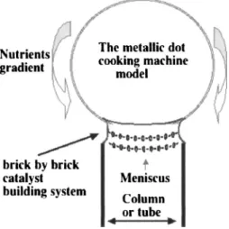
Keeping in mind the previous arguments and the experi-mental results that support them, we propose to improve the so-called VLS growth model according to a scheme de-scribed in Fig. 10.
A metallic cluster, or cooking machine, acts as a catalyst that feeds nutrients. Its surface or parts of it may be in the liquid state, due to the thermodynamic size effect added to the heat released from catalysis and heated substrate. Surface diffusion of nutrients helps building brick by brick 共atoms兲 the column. Minimization of the various surface energies governs the convexities of the various interfaces, cluster/ column and column/substrate; structural relations govern the structure of the growing column. An argument of this scheme uses the decrease of the melting temperature of a localized zone in the vicinity of the cluster/column interface, a zone which is responsible for the brick by brick construction of the structure.
The brick by brick construction of the single or multi-walled carbon tube can be regarded in the same model: the
physical state of the metallic cluster共entirely liquid or some part of its surface liquid and some solid兲 gives rise to the skeleton to be produced.
D. How to choose the metallic catalyst cluster
Although the answer to this question does not modify what has been presented before, such a choice governs the chemical reaction to be favored and the efficiency of the catalytic process. As an example, gold is preferred for the
growth of carbon nanotubes and III-V compounds.2–8Such a
choice presents many advantages: a very weak affinity to oxygen, a low vapor pressure up to Tm共no evaporation or an
extremely low one兲 during the experiment, and the remaining constant of the size of the cluster. In such a respect, Ga also presents a very low vapor pressure, remains liquid over an extended temperature range, and its cluster keeps a constant shape of truncated sphere whatever the conventional growth temperature is.
It shows that the nature of atoms is involved but not their physical state共liquid or solid兲. In this respect one can under-stand that the physical state共liquid or solid兲 of the metallic catalyst cluster is not so important for the catalysis process. Let us examine the influence of the size of the catalyst cluster. Let NS and NVbe, respectively, the number of atoms
located on the surface and the whole number of atoms in the cluster. Bulk material is characterized by NS/ NV⬇0, while it
is 1 for a single atom. A decrease of size is accompanied by an increase of NS/ NV. A spherical cluster of diameter d and a
cubic crystallographic structure with a lattice parameter b give NS/ NV= 3b / d; for example, a d = 3 mm lead cluster
gives NS/ NV⬃0.5. Gold has the same crystallographic
struc-ture as lead, although its lattice parameter is slightly differ-ent; its NS/ NV remains quite comparable to 0.5. Most of
at-oms from very small clusters are located at its surface, increasing the efficiency of the catalytic process.
VII. CONCLUSION
The growth of modern materials structures with three
dimensions 共nanowires, columns, balloons, scepters兲 has
been presented and discussed in relation to the melting tem-perature of nanosized metallic cluster acting as catalysts, which we call the cooking machine. The VLS growth mecha-nism proposed in the 1960s has been discussed and ap-proached to more recent growth descriptions of 3D-S mate-rials. Organometallic self-catalysts used for the construction of 3D-S materials have been incorporated into today’s infor-mation and literature on existing 3D-S. The currently ne-glected melting temperature of nanosized metallic materials has been applied to the known growth of 3D shape columnar materials. The melting temperature decreases with the size of the metallic particle. The shape of nanosized materials共as a consequence of the surface curvature effect兲 has also been related to existing growth in nanomaterials science. It seems that a surface driven 3D-S growth mechanism would be more appropriate than the initially proposed diffusion mechanism through the volume and would give a better in-sight into an actual VLS mechanism of 3D-S growth. The metallic cluster-cooking machine that has been presented, FIG. 10. Model of the construction of a column by a 3D-S metallic dot
discussed and extended to many existing growth techniques, can help in a future and more efficient description of a com-plete physical micro-/nanosized column growth mechanism. The size and shape of metallic cluster can be responsible for many and intriguing results related to 3D-S growth. Some aspects of many and not yet physically related facts such as twining and/or kinking through the growth direction of wires, single/multiwalled carbon tubes, cluster/wire flatness or curvature of interfaces, and tapering have been examined through size effects that a metallic cluster experiences. A few recent results about MOCVD, assisted growth of 3D-S orga-nometallic self-catalysts, have been presented and deal with the growth of metallic/carbon and metallic/semiconducting
structures. GaInP and GaCuO2 nanosized wires as well as
micrometer-sized GaN crystals have been obtained by the organometallic precursor interaction with many kinds of sub-strates. We hope that the chemical/physical description of MOCVD, curvature effects, and 3D-S shape, involved during growth phenomena, can help improve material research and present a more general mechanism in order to obtain nano-sized materials and devices for future developments. The present discussion can also be applied to devices such as GaInN quantum dots intended for visible laser materials. This information is presented as a challenge to be overcome and not as an end. Nevertheless, considerable information is still needed to build a complete scientific explanation of the wonderful and exciting nanoscience world of dots, wires, and single or multiwalled tubes.
ACKNOWLEDGMENTS
This work is part of the FILEMON35 project. We ac-knowledge the financial support of the “Agence Nationale de la Recherche” under Contract No. ANR-05-NANO-016-04.
1S. Iijima, Nature共London兲 354, 56 共1991兲.
2J. Wang, M. Gudiksen, X. Duan, Y. Cui, and Ch. Lieber, Science 293,
1455共2001兲.
3M. Gudisksen and Ch. Lieber, J. Am. Chem. Soc. 122, 8801共2000兲. 4X. Duan and Ch. Lieber, Adv. Mater.共Weinheim, Ger.兲 12, 298 共2000兲; J.
Am. Chem. Soc. 122, 188共2000兲.
5B. Ohlsson, M. Bjork, M. Magnusson, K. Deppert, L. Samuelson, and L.
Wallenberg, Appl. Phys. Lett. 79, 3335共2001兲.
6U. Krishnamachari, M. Borgstrom, B. Ohlsson, N. Panev, L. Samuelson,
W. Seifert, M. Larsson, and L. Wallenberg, Appl. Phys. Lett. 85, 2077 共2004兲.
7J. Motohisa, J. Noborisaka, J. Takeda, M. Inari, and T. Fukui, J. Cryst.
Growth 272, 180共2004兲.
8K. Hiruma, M. Yazawa, T. Katsuyama, K. Ogawa, K. Haraguchi, M.
Koguchi, and H. Kakibayashi, J. Appl. Phys. 77, 447共1995兲.
9M. Sacilotti, L. Imhoff, S. Bourgeois, C. Dumas, J. Decobert, P. Baldeck,
and I. Colombier, J. Cryst. Growth 261, 253共2004兲.
10M. Sacilotti, L. Imhoff, C. Dumas, J. C. Vial, P. Baldeck, I. Colombier,
and F. Donatini, Jpn. J. Appl. Phys., Part 2 43, L698共2004兲.
11M. Sacilotti, J. Decobert, H. Sik, G. Post, C. Dumas, P. Viste, and G.
Patriarche, J. Cryst. Growth 272, 198共2004兲.
12R. Wagner and W. Ellis, Appl. Phys. Lett. 4, 89共1964兲. 13E. Givargizov, J. Cryst. Growth 20, 217共1973兲; 31, 20 共1975兲. 14T. Trentler, K. Hickman, S. Goel, A. Viano, P. Gibbsons, and W. Buhro,
Science 270, 1791共1995兲.
15H. Yu, P. Guibbons, K. Kelton, and W. Buhro, J. Am. Chem. Soc. 23,
9198共2001兲.
16H. Yu, J. Li, R. Loomis, L. Wang, and W. Buhro, Nature共London兲 2, 517
共2003兲.
17Ph. Buffat and J. P. Borel, Phys. Rev. A 13, 2287共1976兲.
18P. Cheyssac, R. Kofman, G. Mattei, P. Merli, A. Migliori, and A. Stella,
Superlattices Microstruct. 17, 47共1995兲.
19R. Kofman, P. Cheyssac, Y. Lereah, and A. Stella, Eur. Phys. J. D 9, 441
共1999兲.
20M. Bjork et al., Nano Lett. 2, 87共2002兲.
21A. Persson, B. Ohlsson, S. Jeppesen, L. Jensen, and L. Samuelson, J.
Cryst. Growth 272, 167共2004兲.
22R. Kofman, P. Cheyssac, A. Aouaj, Y. Lereah, G. Deutscher, T.
Ben-David, J. Penisson, and A. Bourret, Surf. Sci. 303, 231共1994兲.
23P. Cheyssac, R. Kofman, and A. Aouaj, in Physics and Chemistry of Finite
Systems: From Clusters to Crystals Vol. 1, NATO Advanced Studies In-stitute, edited by P. Jena, S. N. Khanna, and B. K. Rao共Kluwer Academic, Dordrecht, 1992兲, Vol. 1, pp. 387–392.
24M. Pinault, V. Pichot, H. Khodja, P. Launois, C. Reynaud, and M.
L’Hermite, Nano Lett. 5, 2394共2005兲.
25S. Lee, N. Wang, and C. Lee, Mater. Sci. Eng., A 286, 16共2000兲. 26W. Shi, Y. Zheng, N. Wang, C. Lee, and S. Lee, Adv. Mater.共Weinheim,
Ger.兲 13, 591 共2001兲.
27Czochralski method, Ref. 20 of W. Runyan, Silicon Semiconductor
Tech-nology共McGraw-Hill, New York, 1965兲, pp. 38–49.
28A. Dick, K. Deppert, M. Larsson, W. Seifert, L. Wallenberg, and L.
Sam-uelson, J. Cryst. Growth 272, 131共2004兲.
29J.-J. Métois, Surf. Sci. 241, 279共1991兲. 30M. Kern, Surf. Sci. 264, 467共1992兲.
31J. Olives Banos, J. Phys.: Condens. Matter 5, 2081共1993兲. 32P. G. De Gennes, Rev. Mod. Phys. 57, 827共1985兲.
33E. Søndergaard, R. Kofman, P. Cheyssac, F. Célestini, T. Ben-David, and
Y. Lereah, Surf. Sci. 388, L1115共1997兲.
34H. Manasevit, J. Cryst. Growth 55, 1共1981兲.
35J. Nishizawa, H. Sakuraba, and T. Kurabauashi, J. Vac. Sci. Technol. B 14, 136共1996兲.
36O. Bord, R. Talalev, S. Karpov, and Y. Makarov, Phys. Status Solidi A 176, 297共1999兲.
37J. Yu, E. Wang, J. Ahn, S. Yoon, Q. Zhang, and M. Yu, J. Appl. Phys. 87,
4022共2000兲.
38Y. Chen, J. Fitz Gerald, L. Chadderton, and L. Chaffron, J. Metastable
Nanocryst. Mater. 2–6, 375共1999兲.
39Y. Chen, J. Fitz Gerald, L. Chadderton, and L. Chaffron, Appl. Phys. Lett. 74, 2782共1999兲.
40L. Imhoff, M. Sacilotti, C. Josse Courty, M. Mesnier, M. C. de Lucas, and
S. Bourgeois, Phys. Status Solidi C 1, 388共2004兲.
41Th. Chiaramonte, G. Patriarche, J. Decobert, L. P. Cardoso, and M.
Sacil-otti, Nanotechnology 16, 2790共2005兲.
42M. K. K. Nakaema, M. P. F. Godoy, M. J. S. P. Brasil, F. Iikawa, D. Silva,
M. Sacilotti, J. Decobert, and G. Patriarche, J. Appl. Phys. 98, 535共2005兲.
43V. K. Semenchenko, Surface Phenomena in Metals and Alloys共Pergamon,
New York, 1961兲.
44P. Cheyssac, M. Geddo, R. Kofman, P. G. Merli, A. Migliori, A. Stella,
and P. Tognini, Mater. Sci. Forum 195, 161共1995兲.
45P. Cheyssac, R. Kofman, P. G. Merli, A. Migliori, and A. Stella, Mater.
Res. Soc. Symp. Proc. 332, 108共1994兲.
46A. Stella, A. Migliori, P. Cheyssac, and R. Kofman, Europhys. Lett. 26,
265共1994兲.
47R. Kusche, Th. Hippler, M. Schmidt, B. von Issendorff, and H. Haberland,
Eur. Phys. J. D 9, 1共1999兲.
48T. Nguyen, P. S. Ho, T. Kwok, C. Nitta, and S. Yip, Phys. Rev. Lett. 57,
1919共1986兲.
49J. Q. Broughton and G. H. Gilmer, Phys. Rev. Lett. 56, 2692共1986兲. 50Y. Lereah, R. Kofman, J. M. Penisson, G. Deutscher, P. Cheyssac, T. Ben
David, and A. Bourret, Philos. Mag. B 81, 1801共2001兲.
51P. Viste et al., J. Cryst. Growth 272, 466共2004兲.
52D. Chatain, I. Rivollet, and N. Eustathopoulos, J. Chim. Phys.
Phys.-Chim. Biol. 84, 201共1987兲.
53D. Chatain, I. Rivollet, and N. Eustathopoulos, Rev. Phys. Appl. 23, 1055
共1988兲.
54M. Volmer and A. Weber, Z. Phys. Chem., Stoechiom. Verwandtschaftsl. 119, 277共1926兲.
55F. C. Frank and J. H. van der Merve, Proc. Roy. Soc. 198, 216共1949兲. 56M. Leskela and M. Ritala, Angew. Chem., Int. Ed. 42, 5548共2003兲. 57T. Nissila, R. Ferrandos, and S. Ying, Adv. Phys. 51, 949共2002兲. 58L. D. Marks and D. J. Smith, Nature共London兲 303, 316 共1983兲. 59J. O. Bovin, R. Wallenberg, and D. J. Smith, Nature共London兲 317, 47
60Nature共London兲 315, 628 共1985兲.
61M. Flüeli, P. A. Buffat, and J. P. Borel, Inst. Phys. Conf. Ser. 8, 311
共1988兲.
62N. Lei, Z. Huang, and S. A. Rice, J. Chem. Phys. 107, 4051共1997兲. 63A. H. Ayyad and W. Freyland, Surf. Sci. 506, 1共2002兲.
64Y. Gao, Y. Bando, Z. Liu, and D. Golberg, Appl. Phys. Lett. 83, 2913
共2003兲.
65Y. Gao and Y. Bando, Appl. Phys. Lett. 81, 3966共2002兲.
66W. J. Huisman, J. F. Peters, M. J. Zwanenburg, S. A. deVries, T. E. Derry,
D. Abernathy, and J. F. van der Veen, Nature共London兲 390, 379 共1997兲.
67R. W. Cahn, Nature共London兲 375, 363 共1995兲.
68B. Q. Wei, Z. J. Zhang, P. M. Ajayan, and G. Ramanath, Carbon 40, 47
共2002兲.
69C. J. Lee and J. Park, Appl. Phys. Lett. 77, 3397共2000兲.
70B. Q. Wei, Z. J. Zhang, G. Ramanath, and P. M. Ajayan, Appl. Phys. Lett. 77, 2985共2000兲.


![Band offsets of n-type electron-selective contacts on cuprous oxide (Cu[subscript 2]O) for photovoltaics](data:image/gif;base64,R0lGODlhAQABAIAAAP///wAAACH5BAEAAAAALAAAAAABAAEAAAICRAEAOw==)