A Clock-Based Analog Memory Element for Integrated Circuits
by
Micah G. O'Halloran
B.S., Electrical and Computer Engineering (2000) University of Florida
Submitted to the Department of Electrical Engineering and Computer Science in Partial Fulfillment of the Requirements for the Degree of
Master of Science in Electrical Engineering at the
Massachusetts Institute of Technology September 2002
@ 2002 Massachusetts Institute of Technology All rights reserved
BARKER MASSACHUSETS INSTITUTE OF TECHNOLOGY
NOV 1 8 2002
LIBRARIES Signature of Author...Department of Electrical Engineering and Computer Science July 31, 2002
C ertified by... Assistant Professor
Rahul Sarpeshkar of Electrical Engineering and Computer Science Thesis Supervisor
7
A ccepted by...
Arthur C. mith Chairman, Department Committee on Graduate Students Department of Electrical Engineering and Computer Science
A Clock-Based Analog Memory Element for Integrated Circuits
by
Micah G. O'Halloran
Submitted to the Department of Electrical Engineering and Computer Science On August 9, 2002 in Partial Fulfillment of the
Requirements for the Degree of Master of Science in Electrical Engineering
ABSTRACT
A clock-based signal restoration scheme was developed as a method of implementing an analog memory cell for integrated circuits (ICs). The technique is similar to single-slope analog-to-digital (A/D) conversion, however, since the goal of the memory is to store an analog, rather than digital voltage, the digital memory circuits and the digital-to-analog (D/A) conversion circuits are not needed. An analog memory cell implementing this clock-based signal restoration algorithm was designed and fabricated using the MOSIS AMI 1.5pm CMOS process.
Experimental results show that the memory element possesses 8-bits of resolution from input to output, with a 2.8V input range when powered from a 3.3V rail. The experiments also show that the memory element is capable of storing an analog value with 8-bits of precision for over 2.5 hours. Storage at 8-bits of precision for indefinite lengths of time should be possible with the addition of more stable on-chip biasing circuitry and the use of better power-supply-rejection techniques in the ramp generator construction. The fabricated memory cell size on the AMI 1.5pirm process is 300plm x 250pam (375X x 310k).
Thesis Supervisor: Rahul Sarpeshkar
Table of Figures
Figure 1.1-- Capacitive storage is the simplest form of analog storage. In this technique, a MOS transistor is used as a switching element to connect and disconnect the signal source Vin from the capacitor Csamp. The value of ViM at the time the transistor tums off is held on C sam p... 11
Figure 1.2- A possible way of implementing low-leakage capacitive storage with contstant charge injection. In this circuit, the input voltage Vin drives the negative terminal of the left op-amp. When the transistor is switched on, the output voltage of the second op-amp must integrate current on Csamp until the voltage on Csamp is equal to Vi. Notice that after the circuit settles, both the source and drain of the switching transistor are at ground, because of the virtual ground established by the second op-amp at this node. The charge injection AQ is still nonzero in this circuit, however it is now a constant value independent of the value of Vin. ... ... .... . . 14
Figure 1.3-- Overview of floating-gate transistor operation. Two different mechanisms are typically used to transfer charge onto and off of a floating gate. Hot-electron injection occurs when electrons are accelerated to such a high speed at the drain of a transistor that they can pass through the gate oxide energy barrier and enter the floating gate. Tunneling occurs when a large positive voltage difference is created
between the Vtn terminal and the control gate, causing electrons to tunnel from the
floating gate through the thin gate oxide to the n- region. The disadvantage of these techniques is that they require large voltages to establish reasonable current levels, gate oxide trapping slowly degrades the efficiency of current injection as the cell is exercised, and the current levels are ill-defined, requiring special tuning methods to achieve high-resolution floating gate voltages. ... 15
Figure 1.4-- A floating-gate NMOS transistor and a PMOS current source are used to create a common-source amplifier, with Chold in the feedback path. A simple representation of the circuit is shown on the right. Through the impedance divider
formed by Chold and Cpar, the input voltage is pegged. Any charge added or removed from the input floating node is immediately counteracted by a movement of the output of the amp. Thus, this structure acts as an analog storage cell capable of driv in g lo ad s... 16 Figure 1.5- This figure shows a top-level view of an analog-to-digital-to-analog (A/D/A)
converter. The converter takes in an analog signal, creates a digital representation of it using an analog-to-digital (A/D) converter, stores the digital representation in digital flip-flops, and re-creates a quantized version of the original signal using a
digital-to-analog (D /A ) converter. ... 18 Figure 1.6- (a) The analog circuitry required for implementing Hochet's
quantized-analog memory. (b) Typical waveforms from the circuit's operation... 20 Figure 1.7- Cauwenbergh's partial-refresh oversampling analog memory cell... 23 Figure 2.1- (a) System-level view of the circuitry needed to implement the chosen
algorithm. (b) Typical waveforms present during the operation of the circuit in (a). ... 2 9 Figure 2.2- Magnified view Of Vramp and VCstore signal behavior during the critical portion of the restoration cycle... 31
Figure 2.3 - A full V2 bit of charge leakage off of the capacitor can be counteracted with the quantized analog storage technique. ... 31 Figure 2.4 - A full % bit of charge leakage onto the capacitor can be counteracted with
the quantized analog storage technique. ... 32 Figure 2.5 - This figure illustrates how a full bit of quantization error can occur when a
new value is stored in the m em ory cell... 33 Figure 3.1 - NMOS transistor symbol labeled with the voltage and current variables
typically used in describing its operation... 37 Figure 3.2 - ID versus VDS for different values of VGS. This data was simulated in SPICE
based on models from the MOSIS 1.5 jm CMOS process that will be used for
fabricating the m em ory cell. ... 37 Figure 3.3 - Small signal model of a MOSFET transistor operating in the triode region.39 Figure 3.4 - Small signal model of a MOSFET transistor operating in the saturation
reg io n . ... 4 0 Figure 3.5 - PMOS input common-source amplifier circuit (left) and the symbol used to
represent it (right). ... 43 Figure 3.6 - Simplified small-signal model of PMOS-input common-source amplifier. 44 Figure 3.7 - Bode plot of the transfer function of the common-source amplifier shown in
Figure 3.5, with the NMOS transistor biased to supply 1 pA. ... 47 Figure 3.8 - Noise model for the common-source amplifier... 48 Figure 3.9 - SPICE simulated input-referred noise spectral density for the PMOS-input
common-source amplifier biased at ID =1A. ... 49 Figure 3.10 -- NMOS input common-source amplifier circuit (left) and the symbol used
to represent it (right). ... 50
Figure 3.11 -- Bode plot of the transfer function of the common-source amplifier shown in Figure 3.10, with the PMOS transistor biased to supply IpA... 51
Figure 3.12 -- SPICE simulated input-referred noise spectral density for the NMOS-input common-source amplifier biased at ID = 1 iA. ... 52
Figure 3.13 - PMOS-input operational transconductance amplifier (P-OTA) circuit (left) and the symbol used to represent it (right)... 53 Figure 3.14 - Small-signal behavior of OTA currents given a small-signal voltage input.
... 5 5 Figure 3.15 - PMOS transistor with bootstrapped well to reduce parasitic junction
leakage w hile the transistor is off. ... 57
Figure 3.16 - Block diagram of an OTA in unity negative feedback (a), and a reduced block diagram of the sam e system (b). ... 58 Figure 3.17 - Response of a single-pole transfer function to a ramp input. The first term
in the output would be the response of an amplifier with no dynamics. The second term in the output settles to a constant error term in steady state... 59 Figure 3.18 -- Bode plot of the transfer function of the P-OTA shown in Figure 3.13,
b iased at 1 A . ... 6 3 Figure 3.19 -- SPICE simulated input-referred noise spectral density for the PMOS-input
O TA biased at ID = A . ... 64
Figure 3.20 - Transmission gate circuit (left) and the symbol used to represent it (right). ... 6 5
Figure 3.21 - The "ON" resistance of a minimum-size transmission gate as a function of the voltage level it is passing. ... 66 Figure 3.22 - Sample waveforms from a quantization step in which the input-offset of the comparator causes a loss of inform ation... 67 Figure 3.23 - (a) The local memory cell's auto-zeroing sample-and-hold comparator. (b)
The waveforms that drive the auto-zeroing sample-and-hold comparator... 69 Figure 3.24 - Simplified schematic showing connectivity present in the local memory
cell during the first stage of sam pling... 70 Figure 3.25 - Simplified schematic showing connectivity in the local memory cell during
the second stage of sam pling. ... 70 Figure 3.26 -- Simplified schematic showing connectivity in the local memory cell during the third stage of sam pling... 72 Figure 3.27 - The digital control signals that were used to test the memory cell's
op eratio n . ... 74 Figure 3.28 - Voltage on the right plate of Csamp,i during the sampling cycle. The circled
area is where M1 and M2 turn off, and the charge injection onto this node occurs. . 74 Figure 3.29 - Charge injection due to M1 and M2 turning off. We see the magnitude of
the injection is about 2.5m V ... 75 Figure 3.30 - The output voltage from the P-input amplifier. The curved section of the
waveform is the portion in which the charge-injection induced voltage at the input is am plified at the output. ... 76 Figure 3.31 - The top plot shows the input voltage to the comparator, while the bottom
plot shows the output voltage. Between the vertical dashed lines, the input is varied around the tuned input voltage of 3V by lmV while the output swings nearly rail-to-ra il. ... 7 7 Figure 3.32 - The integrated total output white noise of the comparator in its high gain
region, with all amplifiers biased at 1p A. The resulting input-referred noise is 3 3 ptV ms. ... 7 9
Figure 3.33 - Example of the components required to create the stepped-ramp generator. ... 8 0 Figure 3.34 - Diagram showing the components that make up the stepped-ramp generator
which w as im plem ented on-chip. ... 81 Figure 3.35 - Simplified schematic of stepped-ramp generator during stepping-ramp
portion of operation... 82 Figure 3.36 - Simulation of lower portion of the stepped-ramp waveform depicting the
transition of the NMOS transistor from triode to saturation region... 84 Figure 3.37 - Depiction of the top section of the same stepped-ramp waveform, showing
the PMOS transistor entering the triode region of operation... 84 Figure 3.38 - Block diagram of stepped-ramp generator internal noise behavior... 86 Figure 3.39 - Reduced block diagram of stepped-ramp generator internal noise behavior.
... 8 7 Figure 3.40 - The integrated total output white noise of the stepped-ramp generator with
the generator in the configuration shown in Figure 3.35. The amplifier is biased at I iA . ... 8 7 Figure 3.41 - Block diagram of current signal path for the stepped-ramp generator while
Figure 3.42 - Frequency response of the delta train, S (f), and of the pulse signal, P(f). 89 Figure 3.43 - Net frequency response of S(f) and P(f) multiplied in the frequency
d o m ain ... 9 0 Figure 3.44 - Block diagram of capacitive-feedback ramp amplifier circuit... 91 Figure 3.45 - The reduced version of the block diagram shown in Figure 3.44. ... 91
Figure 3.46 - MATLAB simulated frequency response of the capacitive-feedback ramp amplifier circuit (solid). The ideal transfer function the circuit should approximate (circ le s). ... 9 2 Figure 4.1 - Layout of complete analog memory cell in a MOSIS 1.5pm CMOS process.
... 9 5 Figure 4.2 - Lower portion of the stepped-ramp generator waveform... 96 Figure 4.3 - Upper portion of the stepped-ramp generator waveform. ... 97 Figure 4.4 - Upper jitter with the persistence of the oscilloscope set to 00 for 5 min. ... 99 Figure 4.5 Jitter at a lower position on the ramp than in Figure 4.4, and higher than in
F igure 4 .6. ... . . . . 99 Figure 4.6 - Jitter on the ramp at a very low position. The
jitter
is the smallest here... 100 Figure 4.7 - The fuzzy sinusoidal waveform (Chl) is the signal that was driven ontoanalog ground. The resulting movement in the output voltage (the brighter spots on the stick-like waveform) is a factor of 1.2 to 1.5 times larger than the input signal. ... 1 0 1 Figure 4.8 - Variance of step value versus position on the stepped-ramp waveform. ... 102 Figure 4.9 - This figure shows 9-bits of accuracy in the lower range of operation.
However, the upper portion of the characteristic degrades past 0.5V. ... 103 Figure 4.10 - Portion of a full 8-bit transfer characteristic... 104 Figure 4.11 - Held voltage in analog memory vs. time. There is a drift in the ramp
Table of Contents
ABSTRACT ... 2
Table of Figures...
3
1
Introduction to Analog Storage ... 91.1 Approaches to Analog Storage ... 10
1.2 Past Implementations of Analog Storage on ICs ... 10
1.2.1 Simple Capacitive Storage... 10
1.2.2 Low-Leakage Capacitive Storage with constant AQ injection ... 13
1.2.3 Floating Gate Storage ... 14
1.2.4 Analog-to-Digital-to-Analog Storage ... 18
1.2.5 Quantized-Analog Storage... 19
1.3 Chapter Summary ... 24
2 System-Level Algorithm & Hardware Design...25
2.1 Design Objectives ... 25
2.2 Algorithm and Hardware Design... 26
2.2.1 Simple Capacitive Storage... 26
2.2.2 Low-Leakage Capacitive Storage ... 27
2.2.3 Floating Gate Storage ... 27
2.2.4 Analog-to-Digital-to-Analog Storage ... 28
2.2.5 Quantized-Analog Storage... 28
2.3 Chapter Summary ... 34
3 Circuit Design & Simulations...35
3.1 Large-Signal and Small-Signal Device Models... 35
3.1.1 Large-Signal Above-Threshold MOS Model ... 36
3.1.2 Small-Signal Above-Threshold NMOS Model ... 39
3.2 Analog Circuit Building Blocks Used In the Memory Cell... 42
3.2.1 PMOS-Input Common-Source Amplifier... 43
3.2.2 NMOS-Input Common-Source Amplifier ... 50
3.2.3 PMOS-Input Operational Transconductance Amplifier (P-OTA)... 52
3.2.3.1 Large-Signal Operation... 54
3.2.3.2 Small-Signal Operation... 54
3.2.3.3 OTA Specification Development... 56
3.2.3.4 OTA Design... 60
3.2.4 Transmission Gate ... 64
3.3 The Complete Memory Cell System... 66
3.3.1 Local Memory Cell Design... 66
3.3.2 Global Stepped-Ramp Generator Design... 79
3.3.3 The Complete Circuit... 93
4 Test Results ... 95
4.1 Stepped-Ramp Generator Output Range ... 96
4.2 Stepped-Ramp Generator Non-Idealities... 98
4.3 Transfer Characteristic of Overall Analog Memory... 103
Appendix A - Auto-Zeroing and Noise...108
Appendix B - Digital Control Circuitry ... 112
Appendix C - MATLAB Scripts...114
1
Introduction to Analog Storage
While short-term analog storage is omnipresent in today's analog integrated circuits (ICs), the use of medium-term analog storage has been very limited. In fact, the sole application in which medium-term analog storage has found any popularity at all is in storing weight information in hardware neural-network implementations. The lack of use of this technique outside of the neural-network community is not due to a shortage of on-chip storage needs, but is due to the susceptibility of analog storage techniques to disturbances - both stochastic and deterministic. Digital storage is the obvious solution to this noise immunity issue. However, this method requires an analog-to-digital (A/D) converter to form a multi-bit representation of the analog value we wish to store, and a digital-to-analog (D/A) converter to reconstruct a quantized version of the analog input from the multiple stored bits. These circuits tend to be both area and power hungry, and a storage solution that does not require these blocks may be advantageous. The purpose of this research is to develop a compact, high-resolution, low-power analog memory cell utilizing area and power efficient strategies for coping with on-chip disturbances that can be used for medium-term analog storage. The cell will be used to create self-tuning analog circuits that are able to monitor and improve their own performance.
1.1 Approaches to Analog Storage
All successful integrated analog memories have taken one of two approaches to
avoid corruption by outside disturbances. The first approach is to reduce the disturbance to such a value that its effect is negligible on the stored value for the desired length of storage time (application dependent). This is the strategy used in floating gate storage techniques, and technically, the same one used in simple sampled-capacitor techniques. The alternate approach is to quantize the analog information to a finite precision, and
store the quantized value rather than the true analog value. An output close to, but
usually not exactly the same as, the original input can be re-created from the quantized representation. The latter technique offers a distinct advantage over the former in that a finite amount of noise can be tolerated without loss of information. This is the approach
used in analog-to-digital-to-analog (A/D/A) converters, which store the quantization
information across many channels, and is the same approach used in a class of
quantized-analog storage circuits that store the quantization information on a single channel.
1.2 Past Implementations of Analog Storage on ICs
Let's now look at how the two approaches of the previous section are applied in various analog memory topologies in the literature. Throughout these discussions, we will assume that the voltage we wish to store, Vin, is a DC signal. This assumption is valid for the applications in which we would use these circuits.
1.2.1 Simple Capacitive Storage
The simplest form of analog storage is capacitive storage, as shown in Figure 1.1.
switch to sample the value of Vin onto a sampling capacitor. This type of storage is used widely in switched-capacitor circuit design for short-term storage of signals and offset
information.
V
9L
Cgd
:
Vin
. ..
oo
k
.Csamp
Ib
Figure 1.1-- Capacitive storage is the simplest form of analog storage. In this technique, a MOS transistor is used as a switching element to connect and disconnect the signal source Vi, from the capacitor Csamp. The value of Vi. at the time the transistor turns off is held on Csamp.
There are several sources of error in this circuit that cause the voltage on CsaMP to differ from Vi, after the switch opens. Since these errors appear in nearly all storage circuits, let's examine their behavior carefully for this simple circuit.
The first error is due to the charge injection, AQ, from the collapsing MOS conduction channel. It is known that the total MOS channel charge, Qtot, in above-threshold operation is described by
, = WLCO,( V, - V) (1. 1) where W is the transistor width, L is the transistor length, Cox is the gate capacitance per unit area, Vgs is the gate-to-source voltage of the transistor, and Vt is the transistor's
threshold voltage. Since Vgs is a function of V1j, the total channel charge is a nonlinear function of Vj. AQ is the portion of Qtot that exits the transistor through its drain during turnoff. It is typically assumed that % of the total channel charge exits through the drain, as long as Vg switches quickly [1]. However, it seems more likely that the separation proportions are a strong function of the impedances seen looking into the source and the drain from the channel. Since Csb and Cdb, the source-to-bulk and drain-to-bulk capacitances, vary nonlinearly as Vi, changes, the separation proportions should also vary nonlinearly with V1j.
A known technique that helps to reduce the magnitude of AQ to essentially zero is to decrease the slope of Vg's turnoff transition to such a point that equilibrium between the source and drain voltages is constantly maintained during turnoff, until Vgs - Vt = OV. Using this technique, all of the channel charge can be forced out of the source. However, this technique is usually too slow in practice. There have also been attempts at developing a precise analytical solution to the value of AQ in the literature for fast turnoff. However, proper circuit design can minimize the effects of AQ without actually knowing its value.
The second source of error in this sampling circuit is due to the overlap capacitance Cgd coupling the gate signal Vg to the held voltage through the capacitive divider it forms with Csamp. The voltage change AV on Csamp can be described by
AV Cgd x AV (1.2)
Cgd + db samp
where AVg is the voltage movement of Vg during turnoff, assuming fast switching transitions. The magnitude of this effect obviously decreases as Cgd is made smaller and
Csamp is made larger. This effect also decreases if the switching transition is slowed, for
the same reason AQ's effect is decreased. Finally, AV is not a constant due to Cdb's
nonlinear dependence on Vi.
The final major source of error in this circuit is due to Ilk, the leakage current
through the drain-to-bulk reverse-biased diode. Ilk can be effectively modeled as a large resistor between Csamp and ground. This leakage causes the stored voltage to drift with time, and is the major reason that the simple capacitive storage technique is useful for only short-term storage.
1.2.2 Low-Leakage Capacitive Storage with constant AQ injection
In traditional sample-and-hold circuits, the nonlinear dependence of AQ is difficult to remove, but a constant AQ can be easily counteracted. The circuit of Figure 1.2 ensures a constant charge injection AQ regardless of the value of Vin [2]. In this circuit, Vi, is applied at the negative terminal of the left op-amp. When the switching transistor is closed, the feedback loop requires that the output of the right op-amp equal Vi. In order to accomplish this, charge is integrated on Csamp until this requirement has been met. After the loop has settled, no current flows through the switching transistor, and its source and drain are both grounded due to the virtual ground created by the right op-amp, regardless of the value of Vi. Therefore, as long as the loop is allowed to fully settle, the amount of charge injected into the virtual ground, AQ, will be independent of Vin. The capacitive coupling term is still present in this topology, but it is also constant now, completely independent of Vin. Also, Ilk is minimized in this circuit. The switching
transistor's bulk is connected to ground, and during hold mode so is the negative terminal of the right op-amp. Ilk is zero in this ideal case, and the voltage on Csamp would not
change with time. In reality, the op-amp offset voltages cause the leakage to be nonzero, but it is still reduced in this topology.
Cg
Csamp
OEM
:Mgd
.
.. a
9
..
sb ME
+
Ilk
Figure 1.2- A possible way of implementing low-leakage capacitive storage with constant charge injection. In this circuit, the input voltage Vin drives the negative terminal of the left op-amp. When the transistor is switched on, the output voltage of the second op-amp must integrate current on Csamp until the voltage on Csamp is equal to Vi.. Notice that after the circuit settles, both the source and drain of the switching transistor are at ground, because of the virtual ground established by the second op-amp at this node. The charge injection AQ is still nonzero in this circuit, however it is now a constant value independent of the value of Vin.
The nonlinearities of the simple capacitive storage circuit have been removed by this new topology at the expense of the speed of operation - the loop must be kept stable
during sampling, and thus bandwidth must be sacrificed.
1.2.3 Floating Gate Storage
Floating-gate storage offers several advantages over simple capacitive storage. First, the leakage currents in floating gate cells are many orders of magnitude smaller than the leakage currents through reverse-biased P/N junctions, thus the storage time is increased by orders of magnitude for the same level of precision. Second, floating-gate
cells are nonvolatile - they don't lose their information when the power is turned off. Finally, floating gate cells can be just as compact as capacitive storage cells.
A typical floating-gate transistor is shown in Figure 1.3. The transistor is different from a conventional transistor in two ways. The first difference is that there are
Control Gate
Floating Gate
Vtun
S
D
Tunnelingp bulk Current
Hot e injection
Figure 1.3-- Overview of floating-gate transistor operation. Two different mechanisms are typically used to transfer charge onto and off of a floating gate. Hot-electron injection occurs when electrons are accelerated to such a high speed at the drain of a transistor that they can pass through the gate oxide energy barrier and enter the floating gate. Tunneling occurs when a large positive voltage difference is created between the Vtu. terminal and the control gate, causing electrons to tunnel from the floating gate through the thin gate oxide to the n-region. The disadvantage of these techniques is that they require large voltages to establish reasonable current levels, gate oxide trapping slowly degrades the efficiency of current injection as the cell is exercised, and the current levels are ill-defined, requiring special tuning methods to achieve high-resolution floating gate voltages.
two gates instead of one. The first is the floating gate, which is completely isolated inside a layer of SiO2, and makes no connections to any other layers; the second is the control gate, which is used in a manner similar to a normal transistor gate. The second difference between this floating gate transistor and a conventional transistor is the tunneling structure, which is typically used to tunnel electrons from the floating gate
(occasionally it is also used to tunnel electrons onto the floating gate). The underlying principle of this transistor structure that is exploited in its use as a memory element is that the floating gate controls the transistor exactly like a normal gate does. Unlike a normal gate, however, a DC voltage can be established on the floating gate and left for long periods of time without leakage corrupting it significantly - hence its memory property.
By incorporating this transistor into a conventional negative feedback amplifier structure, as shown in Figure 1.4, a memory cell capable of driving loads is created [3]. The cell consists of a PMOS current source and a floating-gate NMOS which together
Vbias
ChoId
Choldh
V
I
tun
0->
Figure 1.4-- A floating-gate NMOS transistor and a PMOS current source are used
to create a common-source amplifier, with Choid in the feedback path. A simple
representation of the circuit is shown on the right. Through the impedance divider
formed by Chold and Cpar, the input voltage is pegged. Any charge added or removed
from the input floating node is immediately counteracted by a movement of the output of the amp. Thus, this structure acts as an analog storage cell capable of driving loads.
form a common-source amplifier, along with the feedback capacitor Chold, which connects the output of the amplifier with its input. A block representation of what has
been created is shown in the right half of the figure. The feedback capacitor Chold and the parasitic capacitance Cpar form an impedance divider in the feedback path of a negative
gain amplifier. The circuit operates like an op-amp with resistive feedback around it, except that with the capacitive feedback there is no DC path to the input terminal of the amplifier. Suppose the capacitor initially has OV across it. When the amplifier is powered on, the input and output of the amplifier will settle to the voltage necessary such that the NMOS carries the same current as the PMOS transistor, due to the negative feedback. Now, using the floating gate structure, electrons can be added to or removed from the input node of the amplifier. As long as the gain of the amplifier is large, the DC operating point of the amplifier input will not move during this process. Instead, the output of the amplifier will move in the proper direction such that, through the capacitive divider, it forces the input voltage to remain pegged. Thus the output of the amplifier can be set to any voltage within VDSAT (= Vgs-Vt for an above-threshold MOS) of the rails,
and that voltage will be held virtually leakage-free.
Despite the numerous advantages of floating gates as analog storage elements, they possess several key disadvantages [4]. First, the injection and tunneling currents used to add and remove charge from the floating gate are ill-defined as a function of the control variables. The only way of achieving accurate analog voltages at the output of the amplifier is through an iterative read/write process, which requires support circuitry and is typically very slow (on the order of one second for high accuracies). Also, in order to achieve tunneling or injection, voltages much higher than the standard rail voltages must be applied to the tunneling region and control gate. These voltages must be either supplied from off chip or created on chip, and special MOS transistors capable of
switching large voltages must be included. Finally, the oxide through which tunneling is achieved degrades over time, causing higher leakage currents and lower intentional currents the more it is stressed.
1.2.4 Analog-to-Digital-to-Analog Storage
The most robust method of storing an analog variable for long time spans is through analog-to-digital-to-analog (A/D/A) conversion. In this scheme, shown in Figure 1.5, an analog signal is converted to a digital representation using an analog-to-digital (A/D) converter, the resulting digital value is stored in flip-flops, and a digital-to-analog (D/A) converter is used to create a quantized analog version of the original analog input. A recent example of this form of converter is presented in [5]. This method has all of the advantages of digital storage, including high noise immunity and storage density. The
Analog In N-Bits
Flip
N-Bits Quantized--
>A/D,+,+
D/A
-Flops
AnalogOutLatch
Figure 1.5- This figure shows a top-level view of an analog-to-digital-to-analog (A/D/A) converter. The converter takes in an analog signal, creates a digital representation of it using an analog-to-digital (A/D) converter, stores the digital representation in digital flip-flops, and re-creates a quantized version of the original signal using a digital-to-analog (D/A) converter.
size and power consumption of the A/D and D/A converters, however, can be large. In situations where the analog information is needed only for medium time scales, it may be more power-efficient to store the analog variable using some other technique. Of course,
on some long time scale, digital storage will always be the cheapest and the most likely to preserve the information in the face of noise.
1.2.5 Quantized-Analog Storage
Quantized-analog storage schemes were developed as a form of synaptic weight storage by researchers in the field of neural networks [6], [7], [8]. These circuits accept an analog input voltage, quantize and store the analog voltage on a capacitor, and periodically re-quantize the capacitor voltage to combat leakage. This process is conceptually a form of A/D/A conversion, however the flip-flops have been replaced by a single capacitor and the D/A converter is not necessary. Because it lacks both of these components, quantized-analog storage can potentially offer an area and power advantage over a full A/D/A scheme in situations where the required resolution on the analog variable is not too high.
Several implementations of the quantized-analog scheme have been proposed in the literature. One of the earliest versions of this idea, shown in Figure 1.6 was presented by Hochet [6]. Part (a) of the figure shows the basic circuitry that is required to implement Hochet's analog memory, and part (b) shows typical waveforms that are present during the circuit's operation. Clk is the basic system clock and Run is a signal which, in this case, remains high for eight clock periods. The periodic restoration process begins with an unknown analog voltage to be quantized on Cstore and with Cramp initialized
'chrg
Current Switch Chrg
omp
Ilk
stor
CrampClk
lIL
(a)
Clk Run Comp Chrg Ramp Leakage causes voltage to droop V Cstore --- --- ---Cramp(b)
Figure 1.6- (a) The analog circuitry required for implementing Hochet's quantized-analog memory. (b) Typical waveforms from the circuit's operation.
to zero volts. The quantization occurs during the time frame when Run is high. During this time, whenever Clk is high, Ichrg is connected to Cramp, and the voltage on Cramp ramps
to a new voltage level which is one quantized voltage step higher than it was previously. The magnitude of this voltage step is defined by
'cIg T
AV= x - (1.3)
Camp 2
where T is the period of Clk. In this example, AV should be set such that the voltage on Cramp covers the full possible range of voltages that could be present on Cstore in eight clock cycles. The comparator compares the voltage on Cramp with that on Cstore throughout this process, and the comparator output, Comp, switches high when the voltage on Cramp is larger than that on Cstore. The time difference between the rising edge of Comp and the falling edge of Clk represents the voltage difference between the voltage
on Cstore and the next higher quantized voltage level of Cramp. This time difference is represented as a pulse on the signal Chrg, and is produced by the phase detector, (P.D.) circuit. While Chrg is high, Ichrg is allowed to charge Cstore. If Cstore and Cramp are of the same value, the voltage change on Cstore should be of the exact amount necessary to bring its value back to the nearest upper quantized level. If this restoration is performed often enough, and the leakage is always off of the capacitor, leakage can be counteracted and no information is lost.
Hochet built a discrete version of this circuit, and was able to demonstrate 5-bit accurate analog storage. Several algorithmic choices severely limited his ability to achieve better performance. First, he requires the capacitors to be well-matched, which is hard to ensure for discrete circuits, and is not trivial in IC circuits without sacrificing area. Second, comparator delay directly affects the width of the pulse on Chrg, and thus affects how much Cstore is charged. Hochet suggests that the comparator delay should be tuned to be a multiple of the clock period, T, which would cancel its effect on the
algorithm. This is not a trivial task, and a scheme in which the outcome is not sensitive to comparator delay is preferable. Finally, we would like to be able to counteract leakage regardless of whether it is onto or off of the storage capacitor.
An algorithm which solves the first two problems, but does not solve the bi-directional leakage issue, was proposed by Vittoz et al. [7]. The authors recognized that it was possible to generate one global staircase signal, rather than a local one in each cell. Each local cell monitors the staircase bus and waits for its local comparator to trigger, as before. However, instead of using the imprecise phase information to update the storage capacitor, simply copy the quantized voltage from the bus during the flat portion of the staircase. This technique allows us to eliminate our dependence on the comparator delay because after each ramping portion we have half of a clock cycle to decide we have exceeded our stored voltage and to copy the new quantized level onto our storage capacitor. Thus, as long as the comparator delay plus the voltage copying time is shorter than T/2, the comparator delay adds no error. In addition, this technique does not depend on matching between any components for its accuracy. The authors did not fabricate this circuit, and so no claim of its accuracy was made. It is reasonable to expect that it will have more resolution than the previous circuit due to the algorithmic improvements.
A third algorithm which solves all of the above problems was introduced by Cauwenberghs [8]. In his implementation, shown in Figure 1.7 each local cell consists of a negative-feedback amplifier memory cell like the one introduced in Figure 1.4, an incrementing and a decrementing current source used to inject small charge packets onto the memory cell, and bus interface circuitry. Each cell periodically sends its analog information to a central A/D/A converter, which then instructs the cell to inject or extract
a small amount of charge to or from the storage capacitor in order to bring its value closer to the nearest quantization level. Notice that the stored value is not forced to a particular
I
Digital Control
A.
dec
Sdec
Sinc>
lnc
...
C...
Analog Memory Cell
/D
Lt)
Figure 1.7- Cauwenbergh's partial-refresh oversampling analog memory cell.
quantized level in each cycle, as it was in the previous two circuits, but only pushed in
the proper direction. This strategy guarantees that occasional errors in the quantization process do not result in a complete loss of information, as it would in the previous circuits. However, because only small updates are made, they must occur more often, which means it is necessary to spend more power to implement this scheme than the previous schemes. The IC implementation of this circuit achieved 8-bits of storage resolution, and was able to hold voltages to 8-bit accuracy for over 24 hours.
1.3 Chapter Summary
In this chapter, we introduced the theory behind the most popular forms of IC analog storage, including: simple capacitor storage and low-leakage capacitive storage, floating gate storage, A/D/A converters, and quantized-analog memories. In the next chapter, we will draw upon our knowledge of these circuits to aid us in developing an algorithm that will meet the design goals of this project.
2 System-Level Algorithm &
Hardware Design
The designs presented in Chapter 1 span the majority of known methods of storing a representation of an analog variable on an integrated circuit. There are other possibilities available in more exotic and experimental fabrication processes [9], but we will ignore them here for reasons that will be presented shortly. This chapter establishes the design goals for the memory cell, and explains the rationale behind the system-level algorithmic and hardware choices that were made.
2.1 Design Objectives
The first, and probably most stringent, restriction on the memory cell is that it should not require components that are not available in a vanilla CMOS process. The explosion in popularity of digital IC fabrication has made CMOS the least expensive of all IC processes. As a result, there is an economic push for both digital and analog designs to be implemented in CMOS. A second requirement is that the cell should occupy as little die area as possible. It is difficult to establish numbers a priori, however, area should be considered in all design decisions. All of the implementations discussed in Chapter 1 were designed to consume minimum area. The final requirements are that the cell should consume at most a few microwatts of power from a 3.3V rail, it should
possess at least eight bits of precision, it should be capable of storing a new memory value in a few milliseconds or less, and it should be able to store a memory value for at least one hour. For easy referencing, these requirements have been compiled in Table 2.1.
Desired Memory Cell Properties
1. The design should be vanilla CMOS compatible. 2. Each cell should occupy as little die area as possible. 3. Each cell should consume at most a few microwatts. 4. The power supply voltage should be 3.3V.5. The precision of the cell must be at least eight bits. 6. The cell should store new values in < a few milliseconds. 7. The memory should be able to hold state for one hour.
Table 2.1- This table outlines the design objectives for the analog storage cell.
2.2 Algorithm and Hardware Design
Looking back at the different strategies of Chapter 1, we can now cull our options. Let's take a brief look at how well each can achieve the design objectives.
2.2.1 Simple Capacitive Storage
Capacitive storage is compatible with vanilla CMOS, would consume very little power, and could potentially hold more than eight bits of information. However, the capacitor would have to be too large to store eight bits of information for one hour. Assuming a (best case) lOfA leakage current, and a full-scale range of 3.3V, we would need a capacitor whose value is
- AV
1f)
3600 secC = Ilk x
(--=1vfA)x
=174.5pF (2.1)A V 3.3V/
to store eight bits of precision for one hour. This is far too large for IC applications, and this technique alone will not meet our needs.
2.2.2 Low-Leakage Capacitive Storage
Like simple capacitive storage, low-leakage capacitive storage meets all of our needs except that it also requires a large capacitor in order to store eight bits for an hour. In the best possible case we may reduce the leakage current from 1 OfA to 1 fA, meaning the cell will still require a 17.45pF storage capacitor. This capacitor is more reasonable in size, but is still much too large for use in our memory cell.
2.2.3 Floatinq Gate Storage
Floating gate storage is capable of storing more than 14-bits of precision for more than an hour using only nanowatts of power, and the cell size for floating gate storage can be as small as 70pm x 70pm [3]. However, the process layers needed to construct floating gates are not available in all CMOS technologies, and the write times for accurate analog storage are usually much more than a millisecond because of the iterative process needed for writing. Also, the cost of the iterative storage circuitry must be accounted for in the total system cost. Finally, probably the biggest disadvantage of floating gate circuits is the need for a voltage much higher than the inherent voltage rail of the circuit for adjusting the charge on the floating gate.
2.2.4 Analog-to-Digital-to-Analog Storage
This technique is CMOS compatible, and can meet the precision, write time, and hold time specifications. However, the components needed for its implementation consume a large amount of area and power. If a large array of analog memory cells share the cost of the A/D and D/A, the technique is feasible, otherwise it is not.
2.2.5 Quantized-Analog Storage
This technique is CMOS compatible, it offers the potential of small cell size and microwatt level operation, and it should be able to achieve at least 8 bits of precision. The write time can theoretically be much less than a millisecond, and if designed properly, indefinite hold times should be possible. The author actually independently developed a quantized-analog algorithm to solve this design problem long before a literature search revealed that this class of analog storage circuits had already been proposed. However, despite the fact that the technique has been known for at least a decade, it has received little attention in the literature, so not much is known about its advantages or limitations. This project should help expose some of the limitations of these circuits, as well as hopefully prove that they possess some advantages over other analog storage methods.
The independently developed algorithm is very similar to that of Vittoz et al. [7], except that a method of rejecting leakage in both directions was devised. A pictorial representation of the algorithm is shown in Figure 2.1. Part (a) of the figure shows a system-level view of the hardware needed for this scheme. The stepped-ramp generator
Global Components
Note: Both switches are
controlled by the block
Stepped-Ramp
Clock
marked Digital Control.
Generator
Vstep
Comp Digital
halfbit Cstore
Local Analog Memory Cell 2
(a)
Clock Comp S1 ______ Leakage causes voltage to drift VCstore ---... Step(b)
Figure 2.1- (a) System-level view of the circuitry needed to implement the chosen algorithm. (b) Typical waveforms present during the operation of the circuit in (a).
and the clock provide global signals to all of the memory cells, and their overhead cost is shared by these cells. The system is designed such that all local cells can operate in parallel based on the information they receive from the global circuits. The local cells consist of a storage capacitor, comparator, current source, and digital control block. Part (b) of the figure shows typical waveforms that would be present during normal circuit operation.
A storage cycle begins with an unknown voltage that is to be quantized stored on
Cstore. The switches S1 and S2 are both open, Vstep is initialized to zero volts. At this point
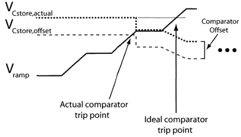
a conversion begins. The stepped-ramp generator produces the waveform Vstep shown in part (b) by ramping up one quantization level in voltage during every high portion of the global clock, and holding its output steady during every low portion of the global clock. The ramp generator operates in this manner until it has reached the highest possible voltage it can output, and then it resets for a new cycle. All of this occurs regardless of what happens in the local cells. During this ramping process, the memory cells' asynchronous comparators compare Vstep with their local version of VCstore, and output the result to their respective Digital Control block. Once a cell has determined that Vstep has exceeded VCstore, the switch S, closes during the next low cycle of the clock. Thus, the quantized value provided by Vstep is stored on Cstore. Finally, during the following high cycle of the clock, switch S2 enables the current source Ihalfbit, which subtracts % of a bit's worth of charge from Cstore. This final step allows leakage either onto or off of Cstore between restorations to be counteracted, as will be shown below. A magnified view of
S
1closes and
quantizes VCstore
Bi-directional leakage
can be tolerated
V
ramp
Ideal comparator
subtracts 1/2 bit
S2
closes and
trip point
Figure 2.2- Magnified view of Vramp and Vcstore signal behavior during the critical portion of the restoration cycle.
As was discussed above, limited amounts of leakage in either direction can be counteracted with this analog storage technique. However, this is true only if certain conditions are met. Figure 2.3 illustrates how much leakage can be tolerated between the N'h and the N+1th quantization cycle when the leakage is off of the capacitor. As long as
Quantization # N Quantization # N+1
Leakage off
of capacitorV
~st re
...
/
...
Cstre --.... :...V
----Vramp
bit
of leakage
Ideal comparator
can
be
tolerated
trip point
Figure 2.3 - A full /2 bit of charge leakage off of the capacitor can be counteracted with the quantized analog storage technique.
the leakage does not cause the stored voltage to move below the next lower quantized voltage value during the time of a full conversion cycle, the stored value can be re-quantized correctly. Thus, a full 2 bit of voltage leakage can be counteracted by the
memory element. Figure 2.4 illustrates the complementary situation where charge is leaking onto the storage capacitor between the Nth and N+lth quantization. Again, a full 2 bit of voltage leakage can be counteracted by the next quantization cycle. Thus, the condition that must be met in order to assure that leakage does not corrupt the stored
Quantization # N Quantization # N+1 Leakage onto capacitor
/...
...
...
...
V--
NUs
r...
N,
:..
-- . . .. . . .. - - --
-.
....
.
.. . .. . .
Vramp
1
bit of leakage
Ideal comparator
can be tolerated
trip point
Figure 2.4 - A full 2 bit of charge leakage onto the capacitor can be counteracted
with the quantized analog storage technique.
analog voltage is that the leakage must be less than 2 of a bit's worth of voltage over a full conversion cycle's worth of time, but the direction of the leakage does not matter. This condition assures that the stored analog voltage will never drift more than 2 bit from
its quantized level.
The above arguments proved that !2 of a bit of leakage can be counteracted with the quantized-analog technique on a value that was assumed to have been quantized the step before. However, there is also a boundary condition that must be analyzed in this
circuit. The cyclical storage pattern is broken when a new analog voltage is stored in the cell, as shown in Figure 2.5. In this figure, the value of VCstore is seen dropping from its previous value (somewhere above the current view) to its new value. In this worst-case example, the value of Vramp has just surpassed the new stored voltage value in the previous half-cycle. Thus, no quantization of the stored voltage will occur until a full conversion cycle later. Since the new voltage value is just larger than the 2 bit level of the ramp signal, it will drift (up in this case) by 2 of a bit to just above the next quantized
voltage level before the first time it is quantized. It is then erroneously quantized up, rather than down, leading to a full bit of quantization error. The value then remains in this bin from this point on, as would be expected from Figure 2.4. Thus, in the worst-case, the quantized-analog memory element may introduce a full bit of initial quantization error.
New Input Value Stored
Quantization # 1 Leakage onto capacitor ... ....
VCstore
...-
-..
[
Vramp
}
bit of leakage
Ideal comparator
Full bit of qpresent
trip point
ntization er
ua-ror
Figure 2.5 - This figure illustrates how a full bit of quantization error can occur
when a new value is stored in the memory cell.
This algorithm should be much more robust to process variation and circuit non-idealities than Hochet's implementation introduced in Section 1.2.5. The global ramp
generator ensures that a single analog voltage stored in any local cell will be quantized to the same voltage level (assuming the comparators have negligible input-offset voltages). The comparator's delay does not affect circuit operation as long as this delay, plus the time it takes to copy the ramp voltage to Cstore, is less than % of the clock period. Finally, because of the /2 bit subtraction, we no longer have to guarantee that the leakage is
unidirectional. In comparison with Cauwenbergh's implementation from Section 1.2.5, this cell is designed such that all of the information flow is from global circuits to local ones. Since the local circuits do not need to be able to drive a large analog bus with at least an N-bit precise voltage, where N is the accuracy of the storage cell, they do not need to consume as much power in this implementation. The global ramp generator is then the only circuit which must be capable of driving an N-bit accurate analog voltage across the chip, and so the power is spent in only one circuit block.
2.3 Chapter Summary
In this chapter, a list of design goals was developed for the analog memory cell. Some are merely qualitative, e.g. use as little area as possible, while others give more specific limits on power consumption, acquisition time, and hold time. The goals are listed in Table 2.1. After the design objectives were established, each of the analog memory techniques introduced in Chapter 1 was compared with the design goals, and a quantized-analog algorithm was chosen for the memory cell's implementation. Chapter 3 presents in detail the circuits used to implement this algorithm, SPICE simulations of these circuits, and SPICE simulations of the entire quantized-analog memory system.
3 Circuit Design & Simulations
The first two chapters have laid the foundation on which the remaining chapters are based. We examined existing approaches to analog storage and past implementations of analog storage circuits. Lessons learned from these implementations will aid in the design of the analog memory cell in this project. An algorithm and underlying circuit topology which should be able to meet the various design objectives that are required of the memory cell have also been developed. This chapter will first present the models used to describe MOS transistors in above-threshold operation. Next, it will introduce the basic circuit building blocks used in the memory cell, highlighting the most important features of each, and will compare hand-calculated parameters for the cells with SPICE simulations. After the constituent circuits have been examined, they will be used as "black boxes" to construct the overall topology, and SPICE simulations will be used to verify the overall system operation.
3.1 Large-Signal and Small-Signal Device Models
Before presenting the circuits used in this design, the large-signal and small-signal above-threshold MOS models are reviewed. The parameters used in the rest of this chapter and the next are all defined in this section.
3.1.1 Large-Signal Above-Threshold MOS Model
Figure 3.1 shows an NMOS transistor and defines its commonly-used forms of voltage and current variables. Figure 3.2 shows a family of operating curves depicting ID as a function of VDS for different values of VGS, with VSB= OV. These transfer curves
were simulated in SPICE using parameters extracted from the MOSIS 1.5p1m AMI CMOS process that will be used to fabricate the final memory cell. The figure shows two regions of transistor operation based on the external voltages: the triode region and the saturation region. These regions are separated by a dotted line plotting the points where
VDS = VGS-Vt. This particular value of drain-to-source voltage is known as VDsat because it is the voltage at which a transistor operating at a constant VGS moves from the
saturation to the triode region. The equation defining transistor operation in the triode region is
ID =hn Q~jJ(V GS t) VDS - VDS2 (2.2)
L 21c
where pn, is the mobility for electrons, Cox is the gate capacitance per unit area, W is the transistor gate width, L is the transistor gate length, K is a parameter representing the ratio
of control over the channel potential of the gate versus the bulk, Vt is the transistor's threshold voltage, and the remaining voltages are as they were defined in Figure 3.1. In the triode region, the transistor behaves like a resistor as long as the VDS2/2K term is
much smaller the (VGS - Vt)VDS term. This is true in the area near the origin, where the ID versus VDS curves look locally like straight lines - the same characteristic as a resistor. When this condition holds, the effective resistance of the MOSFET is given by the
D
Drain
C+
Gate
(
Bulk
V
VDS
VGS
+
SB
Source
Figure 3.1 - NMOS transistor symbol labeled with the voltage and current variables
typically used in describing its operation.
VG$= 3.OV
200
Triode
Region"
Saturation
Region
.
VGS=2.4V 150 - ... V ,- V 100- DS G VG 1.8V 50- -VGS'= 1.2V VGS= 0.6V 0.0 0.5 1.0 1.5 2.0 2.5 3.0 VDS
(V)
Figure 3.2 - ID versus VDS for different values of VGS. This data was simulated in
SPICE based on models from the MOSIS 1.5pm CMOS process that will be used for
equation
V 1
R eff D( (2.3)
D Pn( ~j(Gs ~ )
L
This region of operation is typically encountered in situations where the MOSFET is used as a switch.
The second region of operation for a MOSFET is the saturation region. Notice that in this portion of the curves, the value of VDS has only a small effect on the current flowing through the transistor -- effectively, the transistor looks like a current source with fairly high output impedance. This is the region of the MOS transistor that is used for amplification. The equation defining operation in the saturated region is
-,uC 0j1C VW _V
ID ~ )(GSt L DDsat) (2.4)
where all of the variables are the same as before, and k is a variable describing the change in drain current as a function of a change in the drain-to-source voltage. The parameter k is inversely proportional to transistor length, and is bias-point dependent.
An effect that was not taken into account in the previous two equations is the body effect. When the bulk is biased at a different voltage than the source, it causes the transistor exhibit the same characteristics as above, except with a different threshold voltage. The new threshold voltage is defined as
V, + y V=B + 20F F|) (2.5) where Vt is the overall threshold voltage, Vto is the threshold voltage when VSB= OV, y is the body-effect constant, and 2 F is the surface inversion potential.
As for PMOS transistors, all of the above equations are valid if a negative sign is placed in front of every voltage variable, pt is replaced by pp, and ID is defined as the source-to-drain current of the transistor.
3.1.2 Small-Signal Above-Threshold NMOS Model
As was mentioned in the previous section, a triode transistor looks very similar to a resistor for drain-to-source voltages close to zero. Therefore, its small-signal model is just a resistor from drain-to-source, with the resistance given by Equation 3.2. In addition to the channel resistance, there is capacitance from the gate to both the source and drain, through the conduction channel. The values of these capacitors are usually estimated as
Cg =sC, = WLC . (2.6)
There are also source-to-bulk and drain-to-bulk capacitances which will be very similar to the values in the saturated region of operation, so we will defer their defining equations until then. A simple triode region small-signal model with the parameters described above is shown in Figure 3.3.
Vg
cgs
rdS
Cgd
Vs
0
Vd
Csb
Cdb
Figure 3.3 - Small signal model of a MOSFET transistor operating in the triode region.