HAL Id: hal-02920181
https://hal.archives-ouvertes.fr/hal-02920181
Submitted on 7 Nov 2020
HAL is a multi-disciplinary open access
archive for the deposit and dissemination of
sci-entific research documents, whether they are
pub-lished or not. The documents may come from
teaching and research institutions in France or
abroad, or from public or private research centers.
L’archive ouverte pluridisciplinaire HAL, est
destinée au dépôt et à la diffusion de documents
scientifiques de niveau recherche, publiés ou non,
émanant des établissements d’enseignement et de
recherche français ou étrangers, des laboratoires
publics ou privés.
Modeling and Design of High Bandwidth Feedback Loop
for dv/dt Control in CMOS AGD for GaN
Plinio Bau, Marc Cousineau, Bernardo Cougo, Frédéric Richardeau, Nicolas
Rouger
To cite this version:
Plinio Bau, Marc Cousineau, Bernardo Cougo, Frédéric Richardeau, Nicolas Rouger. Modeling and
Design of High Bandwidth Feedback Loop for dv/dt Control in CMOS AGD for GaN. 2020 32nd
International Symposium on Power Semiconductor Devices and ICs (ISPSD), Sep 2020, Vienna (
virtual ), Austria. pp.106-109, �10.1109/ISPSD46842.2020.9170106�. �hal-02920181�
the main equations providing the link between feedback loop bandwidth and specific technology parameters are obtained. This optimization study allows us to determine the theoretical limits in terms of bandwidth and silicon area. Then, it becomes possible to determine the most appropriate switching control method to implement depending on the application requirements (high efficiency, low EMI), i.e. active feedback with adjustable gain, while ensuring suitable time delays. A feedback loop bandwidth of 1.59 GHz using an 1pF integrated capacitor to address a switching speed of 175 V/ns is demonstrated. Experimental results and simulations using accurate technology models confirms the theory.
Keywords—Active gate driver, GaN, switching analysis, dv/dt, EMI, power electronics, ASIC for power IC.
I. INTRODUCTION
Switching times of wide bandgap power transistors are extremely high (hundreds of V/ns for 600V GaN or 1.2kV SiC MOSFET) [1]. Therefore, practical useful guidelines are provided to the designer to determine the best trade-off in terms of integrated high voltage capacitive dv/dt sensor (CS), current mirror gain and PMOS/NMOS transistors sizes in order to design an
integrated dv/dt control system [2]-[4]. Systematic comparison between theoretical predictions and CADENCETM
simulation/layout use-case designs are investigated to demonstrate the validity of the approach. Experimental results confirm the theoretical study allowing the design of sub nanosecond response systems. At last, it becomes possible to determine the most appropriate technology to implement the AGD controlling high dv/dt of wide-bandgap transistors.
II. DV/DT CONTROL FEEDBACK LOOP
Fig. 1 shows the transistor level schematics of the proposed CMOS AGD. As already demonstrated in [2] from the same authors, the dv/dt can be controlled by changing the value of the gain. The gain is made by the width ratios of transistors involved in a PMOS and a NMOS current mirrors. By increasing this gain, the dv/dt of a power device can be reduced independently from the di/dt.
The main idea of this method is to sink a current from the gate node during the turn-on event. Therefore, a virtual capacitor is emulated, only during the dv/dt phase, between the gate and drain nodes of the WBG power device. One should note that this gain G results from the association of a first and second current mirror stages, respectively made of PMOS and NMOS transistors, obtaining G = GP × GN. Neglecting the load current effect and some other second order physical phenomena, the dv/dt can be
expressed by (1): ) GC (C R v v C i C R v v dt dv S rss G M DRV rss FB rss G M DRV DS (1)
Author version of the accepted article published in the IEEE ISPSD2020 proceedings –
https://doi.org/10.1109/ISPSD46842.2020.9170106
Fig. 1. Schematic of the AGD to control turn-on dv/dt values.
This work shows a step-by-step analytical analysis aimed to optimize the parameters of the circuit shown in Fig. 1, circuit previously presented in details in [2].
TABLEI
THEORETICAL EXPECTED DV/DT ATTENUATION
Attenuation factor (Att) dv/dt attenuation GCS/ Crss GCS (Crss=2pF) G (CS=1pF) 1 0% 0 0 0 4/3 25% 1/3 0.6pF 0.3 2 50% 1 2pF 2 4 75% 3 6pF 3 rss S CL DS OL DS tt C GC 1 dt dv / dt dv A (2)
where dvDS/dt|OL and dvDS/dt|CL and are respectively the open-loop and closed-loop vDS variations and Crss represents the
gate-to-drain capacitor during the Miller plateau.
Table I shows the value of the product GCs to consider for a given expected dv/dt attenuation Att for the GaN power device
GS66508T (Crss=2pF). Choosing an attenuation Att (for example 50% from 175V/ns to 87.5V/ns) the best distribution between
the values of G and CS has to be determined, both in terms of feedback loop bandwidth and silicon area. Next chapters present
optimization studies for a given constant GCS, related to a specific application (GCS=10pF, dvDS/dt|CL =80V/ns).
A. Feedback loop circuit model
Fig. 2(a) shows the feedback loop circuit used to control dvDS/dt considering the intrinsic capacitances CGSp and CGSn of the
PMOS and NMOS transistors. Fig. 2(b) provides a representation of the circuit layout showing the silicon area required for the transistors M1 to M4. The case with GP=2 and GN=2 for the gains of the two current mirrors M1-M2 and M3-M4 is illustrated.
An elementary size for the transistor M1 has to be chosen. This size depends both on the input current iCs provides by the
sensing capacitor CS and the minimum value of vinM that can be tolerated. It can be noticed that M2, M3 and M4 sizes depends
Fig. 2. (a) Two-stage current mirror with its parasitic capacitances, (b) Circuit layout assuming a area factor of 2.5 between NMOS and PMOS transistors (GP=2 and GN=2).
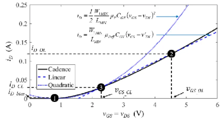
B. Sizing M1
Fig. 3 shows the characteristics of a diode-connected PMOS transistor. Due to short channel effect observed in submicron CMOS technologies, two different operating zones may be distinguished, a low current and a high current zones. Therefore, the classic square law has to be linearized for using the transistor at high current level, the well-known square law is no longer valid and a direct proportionality between drain current and gate-to-source voltage has to be considered. With parametric simulations, at vGS constant, it is observed a constant current per width ratio in a wide range of values for W1. Considering the length L of the
transistor channel minimum, this constant iD/W ratio is very useful to make the link between the size of the capacitor Cs in one
hand, and in the other hand the resulting size of the mirrors.
The transistor M1 will operate at the operating points 1, 2 and 3 indicated in Fig. 3. At the beginning, when no switching event occurs, iD=0. At first, slightly before a turn-on order, a pre-biasing current ibias (see Fig. 1) of about 50 µA is generated
biasing M1 at the point 1. Then, when a switching event occurs, the transistor M1 reaches the point 2 during a short transient less than 1ns. Just after a short delay, the feedback loop acts to reduce dvDS/dt, the current iCs decreases and M1 reaches the point
3. Then, it remains on this biasing point 3 for the rest of the switching, assuming a perfect trapezoidal vDS waveform. If vDS is not
perfectly trapezoidal, W1 will still operate between points 1 and 3.
Fig. 3 also shows that the temporary operating point 2 should not exceed the maximum voltage vDVR+0,6V otherwise the
protection diode DP may conduct and clamp the voltage to -0,6V. The minimum width of M1 is calculated to place point 3 at
vGS_CL=vDRV/2 and it is verified that point 2 will operate under safe operation area. Finally, the expression W1, the width of M1
is:
)
v'
(v
g
L
i
W
TH GS_CL mP MIN D_CL MIN 1
(3)where LMIN is the minimum transistor length possible of the technology to withstand 5V, 500 nm in our case, and v’TH is the
effective threshold voltage of the linear model shown in Fig. 3 around 1.5V. µPeff is the effective mobility of the PMOS transistor
Author version of the accepted article published in the IEEE ISPSD2020 proceedings –
https://doi.org/10.1109/ISPSD46842.2020.9170106
Fig. 3. Diode-connected transistor PMOS characteristic and 1st order model parameter extraction.
C. Sizing W3 as a function of W2
The transistor M2 is a multiple of M1 depending the gain GP of the 1st-stage current mirror. Now, sizing M3 to operate at
vDS3=VDRV/2 will make M2 always operate in its saturation region. Then, to guarantee the appropriate biasing of M3, the ratio
between W2 and W3 has to be equal to the ratio δ of the effective mobility of the PMOS and NMOS transistors. In our case, a ratio equal to 2.5 is obtained.
δ
W
W
2 3 with effP effNμ
μ
δ
(4)III. BANDWIDTH ANALYSIS
One expression for bandwidth as a function of gain or CS in order to address very fast transient response, with a constant
factor GCS imposed by the application, the bandwidth of the feedback loop has to be determined. Its value may depend on the
gains GP and GN and on the value of the capacitor CS. The total intrinsic capacitances at the gate of the PMOS and NMOS
current mirrors are respectively given by (5) and (6).
P
GSp S_PAR P S_PAR DSp v_p GDp P GSp P P C C G 1 C C C a 1 C G C G 1 C (5)
N
P GSn P DSp N DSp P DSn P v_n GDn P N GSn P N N C G C G G 1 C C G C G a 1 C G G C G G 1 C (6)where av_p and av_n are the small signal voltage gains of the common-source stage made by M2 and M4 respectively, both close
to one, and CGS, CGD and CDS, are the intrinsic capacitors of the transistors.
The expressions of the total capacitances CP and CN shown by the gate nodes of the PMOS and NMOS transistors can be
drastically simplified.
To calculate the bandwidth, knowing the capacitances of the circuit, the associated dynamic impedances have to be computed. Mainly, the impedances seen at the gate nodes are provided by the diode-connected transistors M1 and M3. Their values are related to the transconductances gm. The time constants
𝜏
can be written as follow:m3 DS2 N N m1 P P g g C ;τ g C τ (7)
where gm1 and gm3 are M1 and M3 transconductances and gDS2 is the drain-to-source admittance of M2.
can be related to this transition frequency. Because M1 and M3 are diode-connected transistors, they always work in their saturation region where CGD can be neglected comparing to CGS. Now, neglecting the contributions of CS_PAR and CDSp in Eq.
(5) and (6), one can estimate:
cN_est N T cN f G 1 f f (10) cP_est P T cP f G 1 f δ 1 f (11)
Fig. 5 shows a good correlation between simulated points in CADENCETM and the estimation expressed by Eq. (10).
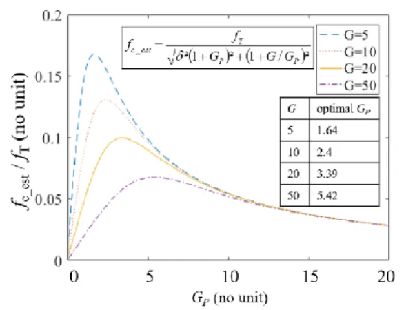
A. Gain G distribution between GP and GN
Depending on the distribution of the gain G among the two current mirror gains GP and GN, the overall feedback-loop
bandwidth fc changes. An optimal distribution can be identified. So, an expression of the bandwidth using a geometrical
averaging of the two time constants is proposed:
² 1/f ² 1/f
1/fc_est cN_est cP_est (12)
Fig. 4 shows the optimal choice of GP depending on the value of G. Note the higher G, the lower the bandwidth.
Fig. 4. Normalized cutoff frequency of the feedback-loop as a function of the PMOS mirror gain GP for several values of G.
B. Distribution between G and CS
For a targeted attenuation of dvDS/dt, the product GCS is imposed. Now, an optimal distribution of values between the gain
G and the capacitor CS, has to be determined to maximize the feedback loop bandwidth fc. Indeed, the higher CS, the lower G
Author version of the accepted article published in the IEEE ISPSD2020 proceedings –
https://doi.org/10.1109/ISPSD46842.2020.9170106
Fig. 5. Bandwidth of one NMOS current mirror as a function of its gain.
To compute accurately fc, all the intrinsic capacitances present in Eq. (5) and (6) are taken into account. Fig. 6 shows the
MatlabTM computations using the appropriate technology parameters with GC
S equals to 10pF. Simulation results using CS=
100fF, 1pF and 10pF confirm the theoretical projections.
Fig. 6. Feedback-loop bandwidth as a function of CS for a constant GCS = 10pF.
IV. SURFACE ANALYSIS
Now, considering a given product GCS constant, the separate values of G and CS have an impact on the silicon area required.
The surface SMp and SMp of the PMOS and NMOS current mirrors can be expressed respectively by:
P
MIN 1MIN Mp1
G
αL
W
S
(13)
P
MIN 1MIN MIN 3 MIN N P Mn W L δ α G G W αL G 1 G S (14)where α is the swell factor, i.e. the ratio between the active areas and the actual total area required by the transistors.
It should be noted that W1MIN is a function of the size of CS due to the increase of the current iD(CL) when CS increase. According
to Eq. (3) it is possible to write:
S CL DS MIN P S MIN 1 S CL DS TH GS_CL OX Peff MIN S MIN 1 C dt dv L J 1 ) (C W ; C dt dv V' V C L ) (C W 2 (15)where JP is the current density of M1 linked to the choice of vGS_CL (see Fig. 3).
The total silicon area Stot required for the proposed circuit is the surface of both current mirrors plus the in-chip high-voltage
Eq. (17) has a minimum value is achieved for low values of CS. Fig. 7 shows the surface Stot versus CS for a constant GCS
product. Stot increase proportionally with CS at high CS values.
Fig. 7. Silicon surface as a function of the input sensing capacitor CS for a constant attenuation product GCS=10pF.
V. EXPERIMENTAL RESULTS
In order to achieve the best bandwidth a higher value of CS is chosen even if it will consume more surface. It can be seen in
Fig. 5 the bandwidth is inversely proportional to the gain.
Fig. 8. (a) Experimental waveforms of AGD controlling dv/dt from 175V/ns to 120V/ns with in-chip HV capacitor of 1pF (b) microscope picture of the ASIC AGD
Fig. 8 (b) is the AGD designed with the high voltage in-chip capacitors. Attenuation factor of 1.45 (Att=175/120 V/ns) is
demonstrated in Fig. 8 (a) with CS=1pF and G=10. A difference between expected attenuation in dv/dt and obtained experiment
value is observed. The first reason is due to the presence of parasitic elements inside the chip and the PCB that are not taken into account in the theoretical study. The second reason is because some extra current is required to put M5 transistor in saturation mode before the feedback loop becomes effective.
Author version of the accepted article published in the IEEE ISPSD2020 proceedings –
https://doi.org/10.1109/ISPSD46842.2020.9170106
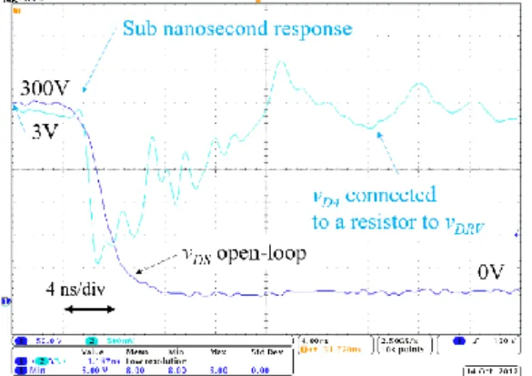
A sub-nanosecond response with the proposed technology is experimentally demonstrated. It can be seen in Fig. 8 the derivative of vDS of the GaN transistor starts to change in less than 1ns due to the feedback-loop effect. Fig. 9 shows the output
voltage of the feedback-loop starts to change in less than 1ns just after the GaN transistor vDS falling-edge.
Fig. 9. Experimental waveforms of the propsed system showing an open-loop response with a resistive load (RG=14.7Ω) connected to vDRV.
VI. CONCLUSION
This paper develops a theoretical analysis to provide the optimum distribution between the gains of the two current mirrors and the value of the sensing capacitor to maximize the bandwidth of a dv/dt feedback control loop. It is demonstrated that the bandwidth of the proposed circuit is correlated to the transition frequency of the CMOS technology. Therefore, choosing a technology with the highest transition frequency, with appropriate voltage capabilities to sustain 5V for GaN and 25V for SiC and IGBT applications, is the best choice. It is also demonstrated that for a given constant GCS product, the higher the sensing
capacitor CS, the higher the bandwidth for the feedback-loop. However, the silicon surface increase with CS and a trade-off has
to be considered.
REFERENCES
[1] D. Liu, H. C. P. Dymond, J. Wang, B. H. Stark and S. J. Hollis, "Building blocks for future dual-channel GaN gate drivers: Arbitrary waveform driver, bootstrap voltage supply, and level shifter," (ISPSD), Shanghai, China, 2019.
[2] P. Bau et al., "Sub-Nanosecond Delay CMOS Active Gate Driver for Closed-Loop dv/dt Control of GaN Transistors," 2019 31st (ISPSD), Shanghai, China, 2019, pp. 75-78.
[3] R. Wang et al., "Self-adaptive active gate driver for IGBT switching performance optimization based on status monitoring," in IEEE Transactions on
Power Electronics. 2020
[4] L. Y. Ling, Z. Zhao and Y. Zhu, "A Novel Digital Active Gate Driver For High-Power IGBT To Reduce Switching Losses And Stresses," 2019 IEEE Energy Conversion Congress and Exposition (ECCE), Baltimore, MD, USA, 2019.
[5] H. Li, Y. Jiang, C. Feng and Z. Yang, "A Voltage-injected Active Gate Driver for Improving the Dynamic Performance of SiC MOSFET," 2019 IEEE Energy Conversion Congress and Exposition (ECCE), Baltimore, MD, USA, 2019
[6] L. Shu, J. Zhang and S. Shao, "Crosstalk Analysis and Suppression for a Closed-Loop Active IGBT Gate Driver," in IEEE Journal of Emerging and Selected Topics in Power Electronics, vol. 7, no. 3, pp. 1931-1940, Sept. 2019