HAL Id: hal-01067989
https://hal.archives-ouvertes.fr/hal-01067989
Submitted on 24 Sep 2014
HAL is a multi-disciplinary open access
archive for the deposit and dissemination of
sci-entific research documents, whether they are
pub-lished or not. The documents may come from
teaching and research institutions in France or
abroad, or from public or private research centers.
L’archive ouverte pluridisciplinaire HAL, est
destinée au dépôt et à la diffusion de documents
scientifiques de niveau recherche, publiés ou non,
émanant des établissements d’enseignement et de
recherche français ou étrangers, des laboratoires
publics ou privés.
Measurements within Complex Digital SoC
Lionel Vincent, Edith Beigné, Laurent Alacoque, Suzanne Lesecq, Catherine
Bour, Philippe Maurine
To cite this version:
Lionel Vincent, Edith Beigné, Laurent Alacoque, Suzanne Lesecq, Catherine Bour, et al.. A Fully
Integrated 32 nm MultiProbe for Dynamic PVT Measurements within Complex Digital SoC. VARI:
International Workshop on CMOS Variability, May 2011, Grenoble, France. �hal-01067989�
Abstract—This paper deals with the design of a compact Process, Voltage and Temperature (PVT) probe architecture, in 32nm CMOS technology. The sensor, hereafter named MultiProbe, is composed of 7 different ring oscillators, each one presenting a particular sensitivity to PVT variations. The architecture allows MultiProbes to be chained, so that a single controller is needed. Simulation results exhibit the non-linearity behavior of the ring oscillators under temperature and voltage variations as well as their particular behavior. Due to their small size, the Multiprobe blocks can be easily integrated within a complex digital SoC architecture.
I. INTRODUCTION
ING-oscillators are widely used as sensors to monitor effects of Temperature (T), Voltage (V), and Process (P) variations on the timings of CMOS logic gates [1-3], and on critical paths. Former works have made use of such sensors frequency shifts under PVT variations to ensure a safe functional mode [4], or to estimate the operating frequency as a function of V and T [1]. First probes dedicated to process variation monitoring were implemented as static sensors to quantify, after fabrication, the process variations along the chip, from die-to-die, or from wafer-to-wafer [3], and then to estimate the maximum attainable performance of a chip after post silicon characterization.
Several works have proposed smart sensors to differentiate Temperature from Voltage effects and to provide dedicated sensors. Zero Temperature Coefficient (ZTC) property has been used in [5] to design a Voltage sensor. [6] proposes IR-drops measurements via the difference between two identical Ring-Oscillators (RO) with separate power supplies. ROs with temperature controlled frequency were reported in [7] and [8]. Both works rely on a chain of current-starved inverters whose propagation delay is controlled by a biasing voltage. In both approaches, temperature is deducted from the frequency difference of two ROs with different temperature dependencies. The three variables (P, V, and T) exhibit very different dynamic evolutions. [9] presents the wide range of Voltage drops dynamics (1kHz to 100GHz) while Temperature variations can be estimated around 1MHz and Process is usually considered constant during the life-time, except in case of wearout. The difficulty of designing this kind of sensors remains in the fact that the whole dynamics has to be sensed.
1Lionel Vincent, Edith Beigné, Laurent Alacoque, Suzanne Lesecq and Catherine Bour are with CEA-LETI MINATEC Campus, 17 rue des martyrs, 38054 Grenoble Cedex 9, France, {firstname.name}@cea.fr
²Philippe Maurine is with the Laboratoire d'Informatique, de Robotique et de Microélectronique de Montpellier (LIRMM), Université Montpellier 2, UMR 5506 – CC477, 161 rue Ada 34095 Montpellier, Cedex 5, France (e-mail: [email protected]).
This paper aims at presenting a compact PVT sensor IP easy to be integrated into a complex digital SoC architecture. This IP, denoted by MultiProbe afterward, is based on several ROs multiplexed all together so as to meet the main constraints applying to all on-chip sensors: (1) a very low area, (2) a wide dynamic of frequency measurements, (3) an easy integration and (4) a capability to discriminate P, V and T impacts with a minimum set of measurements. Distributed over the SoC, MultiProbes IPs may provide dynamic PVT variation measurements to both global and local system controllers. Coupled with the observation of critical paths and with specific algorithms allowing P, V and T discrimination, these measurements are used in adaptive Voltage and Frequency scaling architectures to reach the optimum energetic point, in presence of PVT variations while meeting the required applicative performances.
In this paper, the design of the MultiProbe IP, as a set of 7 PVT probes based on 7 different ROs, is presented. All the constituting RO are sensitive to variations but in a slightly different way. For modularity purpose, all the distributed MultiProbes are chained so that a unique controller has to be implemented. Section II gives the MultiProbe architecture. The full architecture is first described, and then the ring oscillators are presented with an emphasis on the Dedicated Temperature sensor. Section III summarizes the MultiProbe control and section IV reports the behavior of 2 particular probes, results being obtained from post layout simulations.
II.MULTIPROBE ARCHITECTURE PROPOSAL
The MultiProbe is a low area on-chip macro-block embedding several Ring Oscillators (ROs) as PVT sensors. The MultiProbe Controller is integrated only once for an IP to be sensed whereas the MultiProbes are distributed close to the monitored circuit point. Using a daisy chain, several MultiProbes can be implemented for a single controller with common input/output signals.
A. Full architecture
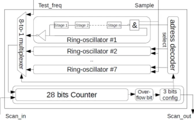
The architecture proposed for the MultiProbe, (see Figure 1), includes 7 different ROs as sensors, an address decoder to select the running RO, an 8-to-1 multiplexer to output the selected RO frequency, and finally 32 bits register. This register is partitioned into 28 bits for counting, an overflow bit and the 3 bits to configure the RO selection. All parts of the MultiProbe are made of standard cells from 32nm technology libraries.
The register has a dual functionality depending on the selected mode: sampling or scanning. During the sampling
A Fully Integrated 32 nm MultiProbe for Dynamic PVT
Measurements within Complex Digital SoC
L. Vincent
1, E. Beigné
1, L. Alacoque
1, S. Lesecq
1, C. Bour
1, Ph. Maurine
2mode the counter computes the number of rising transition occurring at the output of the selected RO, while the “sample” pin is activated. The scanning mode, allows in one hand lifting the data contained in the register throughout “scan_out” and in the other introducing the 32 new bits, containing the new configuration, via the “scan_in” input. As a result of this communication protocol, each measure is necessarily followed by a scanning.
The address decoder activates a single sensor according to the chosen configuration stored in the register. Thus, a single RO operates at a time. This operating mode avoids RO frequencies coupling, occurring when all RO run simultaneously and could bias the PVT variation monitoring.
Figure 1: Scheme of the MultiProbe architecture proposed The principle of sensors based on RO is to measure their output frequency by counting the number of rising edges occurring during a sensing time window of chosen duration. Because their output frequency depends on the Process quality and the averaged value of V and T over the sensing time window, ROs may be used as PVT sensors.
B. Ring oscillators
A Ring Oscillator (RO) is an unstable closed-loop system. As shown in Figure 1, each RO is made of a chain of several stages and a 3-input NAND gate. This latter activates the sensor with the two inputs “sample” and “select”. All stages of one RO are identical but they are different from one RO to another. Each delay cell acts as a buffer, thus the RO oscillates due to the inverter NAND function.
1) Probe dedicated to temperature sensing
In this work, a temperature dependent RO based on current-starved inverters biased by a thermally dependent current generator is proposed.
a)Current-starved inverters
Current-starved inverters are inverters with additional current limiting transistors that can also be used as clock-gating circuits when the RO is disabled. Figure 2 (left) shows the current-starved delay cell used in the proposed architecture. To save silicon area, the relatively large polarization transistors M1 and M6 are shared by a pair of inverters.
Because of the current limitation, during a transition, each inverter loads its output capacitance at constant current. This results in a slower, linear, output voltage swing.
As it has been shown in [7], when the current is sufficiently low, the current limiting dominates the gate delay and the propagation time td can be expressed as:
bias L H load d C V V I t ≈2 ( − )/ (1)
where Cload is the output capacitance of each stage, VH-VL is
the output voltage swing and Ibias is the biasing current
imposed by transistors M1 and M6. When N delay cells are used in the loop, the RO frequency can be expressed as [7]:
)] ( . . 4 [ / ) . . 2 /( 1 Ntd Ibias NCload VH VL f = ≈ − (2)
As can be seen from (2), the RO frequency is proportional to the biasing current. The biasing cell is responsible for the generation of a temperature dependent current on the basis of MOSFET thermally dependent parameters.
Figure 2: Delay cell (left), temperature dependent biasing (right) b)Thermally dependent biasing cell
In MOSFET, the mobility of carriers and the threshold voltage parameters dominate the temperature dependence. They can be modeled as:
) ( ) ( ) ( ) / )( ( ) (T =µT0 T T0 −k VT T =VT T0 −α T−T0 µ (3)
with T, T0 the circuit and reference temperatures, µ the
mobility, VT the threshold voltage and k and α two positive
technology-dependent parameters.
Note that a unique biasing cell is used to bias all delay-cells in the RO, as can be seen on Figure 2 (right). It is made of two diode-connected complementary MOSFETs. This structure ensures the saturation of both transistors as long as VDD > (VTP+VTN). This current-matching structure constrains
its both transistors operating with a lowest Vgs-Vth than others digital transistors (composing the others ROs). This magnifies Vth relative variations regarding others ROs and hence the impact of relative variations on the biasing current is increased. The cell was tuned to maximize temperature sensitivity and linearity of its output value around the nominal supply voltage value (VDD=1.0V).
c)Results
The resulting Ring Oscillator (RO) frequency of Figure 3 was extracted from electrical transient simulations at different temperatures for both the thermally-dependent and the standard Ring Oscillators. As shown, the RO exhibits a sensitivity of 14.1 MHz/K whereas standard inverters show a lower sensitivity, (0.7 MHz/K). This high sensitivity to temperature ensures a finer discrimination and discretization of temperature evolution.
Figure 3 : RO frequency vs temperature (at Vdd = 1V); (blue diamond) thermally dependent (red square) standard-inverters RO.
2) Description of the 6 other probes
The 6 other ROs constituting the MultiProbe architecture are designed with standard cells. Each RO is made of a different number of stages, and the stage of each sensor is different in terms of gate type and/or layout (see Table 1 for a summary). They have been chosen because of their large sensitivity to PVT variations in any technology and because they do behave as any critical path of a circuit. The output frequency of each sensor is around 1GHz fitting the internal 32-bits counter frequency.
TABLE 1: RING OSCILLATORS DESCRIPTION
RO Name Description of Stage Gate type Inverters 13 stages of 2 standard inverter cells
Long wires
10 stages of 2 inverters linked together with long wires using several metal layers and vias. Latch 5 stages made of 1 latch standard cells
Xor 8 stages made of 1 XOR standard cells. Ncap 6 stages of 2 inverters loaded with capacitors
made of a NMOS transistor.
Pcap 6 stages of 2 inverters loaded with capacitors made of a PMOS transistor.
Figure 4 gives the layout of the long wire delay cell (right) to be compared with the similar short wire delay cell (left).
Figure 4: delay cell layout of inverter (left) and long-wire inverter (right)
III. MULTIPROBE DIGITAL CONTROL
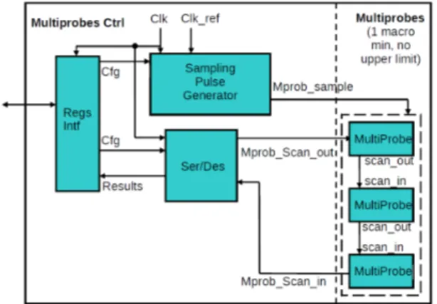
An important advantage of chained MultiProbes architecture is that a single fully digital controller is needed to monitor several probes, limiting the silicon area and wires. The goal of the controller (Figure 5) is to handle
MultiProbes, by sending and retrieving data to and from them, but it also controls the sampling procedure.
The Register interface “Regs Intf” communicates with the global on-chip communication network. The Seria-lizer/Deserializer “Ser/Des” block respectively sends and receives data to and from the chained MultiProbes. It communicates with the Register interface to store results and to receive the next configuration (Cfg). The programmable sampling pulse generator aims to accurately control the pulse width during which the sensors are activated.
Figure 5: Global scheme of the MultiProbe control
IV. PVTCORNER SIMULATION RESULTS
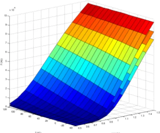
The behavior of Ring Oscillators under Temperature and supply Voltage variations, at a given Process corner is simulated at Spice level after RC extraction. Simulation results are obtained when the supply Voltage is swept from 0.5V to 1.5V by step of 0.1V and the Temperature varies from -40°C to 120°C by 10°C steps. The three cases of Process simulated are Slowest (SS), Typical (TT) and Fastest (FF) corners. The frequency F is measured under PVT variations, for two particular ROs: the Temperature Dedicated probe and the Inverter probe.
A. Dedicated Temperature probe simulation
This sensor has been specifically designed to be more sensitive to Temperature than the other ones. Figure 6 shows its characteristic surfaces. As shown, these surfaces are non linear. Each surface equation can be fitted, using a least squares method, into:
a fifth order in Voltage and, a second order in Temperature polynomial (or posinom).
By nature, the polarization cell has a high dependence on VDD variations. A linear increase of VDD results in a quadratic
augmentation of the biasing current, and thus of the RO frequency. Actually, near the nominal VDD (1V), the
frequency dependence in Temperature is nearly linear, as forecasted in II.B.1.b).When VDD is higher, the biasing
current gets large enough to stop limiting the inverter speed and the delay-cells behavior becomes similar to standard
2 3 32 4 41 5 50 2 2 22 3 31 4 40 2 12 2 21 3 30 2 02 11 2 20 01 10 00 T V P T V P V P T V P T V P V P T V P T V P V P T P T V P V P T P V P P Ftyp ⋅ ⋅ + ⋅ ⋅ + ⋅ + ⋅ ⋅ + ⋅ ⋅ + ⋅ + ⋅ ⋅ + ⋅ ⋅ + ⋅ + ⋅ + ⋅ ⋅ + ⋅ + ⋅ + ⋅ + = (4)
inverters. On the other-hand, when VDD < (VTP + VTN), both
polarization transistors are in sub-threshold region and the biasing current decreases and quickly approaches 0. As a result, the RO oscillates very slowly, as illustrated by the bended corner on the bottom right of Figure 6.
Figure 6 : Characteristic surfaces for the Temperature Dedicated probe F=f(V,T) for the 3 Process cases SS, TT, FF upward. B. Inverter probe simulation
This RO is the simplest one in the MultiProbe and it may be considered as the reference sensor.
Figure 7 : Characteristic surfaces for the Inverter ring-oscillator. F=f(V,T) for the 3 Process cases SS, TT, FF upward With the same simulation scenario, each characteristic surface of this RO is obtained on Figure 7. As can be seen, the behavior is highly non linear in V and T. Fitting the surface equation of the inverter probe response with a least squares method leads to:
which is a fourth order in Voltage and second in Temperature polynomial. Note that in [1], the non-linearity was identified to an order 4. However this result was obtained considering a micrometric technology (2µm) and above the Temperature Inversion Point. In [10], the probe behavior is totally different from the present probe behavior, with non-linearity in 1/V².
The ZTC effect around 1.2V can also be observed, and so the best case corner moves to [-40°C, 1.5V] operating point.
Note that the characteristic surfaces of the 5 other ROs are similar to that of the inverter probe. Therefore, they can be approximated by similar polynomials.
V.CONCLUSION AND FUTURE WORK
The architecture and design of a compact digital PVT sensor, named MultiProbe, and its controller have been presented. The proposed structure, distributed over a complex digital SoC, allows a dynamic PVT measurement within the circuit. The probes are based on ring-oscillators sensitive to PVT variations that were chosen to allow the discrimination of P, V and T dynamic evolution during sensing. A single controller is implemented to access several chained MultiProbes, limiting drastically the silicon area and routing overheads compared to former approaches. RC simulations have confirmed the non-linear behavior of ring-oscillators under Temperature and Voltage variations, in low voltage 32nm CMOS technology.
Implemented into an adaptive Voltage and Frequency scaling architecture, the fusion of information provided by all these probes will be performed in a future work to dynamically monitor the PVT variations. The main challenge is to adapt the control law of the DVFS policy to reach an optimum energetic functional point.
ACKNOWLEDGMENT
This work has been done in the context of the Platform 2012 program, a joint project between STMicroElectronics, CEA and the UE (ENIAC Joint Undertaking) in the MODERN project (ENIAC-120003). Authors also wish to associate Sylvain Miermont to this work.
REFERENCES
[1] G. Quénot, N. Paris, B. Zavidovique, “A temperature measurement cell for VLSI circuits”, Euro ASIC '91, pp. 334-338, 1991.
[2] M. Bhushan, A. Gattiker, M.B. Ketchen, and K.K. Das, “Ring Oscillators for CMOS Process Tuning and Variability Control”, IEEE Trans on Semiconductor Manufacturing, Vol. 19, pp. 10-18, 2006.
[3] M. Nekili, Y. Savaria, and G. Bois, “Spatial characterization of process variation via MOS transistor time constants in VLSI and WSI”, IEEE Journal of Solid-State Circuits, pp. 80-84, 1999.
[4] D. Wolpert, P. Ampadu, “A low-power safety mode for variation tolerant systems-on-chip”, IEEE International Symposium on Defect and Fault Tolerance of VLSI Systems, pp. 33-41, 2008.
[5] S.S. Prasad, P. Mandal, “A single circuit solution for voltage sensors”, IEEE International Symposium on Circuits and Systems, Vol. 4, pp. 3865-3868, 2005.
[6] Z. Abuhamdeh, V. D’Alassandro, R. Pico, D. Montrone, A. Crouch, A. Tracy, “Separating temperature effects from ring-oscillator reading to measure true IR-drop on chip”, IEEE International Test Conference, pp. 1-10, 2007.
[7] B. Datta, W. Burleson, “Low-power and robust on-ship thermal sensing using differential ring oscillators”, 50th Midwest Symposium on Circuits and Systems, pp. 29-32, 2007.
[8] Poki Chen, Chun-Chi Chen, Chin-Chung Tsai, Wen-Fu Lu, "A time-to-digital-converter-based CMOS smart temperature sensor", IEEE Journal of Solid-State Circuit, Vol.40, no.8, pp. 1642-1648, 2005.
[9] A.Muhtaroglu, G. Taylor, T. Rahal-Arabi, “On-die droop detector for analog sensing of power supply voltage”, IEEE Journal of Solid-State Circuits, pp. 651-660, 2004.
[10] J.J.L.Franco, E. Boemo, E. Castillo, L. Parrilla “Ring oscillators as thermal sensors in FPGAS: Experiments in low voltage”, Programmable Logic Conference (SPL), pp. 133-137, 2010. 2 2 22 3 31 4 40 2 12 2 21 3 30 2 02 11 2 20 01 10 00 T V P T V P V P T V P T V P V P T P T V P V P T P V P P Ftyp ⋅ ⋅ + ⋅ ⋅ + ⋅ + ⋅ ⋅ + ⋅ ⋅ + ⋅ + ⋅ + ⋅ ⋅ + ⋅ + ⋅ + ⋅ + = (5)