HAL Id: hal-01973334
https://hal.sorbonne-universite.fr/hal-01973334
Submitted on 16 Jan 2019
HAL is a multi-disciplinary open access
archive for the deposit and dissemination of
sci-entific research documents, whether they are
pub-lished or not. The documents may come from
teaching and research institutions in France or
abroad, or from public or private research centers.
L’archive ouverte pluridisciplinaire HAL, est
destinée au dépôt et à la diffusion de documents
scientifiques de niveau recherche, publiés ou non,
émanant des établissements d’enseignement et de
recherche français ou étrangers, des laboratoires
publics ou privés.
M. Kazar Mendes, E. Martinez, J.M. Ablett, M. Veillerot, R. Gassilloud, et al.. Chemistry of resistivity
changes in TiTe/Al2O3 conductive-bridge memories. Scientific Reports, Nature Publishing Group,
2018, 8 (1), pp.17919 (2018). �10.1038/s41598-018-36131-7�. �hal-01973334�
Chemistry of resistivity changes
in TiTe/Al
2
O
3
conductive-bridge
memories
M. Kazar Mendes
1, E. Martinez
1, J. M. Ablett
2, M. Veillerot
1, R. Gassilloud
1, M. Bernard
1,
O. Renault
1, J. P. Rueff
2,3& N. Barrett
4We report the chemical phenomena involved in the reverse forming (negative bias on top electrode) and reset of a TaN/TiTe/Al2O3/Ta memory stack. Hard X-ray photoelectron spectroscopy was used to conduct
a non-destructive investigation of the critical interfaces between the electrolyte (Al2O3) and the TiTe top
and Ta bottom electrodes. During reverse forming, Te accumulates at the TiTe/Al2O3 interface, the TiOx
layer between the electrolyte and the electrode is reduced and the TaOx at the interface with Al2O3 is
oxidized. These interfacial redox processes are related to an oxygen drift toward the bottom electrode under applied bias, which may favour Te transport into the electrolyte. Thus, the forming processes is related to both Te release and also to the probable migration of oxygen vacancies inside the alumina layer. The opposite phenomena are observed during the reset. TiOx is oxidized near Al2O3 and TaOx is
reduced at the Al2O3/Ta interface, following the O2− drift towards the top electrode under positive bias
while Te is driven back into the TiTe electrode.
Resistive Random Access Memories (RRAM) are candidates for the next generation of non-volatile memories (NVMs) thanks to their switching properties1,2. Among them, conductive bridge random access memories
(CBRAMs) are one promising solution to improve the cycling endurance while maintaining good scaling and high operation speed3–5. In these devices, an electrolyte (chalcogenide or a suitable oxide, for instance) is used as
a dielectric layer whose resistive state is changed by the diffusion of cations from the active electrode, containing most often Ag or Cu1,4,6 to form a conducting bridge. Changes in resistivity are explained by the formation and
partial destruction of Ag or Cu-rich filaments inside the electrolyte. The filament creation known as forming, is an irreversible process required to enable the write/erase (SET/RESET) cycles of the memory cell. The CBRAMs structures are characterized by higher resistance windows7, i.e. the ratio between the high (HRS) and low (LRS)
resistance state, compared to transition metal oxide-based RRAMs (OxRRAMs), and also by lower programming currents.
Recently, devices containing an elemental semiconductor such as tellurium, operating with reduced currents and less retention failures of the LRS8 have drawn special attention. In these subquantum CBRAM cells, the
fila-ment is thought to contain tellurium, yielding a 1-atom conductance (G1atom), significantly reduced compared to
standard CBRAMs and thus allowing low power operation. Subquantum CBRAMs based on an Al2O3 electrolyte
and an active top electrode of a Te binary alloy such as ZrTe, TiTe and HfTe, are the most promising systems with cell operating current and power as low as 10 µA and 0.01 mW8. The origin of resistive switching in Te-based
subquantum memories with ZrTe active electrode is attributed to the release of Te following Zr oxidation due to oxygen scavenging from the Al2O3 under the electric field9. Note that Te-filaments have also been observed in
CBRAMs based on Ge2Sb2Te5 (GST) sandwiched between inert electrodes (Ti and Pt). In the case of GST
contain-ing a Te-rich interfacial region, the resistive switchcontain-ing is no longer related to the usual phase change mechanism. The LRS was shown to be semiconducting and due to Te ions migration and reduction at the opposite electrode10.
TiTe features a retention behaviour controlled by a similar critical conductance as that for ZrTe8. The
investi-gation of this memory cell mechanism is important since not all binary alloys of Te favor the formation of a semi-conductor filament. For example, in the case of the CuTex the filament is formed preferentially by Cu11. Therefore,
1Univ. Grenoble Alpes, CEA, LETI, 38000, Grenoble, France. 2Synchrotron SOLEIL, l’Orme des Merisiers, Saint-Aubin,
F-91192, Gif-sur-Yvette Cedex, France. 3Sorbonne Université, UPMC Univ Paris 06, CNRS, UMR 7614, Laboratoire
de Chimie Physique-Matière et Rayonnement, 75005, Paris Cedex 05, France. 4SPEC, CEA, CNRS, Université
Paris-Saclay, CEA Paris-Saclay, 91191, Gif-sur-Yvette, France. Correspondence and requests for materials should be addressed to M.K.M. (email: munique.kazarmendes@cea.fr)
Received: 31 January 2018 Accepted: 14 November 2018 Published: xx xx xxxx
it is necessary to understand the role of the metal and the semiconductor during the resistance switching for each Te-based electrode variant.
Here, we investigate the negative forming, also called reverse forming, in which a negative voltage is applied to the top electrode and the first reset step i.e. from LRS to HRS. The reverse forming was analysed in this case since the positive polarisation caused an irreversible switching of the TiTe/Al2O3 cell unlike the negative polarization
that enabled the reset of the memory after the forming process. Negative forming was observed in several stand-ard Cu-based CBRAMs structures12–14 and reported to be related to metal cations and/or oxygen vacancies (V••
o).
Compared to positive forming, the bottom electrode, here Ta, may also play a role in addition to the top TiTe electrode.
In these complex systems, the interfaces between the electrodes and the solid electrolyte is known to play a critical role15. Composition changes at these interfaces are very often observed, even for RRAMs showing
filamentary-type switching. Regarding OXRRAMs, metals with high oxygen affinity (Ta, Ti…) are often used as electrodes. They form interfacial oxides that change the electrolyte composition by oxygen exchange. For exam-ple, in the ZrO2/Ti system, it has been shown that a TiOx film is created at the interface which in turn reduces the
oxide matrix to form ZrO2−x16. This is also the case for a metal in contact with its stoichiometric oxide, as reported
for the Ta/Ta2O5 system where an intermediate TaO2 oxide is formed17. For CBRAMs, the typical interface
inter-action involves the metal oxidation with the insertion of oxidized ions in the electrolyte. For example, in the Cu/ SiO2 system, Cu oxidation was found to provide Cu2+ ions diffusing from the top electrode inside the electrolyte
and participating in the resistive switching18. Similar effects were also reported near the bottom electrode19. All
these interfacial interactions may strongly influence the behavior of the memory cell and is also the case for Te-based subquantum CBRAMs in this paper.
More information about resistive swithing would facilitate the control and manufacturing of such memory cells. It is also necessary to better understand the cycling of the cell. Thus, not only the electroforming step9, but
also the switching between the LRS to the HRS, known as the RESET step must be investigated. To study the resis-tive state-dependent chemistry in such Te-based CBRAMs requires advanced characterization techniques. X-ray photoelectron spectroscopy is particularly interesting because it provides information about the chemical states. Hard X-ray photoelectron spectroscopy (HAXPES) enables non-destructive analysis of the buried interfaces between realistic electrodes and insulating layer thanks to the much greater probing depth20. Another advantage
of HAXPES compared to laboratory XPS is related to the high brightness offered by third generation synchrotron sources (1021–1022 photons/s/mm2/mrad2/0.1% BW). This can be used to highlight additional changes of the
whole matrix accompanying the filament formation, in particular interface modifications. The technique has already been successfully used to investigate the redox reactions that occurs during the resistive switching of oxide-based resistive memories21–23 and CBRAMs9.
We have used HAXPES to study the physical chemistry of forming and resistive switching of TiTe/Al2O3/Ta
CBRAMs. We compare results obtained for three samples: as-grown i.e. the pristine device with an HRS, formed i.e. the sample after the first transition between HRS and LRS and reset i.e. the sample after the first transition from LRS to HRS. The aim is to clarify the switching mechanisms and understand the chemical changes at both interfaces. As reported by Cho et al.24, the oxidation/reduction reactions at metal/oxide interfaces induce the
formation of intermediate layers that can influence the resistive switching. Note that the forming process implies a negative bias on the top electrode and so strictly speaking is reverse forming, however, hereafter we will refer to the process simply as forming.
Methods
The CBRAM is the TaN/TiTe/Al2O3/Ta structure (see Fig. 1(a)). The bottom electrode was a 200 nm-thick Ta
layer, deposited on a 200 mm Si (100) wafer. The 5 nm TiTe and Al2O3 layers were grown by physical vapor
dep-osition (PVD) at room temperature. The growth process was optimized to reach a Ti/Te stoichiometry of 40/60. The base pressure in the deposition chamber was 5 × 10⁻⁴ mbar. Finally, a 5-nm TaN capping layer was deposited
by reactive sputtering at 50 °C to prevent oxidation of TiTe when exposed to air. The TaN and TiTe layers were deposited through a mask to define a 2 mm diameter top electrode.
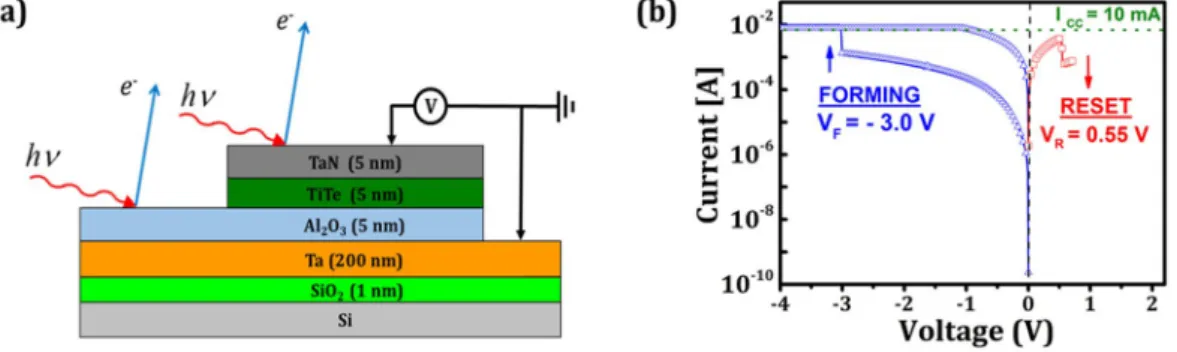
Figure 1. (a) Schematic of the TaN/TiTe/Al2O3/Ta device structure of the HAXPES measurements and
schematic of the setup for electrical characterization (b) I-V curve for the forming and the reset of the TaN/ TiTe/Al2O3/Ta stack.
The CBRAM structures were analysed in the as-grown state, after forming and after reset. The switching was performed in ambient atmosphere using a Keithley 2635B and the Ta bottom electrode was grounded. A linear voltage sweep was applied by an Au tip with minimum contact force on the TaN (Fig. 1(a)) at 0.1 V/s, between 0 and −4 V for the electroforming step and from 0 to 0.7 V for the reset step. A standard electrical connection was not used for the top electrode because the ultra-thin alumina layer can be easily short-circuited by mechanical or thermal stress. The electrical contact to the bottom electrode was made with a W tip. The compliance current of 10 mA (0.03 mA.cm−2) was chosen to avoid permanent breakdown of the oxide while inducing significant ionic
diffusion, facilitating the detection3.
HAXPES analyses were performed at the GALAXIES beamline of the SOLEIL synchrotron25. All
measure-ments were performed at room temperature. The TiTe electrode, the TiTe/Al2O3 interface, the thin oxide film
(Al2O3) and the bottom Al2O3/Ta interface were probed by tuning the inelastic mean free path (λ) using photon
energies of 6.9, 8 and 10 keV. The values of λ are estimated with the Tanuma equation26 for Al 1s, Ti 1s, Te 3d
3/2
and Ta 3d5/2 photoelectrons and are given in Table 1. These values are obtained by averaging the IMFPs27 for each
layer crossed by the photoelectrons during their transport toward the surface, weighted by the thickness of each layer (see Supplementary Information). The overall energy resolution (beamline and spectrometer) was 110, 160 and 210 meV for 6.9, 8 and 10 keV photon energies respectively.
The X-rays beam spot size on the sample was 500 × 30 µm2 (with an X-ray incidence angle of 10° with respect
to the surface) and photoelectrons emitted at an angle of 80° with respect to the surface were collected with a hemispherical SCIENTA EW4000 electron analyzer. The binding energy was calibrated relative to the Au 4f level measured from a clean gold surface and also relative to the Ta 3d5/2 level measured on the Al2O3/Ta interface
out-side the device areas (as a stable internal reference). The deconvolution of the core level spectra was performed using the Casa XPS software, version 2.3.16 from Casa Software Ltd. Backgrounds for XPS spectra were of the Shirley type28. The oxide peaks were modeled using a convolution of Lorentzian (30%) and Gaussian (70%)
func-tions while the metallic/semiconductor core lines were fitted using a Doniach-Sunjic function29. The peaks fit was
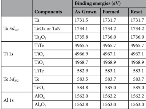
made establishing constrains on components positions and fixing the separation between each chemical state. All the details regarding the binding energies used for fitting are presented in Table 2.
Time-of-flight secondary ion mass spectrometry (ToF-SIMS) was used to study the elemental distribution depth profiles and possible interdiffusion for as-grown, formed and reset samples. ToF-SIMS data were collected using an ION-TOF ToF-SIMS 5 instrument. The Bi3+ analysis beam generated by a bismuth source, was
accel-erated at 25 keV and rastered over an area of 80 × 80 μm. Cesium ions were used for sputtering, rastered over a 300 × 300 µm² area, at an impact energy of 500 eV. Both beams were incident at 45°. The intensities of the M+ ions
and MCs+ clusters secondary ions (where M is the element to be analyzed and Cs+ is the bombarding ion) were
used for the analysis.
6.9 keV 8.0 keV 10 keV λ (nm) λ(nm) λ(nm) Al 1s 8,5 ± 1.7 9.8 ± 1.9 12.4 ± 2.4 Ti 1s 3.7 ± 0.7 5.0 ± 1.0 8.0 ± 1.6 Te 3d3/2 9.8 ± 1.9 11.1 ± 2.2 13.7 ± 2.7 Ta 3d5/2 8.3 ± 1.6 9.7 ± 1.8 12.2 ± 2.3
Table 1. Inelastic mean free path for photon energy of 6.9, 8 and 10 keV. The sampling depth is defined to be 1.5 λ, corresponding to 78% of total intensity.
Components
Binding energies (eV) As-Grown Formed Reset
Ta 3d5/2 Ta 1731.5 1731.7 1731.7 TaOx or TaN 1734.1 1734.2 1734.2 Ta2O5 1735.8 1736.0 1736.0 Ti 1s TiTe 4965.5 4965.7 4965.7 TiOx 4966.9 4967.1 4967.1 TiO2 4968.7 4968.9 4968.9 Te 3d3/2 TiTe 582.9 583.1 583.1 Te 583.5 583.7 583.7 TeOx 584.8 585.0 585.0 Al 1s AlOx 1562.0 1562.2 1562.2 Al2O3 1562.8 1563.0 1563.0
Table 2. Binding energies (eV) of the Ta 3d5/2, Ti 1s, Te 3d3/2 and Al 1s components measured for the as-grown,
Results
Electrical characterization.
The I-V curves measured for the TaN/TiTe/Al2O3/Ta devices are shown inFig. 1(b) for the forming and reset steps. During the forming step, the current increases slowly when applying the negative voltage and then abruptly at the forming voltage (Vf) of 3.0 V to reach the 10 mA compliance current.
During the reset step, a positive voltage is applied to the structure until reaching an abrupt decrease of the current at the reset voltage (VR) of 0.55 V.
The device resistance measured before and after forming are RAs-grown = 3.3 × 10⁴ Ω and RFormed = 1.6 × 10² Ω.
The resistance ratio RAs-grown/RFormed = 2.1 × 10² shows a change of two orders of magnitude in the device
resis-tivity by the formation of a conductive path (or paths) in the electrolyte. The resistance measured after reset, RReset = 5.0 × 10³ Ω, confirms the return towards the high resistive state. The HRS/LRS ratio is therefore ~30.
The current - voltage (I-V) curves presented in Fig. 1(b) were measured for the sample after resetting. The I-V curve shown in Fig. S1 was measured on a different sample which had only undergone forming.
Hard X-ray photoelectron spectroscopy.
6.9 keV. HAXPES was performed on the as-grown, formedand reset samples, and also on the bare Al2O3/Ta structure outside the top electrode in order to provide reference
spectra for tantalum and aluminum (Fig. 1(a)). Each peak was normalized relative to the background intensity measured at high kinetic energy ensuring the removal of all geometrical effects and allowing a quantitative com-parison of core levels intensities. We have estimated the recoil energy (δE) using δE = Ekin (m/M) where Ekin is
the photoelectron kinetic energy, m is the electron mass and M the atomic mass30. The recoil energies for Al 1s
(0.1 eV), Ti 1s (0.02 eV), Te 3d3/2 (0.03 eV), and Ta 3d5/2 (0.01 eV) core levels. Apart from the recoil of the Al 1s, all
are less than the observed energy chemical shifts and can therefore be neglected.
Electrode metal chemistry: Figure 2(a) shows the Ta 3d5/2 spectra of the as-grown, formed and reset samples.
The Ta 3d5/2 spectrum measured on the Al2O3/Ta interface outside the device areas is shown in the Supplementary
Information (Fig. S2(a)). The spectrum measured outside the top electrode (Supplementary Fig. S2(a)) serves as a reference to distinguish the contribution of the Ta bottom electrode from the signal of the topmost TaN protective layer of the CBRAMs. The spectra have been fitted with three contributions. The first component is character-istic of metallic Ta at 1731.4 eV, the second component at 1733.4 eV is charactercharacter-istic of TaN, only present in the capping layer, and tantalum sub-oxide (TaOx) and the third one at 1736.7 eV is attributed to Ta2O5. The Al2O3/Ta
spectrum demonstrates that there is tantalum oxide at the Al2O3/Ta interface. The comparison between as-grown,
formed and reset spectra showed a decrease of the metallic Ta contribution (− 6.4%) and an increase in oxidized Ta after forming and, conversely, an increase of metallic Ta (+12%) accompanied by a decrease in the TaOx and
Ta2O5 after reset (see Table 3).
Figure 2(b) presents the Ti 1s spectra which also have three contributions. The low binding energy (LBE) component at 4965.6 eV was fitted using a Doniach-Sunjic function29 and is characteristic of the metallic TiTe
alloy. The second component at 4967.0 eV was fitted using a Lorentzian-Gaussian function and is characteristic of Figure 2. (a) Ta 3d5/2 and (b) Ti 1s core level peaks obtained by HAXPES at 6.9 keV on as-grown, formed and
a TiOx suboxide and the third one at 4968.7 eV is attributed to TiO2. From these spectra we conclude that the TiTe
layer is oxidized at both TiTe/Al2O3 and TiTe/TaN interfaces.
The relative areas of each component for as-grown, formed and reset spectra are reported in Table 4. We observe a decrease of the TiO2 area (−9.4%) after forming. This is consistent with oxygen migration towards the
Ta bottom electrode favoring TaOx oxidation. On the other hand, the reset operation caused an increase of TiO2
(+11.6%), again consistent with oxygen transport back into the TiTe top electrode, favoring TaOx reduction at
the Al2O/Ta interface. Such a push-pull relationship has already been reported for OXRRAMs, see for example
Berthaud et al.31. Furthermore a correlation between oxygen migration and applied voltage on the device has been
shown previously for the ZrTe/Al2O3 stack under positive forming9.
Thus, the analysis of the Ti and Ta components of the top and bottom electrodes showed that the applied bias causes oxygen migration in the direction of the polarity, driving redox reactions at both top and bottom inter-faces. Reduction of the pre-existing TiOx at the TiTe/Al2O3 and TaN/TiTe interfaces occurs together with
oxida-tion of TaOx at the Al2O3/Ta interface for forming, consistent with downward oxygen migration. For the positive
reset bias, the TiOx is oxidized at the top interface while at the bottom electrode, TaOx is reduced, consistent with
upwards oxygen migration. These observations, while providing valuable insight into the oxygen push-pull pro-cess, do not reveal the filament formation in the resistive switching.
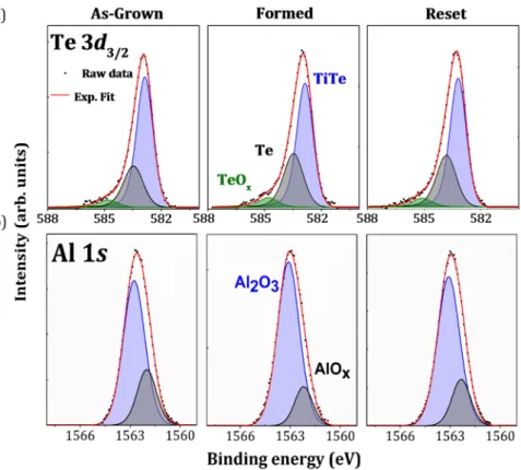
Te and electrolyte chemistry: The Te 3d5/2 core level was not used in our measurements because of the overlap
with the Ta 4s core level. Figure 3(a) shows the Te 3d3/2 spectra. The top electrode is a metallic TiTe alloy but the
Te spectra are asymmetric to higher binding energy, suggesting the possible presence of additional components. There are two possibilities for the HBE components: phase separation with formation of elemental Te (semicon-ductor) and/or oxidation of Te. The spectra have therefore been fitted with three components. The major compo-nent at 582.9 eV is related with the TiTe alloy using simple electronegativity arguments, the second compocompo-nent at 583.6 eV is characteristic of elemental semiconductor Te and the HBE component at 584.9 eV is related to the oxide (TeOx)32,33.
Table 5 shows the relative areas of each contribution in the as-grown, formed and reset spectra. After forming, a decrease in the Ti-Te environment (−7.2%) and an increase in elemental Te (+6.6%) was observed, whereas the reset causes a decrease of elemental Te (−2.7%) and an increase of the Ti-Te bonds (+2.3%). Importantly, both formed and reset samples show evidence for increased TeOx coordination with respect to the pristine sample. This
suggests a non-reversible correlation between the increase in elemental Te and oxygen environment.
The Al 1s core level spectra are shown in Fig. 3(b). The reference spectrum measured outside the top elec-trode on the Al2O3/Ta is shown in Fig. S2(b) of the Supplementary Information. On the basis of the latter, the
Al 1s spectra can be fitted using two components. The two contributions are a sub-oxide (labeled AlOx) at lower
binding energy (BE) of 1561.9 eV and fully oxidized Al2O3 at a BE of 1562.7 eV. The relative areas are reported in
Table 6.
The spectrum measured outside the top electrode (Supplementary Fig. S2(b)) showed the alumina reduction near the Ta bottom electrode, consistent with the presence of a TaOx layer (Fig. S2(a)). Comparison between this
spectrum and that of the as-grown sample showed an increase of the relative AlOx contribution (+16.2%) in the
latter. This result highlights the additional alumina reduction caused by the top electrode deposition. Similar to the case of a ZrTe top electrode9, oxygen scavenging is induced by Ti near the TiTe/Al
2O3 interface. Pumping of
oxygen by the Ti evidenced in Fig. 2b causes the creation of positively charged oxygen vacancies V••
o in the
elec-trolyte. This reduction of the electrolyte may play a significant role in the forming process34–36. Note that oxidation
of the TiTe electrode may also occur through the surface by oxygen insertion in the TaN capping layer. This pro-tective layer is thinned to 5 nm to enable HAXPES analyses of the buried TiTe/Al2O3 and Al2O3/Ta interfaces, may
allow some oxygen transport from atmosphere.
The sub-oxide contribution (AlOx at 1561.9 eV) decreases by 9% relative to the main contribution after
form-ing. This is at first sight surprising since forming involves oxygen migration from top to bottom electrode but may be understood if the diffusion results in oxidation of the Al suboxide at the bottom interface. Conversely,
Ta TaOx or TaN Ta2O5
Al2O3/Ta 74.2 ± 0.2 13.3 ± 0.2 12.5 ± 0.2
As-grown 21.0 ± 0.2 41.0 ± 0.2 38.0 ± 0.2
Formed 14.6 ± 0.2 44.0 ± 0.2 41.4 ± 0.2
Reset 26.7 ± 0.2 39.7 ± 0.2 33.6 ± 0.2
Table 3. Relative areas (%) of the Ta 3d5/2 components measured outside the top electrode and for the as-grown,
formed and reset samples.
TiTe TiOx TiO2
As-grown 32.4 ± 0.1 27.2 ± 0.2 40.4 ± 0.1
Formed 32.5 ± 0.1 36.5 ± 0.2 31.0 ± 0.1
Reset 30.9 ± 0.1 26.5 ± 0.2 42.6 ± 0.1
application of a positive bias voltage to reset the HRS causes an increase of the AlOx contribution (+4.2%) for the
reset state compared with the formed sample, consistent with oxygen transport from the electrolyte towards the top electrode, i.e. oxygen scavenging at the top interface.
The HAXPES analysis at 6.9 keV therefore shows evidence for oxygen migration towards the bottom electrode during forming and concomitant redox reactions at both interfaces.
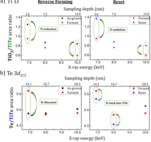
Depth profiles. We have performed the same analysis at 8 and 10 keV photon energy in order to vary the depth
sensitivity (following the IMFP given in Table 1). Figure 4(a) shows the TiO2/TiTe area ratio extracted from the
Ti 1s at 6.9, 8 and 10 keV for the forming and reset steps. During the forming, the TiO2/TiTe area ratio decreases
at all the photon energies, indicating some reduction of the TiOx interfacial layer. This reaction is related to the
oxygen transport towards the alumina and the Ta bottom electrode, resulting in a decrease of the oxygen content in the TiTe layer. The opposite trend is observed for the reset at all the photon energies (increase of the TiO2/
TiTe area ratio), showing the oxidation of TiOx. Oxygen is re-injected in the TiTe layer, under the effect of the
positive bias. Changes are most pronounced at 6.9 keV, i.e. for a measurement more sensitive to the TiTe surface. Figure 3. (a) Te 3d3/2 and (b) Al 1s core level peaks obtained by HAXPES at 6.9 keV on as-grown, formed and
the reset sample of the TaN/TiTe/Al2O3/Ta stack.
TiTe Te TeOx
As-grown 69.1 ± 0.1 26.0 ± 0.3 4.9 ± 0.4
Formed 61.9 ± 0.1 32.6 ± 0.3 5.5 ± 0.4
Reset 64.2 ± 0.1 29.9 ± 0.3 5.9 ± 0.4
Table 5. Relative areas (%) of the Te 3d3/2 components for the as-grown, formed and reset samples.
Al2O3 AlOx
Al2O3/Ta 90.9 ± 0.2 9.1 ± 0.4
As-grown 74.7 ± 0.2 25.3 ± 0.4
Formed 83.7 ± 0.2 16.3 ± 0.4
Reset 79.5 ± 0.2 20.5 ± 0.4
Table 6. Relative areas (%) of the Al 1s components measured outside the top electrode and for the as-grown, formed and reset samples.
The pre-existing TiTe oxidation through the capping layer is another reservoir for oxygen migration in the struc-ture. The TiOx reduction during forming and TiOx oxidation during reset may thus also happen at the TaN/
TiTe interface. We may also consider moisture at the sample surface as further oxygen reservoir. As reported by Tappertzhofen et al.18, OH− ions may be supplied by the water reduction reaction and be injected in the structure
during forming.
The Te/TiTe area ratios are plotted in Fig. 4(b) as a function of photon energy and sampling depth (1.5λ). On forming, the Te contribution is enhanced at 6.9 keV (1.5 λ = 14.1 nm) at the expense of the TiTe component whereas almost no changes are observed at higher energies (8 keV and 10 keV), more sensitive to regions deeper in the stack. Te is liberated in the TiTe electrode and accumulates near the interface with Al2O3. After the reset,
there is a decrease of the Te/TiTe ratio for the lowest photon energies (6.9 keV and 8 keV), most sensitive to the TiTe/Al2O3 interface. We suggest that this may reflect Te partially driven back into the TiTe.
Figure 4. (a) TiO2/TiTe area ratios extracted from the Ti 1s line and (b) Te/TiTe area ratios extracted from Te
3d3/2 measured at 6.9, 8 and 10 keV for as-grown formed and reset samples.
In order to further determine the oxygen depth distribution, ToF-SIMS depth profiling was used. Figure 5 shows the oxygen and tantalum ToF-SIMS profiles in the MCsn+ mode (OCs2+ and TaCs+) for as-grown, formed
and reset samples. The TaCs+ depth profiles (dotted lines) were used in order to guide the eye and define the top
(TaN) and bottom (Ta) electrodes and thus to facilitate the analysis of the oxygen distribution in the stack. The depth profiles for the other elements present in the stack are shown in the Supplementary Information (Fig. S3).
The formed sample depth profile (red line) showed a shift of the oxygen content towards the bottom electrode in comparison to as-grown (black line). This shift is correlated with the HAXPES analysis that shows an oxygen movement from the upper negatively biased electrode towards the bottom electrode driven by the electric field. The variation in the oxygen content is not so pronounced for the reset sample in comparison to formed since the reset process causes smaller changes in the structure than the forming process1,4.
Discussion
Two distinct ion transport mechanisms appear to be at work during the forming and reset stages. The reduction of the pre-existing TiOx layer at the TiTe/Al2O3 interface (see Fig. 4(a)) after forming is correlated with the
varia-tion of the oxygen distribuvaria-tion as a funcvaria-tion of sampling depth, shown in Fig. 5. These results are consistent with an oxygen transport towards the bottom electrode and probably an increase of the V••
o concentration near the
TiTe/Al2O3 interface as shown in Fig. 6. In turn, the oxidation of the alumina layer deduced from the decrease of
the AlOx component after the forming process (− 9%) shown in Fig. 3(b) may be related to the oxidation of the
alumina layer near of the Al2O3/Ta interface caused by the diffusion of O−2 driven by the electric field.
The pre-existing TaOx layer at the bottom electrode was also oxidized during the forming process, acting as
an oxygen getter. Therefore the electrochemical reactions that occurs at each interface, based on these results, can be described as:
At the TiTe/Al2O3 interface:
+ −↔ + −
TiOx 2x e TiOx/2 x/2 O2 (1)
At the Al2O3/Ta interface:
+ −↔ + −
TaOx/2 x/2 O2 TaOx 2x e (2)
The reverse phenomena (TiOx oxidation and TaOx reduction) are observed during the reset, showing oxygen
movement from Al2O3/Ta interface to TiTe layer. During the reset, the alumina is reduced at the Al2O3/Ta bottom
interface due to oxygen migration towards the top electrode whereas oxygen is injected into the interface layer with the TiTe electrode which acts as a getter. The results are consistent with an oxygen transport across the stack, driven by the polarity of the applied bias. They suggest push-pull redox reactions happening at the interfaces with the top and bottom electrodes as a function of bias31. The key point is that the field induces matter transport and
redox reactions at both top and bottom electrode/electrolyte interfaces. Thus, both top and bottom electrode should be considered as active with respect to oxygen transport (getters and reservoirs). These results denotes a pure OXRRAM mechanism with V••
o formation inside of the oxide by oxygen transport. As described by Molas
et al.36, for a Cu-based cell, a pre-forming under negative polarization can be used to improve the RS of a CBRAM
inducing oxygen vacancies in the oxide and facilitating the injection of Cu ions inside the electrolyte during the subsequent cycles of the cell.
A combination of both CBRAM and OxRRAM mechanisms is also possible13,36. The Te/TiTe intensity ratio
analysis is consistent with significant Te release during forming and possible Te diffusion. The intensity ratio sug-gests an accumulation of elemental tellurium at the TiTe/Al2O3 interface after the forming process (see Fig. 4(b)).
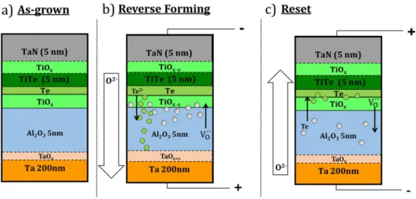
Figure 6. Schematic of the (a) as-grown sample and the redox processes and matter transport taking place during (b) forming and (c) reset in the TaN/TiTe/Al2O3/Ta stack.
Te release was favored by the oxidation of Zr in the case of standard forming of ZrTe-based CBRAMs9. Here,
however, the mechanism may be different because TiOx is reduced at the TiTe/Al2O3 interface because of oxygen
transport during the forming whereas the Ti metal peak intensity is unchanged. The driving force for Te migra-tion might be the electric field, pushing Te2− towards the bottom electrode. Indeed, Te is known to be negatively
ionized in TiTe or ZrTe alloys because of the higher Te electronegativity (2.1) than Ti/Zr (1.6/1.5). This is consist-ent with the increase of Te in the elemconsist-ental form in the Te 3d3/2 spectra and the slight decrease after resetting. Te
which has separated out at the interface or even migrated inside Al2O3 is also more likely to have an environment
including some oxygen atoms, which could well explain the increase in the TeOx component after forming. The
major changes in the Te intensities happen during forming and are not recovered during the reset, evidence that the forming process is not fully reversible and that Te does indeed participate in the resistive switching.
On the basis of these results, we suggest the forming and reset mechanisms which are shown schematically in Fig. 6. The layer structure is only a schematic to allow approximate model calculations of equivalent thicknesses. For example, the interface layer of the top electrode could well be a phase separated TiOx, Te and TiTe. The
effec-tive layer thicknesses calculated here should therefore be treated as (quite good) approximations. To quantify these phenomena, we have used a multilayer model9,37 to study in detail the thickness variation of the elemental
Te and TiO2 layers for as-grown, formed and reset sample (see Supplementary Information Fig. S4 and Table S1).
During forming, we think there is coexistence of interfacial redox processes and localized diffusion mecha-nisms. Redox processes take place at both TiTe/Al2O3 and Al2O3/Ta interfaces. TaOx at the bottom electrode is
oxidized, with a correlated TiOx reduction at the top electrode. These redox processes are activated by oxygen
migration, the O2− ions drifting downwards under the negative bias applied on the top TaN electrode and a
cor-responding increase of the oxygen vacancies concentration at the TiTe/Al2O3 interface. In parallel, the HAXPES
spectra highlight the accumulation of Te at the TiTe/Al2O3 interface. Similarly to oxygen, Te2− might also drift
inside the alumina under the applied field. Considering a hybrid mechanism, a possible physical interpretation of the forming mechanism is thus the coexistence of phenomena typical of both CBRAMs (Te migration) and OXRRAMs (V••
o formation by oxygen transport). Thus, the resistive switching mechanism is possibly related to
the presence of V••
o inside the alumina but also to Te drift12–14. Such hybrid mechanisms have recently been
reported in several papers. Several authors suggest that the formation of metallic filaments is helped by oxygen vacancies, favoring cation insertion inside the electrolyte under bias application18,38. Other studies have
high-lighted conducting paths made by a combination of metallic filaments (Cu, Ag) and oxygen vacancies35,39,40.
The ions and V••
o transport mechanisms are reversed during the reset a) TaOx reduction and TiOx oxidation
following the oxygen movement towards the top electrode, b) less free Te is observed probably because driven back into the top electrode, reforming the TiTe alloy. Both the recombination of oxygen ions with V••
o at the TiTe/
Al2O3 interface by reoxidation and the loss of Te near TiTe might help to switch back the structure in a high
resist-ance state.
This work provides evidence that the OXRRAM mechanism occurs in the TiTe/Al2O3-based CBRAM when a
negative voltage is applied on the device. In addition the results showed a Te release from the top electrode dur-ing the formdur-ing process. Note that the increase of the elemental Te does not necessarily imply migration, it may also be due to the formation of Te-Te bonds inside the top electrode. In this case only the formation of oxygen vacancies inside of the electrolyte then an OXRRAM behavior may explain the resistive switching of the forming process.
Conclusion
In summary, it can be concluded that in the reverse forming of Te-based subquantum CBRAMs the Ta bottom electrode acts as an oxygen getter creating oxygen vacancies at the TiTe/Al2O3 interface. The oxygen movement in
the form of O2− is driven by the electric field from the upper negatively biased electrode towards the bottom one.
Forming also causes an accumulation of elemental Te near the top interface. Te2− might also be pushed inside the
alumina by the electric field. On reset there is a partial recombination of oxygen ions with V••
o near TiTe/Al2O3
interface together with a loss of Te. These results strongly suggest that CBRAM (Te transport) and OxRRAM (V•• o
migration) mechanisms coexist in these Te-based memory cells. Future experiments should include bringing an experimental proof of possible conductive paths in Al2O3 and cycling between set and reset states in order to
study the chemistry of cell endurance.
Data Availability
The datasets generated and/or evaluated during the current study are available from the corresponding author on reasonable request.
References
1. Waser, R., Dittmann, R., Staikov, G. & Szot, K. Redox-Based Resistive Switching Memories - Nanoionic Mechanisms, Prospects and Challenges. Adv. Mater. 21, 2632–2663 (2009).
2. Sawa, A. Resistive switching in transition metal oxides. Mater. Today 11, 28–36 (2008).
3. Ielmini, D. Resistive switching memories based on metal oxides: mechanisms, reliability and scaling. Semicond. Sci. Technol. 31, 063002 (2016).
4. Clima, S. et al. RRAMs based on anionic and cationic switching: a short overview. Phys. Status Solidi RRL – Rapid Res. Lett. 8, 501–511 (2014).
5. Kozicki, M. N. & Barnaby, H. J. Conductive bridging random access memory—materials, devices and applications. Semicond. Sci.
Technol. 31, 113001 (2016).
6. Waser, R. & Aono, M. Nanoionics-based resistive switching memories. Nat. Mater. 6, 833–840 (2007).
7. Calderoni, A., Sills, S., Cardon, C., Faraoni, E. & Ramaswamy, N. Engineering ReRAM for high-density applications. Microelectron.
devices. J. Phys. Appl. Phys. 49 (2016).
17. Wedig, A. et al. Nanoscale cation motion in TaOx, HfOx and TiOx memristive systems. Nat. Nanotechnol. 11, 67–74 (2016). 18. Tappertzhofen, S. et al. Generic Relevance of Counter Charges for Cation-Based Nanoscale Resistive Switching Memories. ACS
Nano 7, 6396–6402 (2013).
19. Arita, M. et al. Microstructural transitions in resistive random access memory composed of molybdenum oxide with copper during switching cycles. Nanoscale 8, 14754–14766 (2016).
20. Fadley, C. S. Hard X-ray Photoemission: An Overview and Future Perspective. In Hard X-ray Photoelectron Spectroscopy (HAXPES) 1–34 (Springer, Cham, 2016).
21. Calka, P. et al. Origin of resistivity change in NiO thin films studied by hard x-ray photoelectron spectroscopy. J. Appl. Phys. 109, 124507 (2011).
22. Bertaud, T. et al. In-operando and non-destructive analysis of the resistive switching in the Ti/HfO2/TiN-based system by hard x-ray photoelectron spectroscopy. Appl. Phys. Lett. 101, 143501 (2012).
23. Sowinska, M. et al. Hard x-ray photoelectron spectroscopy study of the electroforming in Ti/HfO2-based resistive switching structures. Appl. Phys. Lett. 100, 233509 (2012).
24. Cho, D.-Y., Luebben, M., Wiefels, S., Lee, K.-S. & Valov, I. Interfacial Metal-Oxide Interactions in Resistive Switching Memories.
ACS Appl. Mater. Interfaces 9, 19287–19295 (2017).
25. Rueff, J.-P. et al. The GALAXIES beamline at the SOLEIL synchrotron: inelastic X-ray scattering and photoelectron spectroscopy in the hard X-ray range. J. Synchrotron Radiat. 22, 175–179 (2015).
26. Tanuma, S., Powell, C. J. & Penn, D. R. Calculations of electron inelastic mean free paths. V. Data for 14 organic compounds over the 50–2000 eV range. Surf. Interface Anal. 21, 165–176 (1994).
27. Kobayashi, K. Hard X-ray photoemission spectroscopy. Nucl. Instrum. Methods Phys. Res. Sect. Accel. Spectrometers Detect. Assoc.
Equip. 601, 32–47 (2009).
28. Briggs, D. & Seah, M. P. Practical Surface Analysis, Auger and X-ray Photoelectron Spectroscopy. (Wiley, 1996).
29. Doniach, S. & Sunjic, M. Many-electron singularity in X-ray photoemission and X-ray line spectra from metals. J. Phys. C Solid State
Phys. 3, 285 (1970).
30. Takata, Y. et al. Recoil effects of photoelectrons in a solid. Phys. Rev. B 75, 233404 (2007).
31. Bertaud, T. et al. HfO2-based RRAM for Embedded Nonvolatile Memory: From Materials Science to Integrated 1T1R RRAM Arrays. Meet. Abstr. MA2012–02, 2577–2577 (2012).
32. Bahl, M. K., Watson, R. L. & Irgolic, K. J. X‐ray photoemission studies of tellurium and some of its compounds. J. Chem. Phys. 66, 5526–5535 (1977).
33. Neumann, H., Mast, M., Enderlein, J., Tomlinson, R. D. & Yakushev, M. V. XPS Analysis of Bridgman-grown CuInTe2 and of its Native Oxide. Cryst. Res. Technol. 31, 75–85 (1996).
34. Saadi, M. et al. On the mechanisms of cation injection in conducting bridge memories: The case of HfO2 in contact with noble metal anodes (Au, Cu, Ag). J. Appl. Phys. 119, 114501 (2016).
35. Chung, Y.-L. et al. Joint contributions of Ag ions and oxygen vacancies to conducting filament evolution of Ag/TaOx/Pt memory device. J. Appl. Phys. 116, 164502 (2014).
36. Molas, G. et al. Controlling oxygen vacancies in doped oxide based CBRAM for improved memory performances. in 2014 IEEE
International Electron Devices Meeting 6.1.1–6.1.4, https://doi.org/10.1109/IEDM.2014.7046993 (2014).
37. Jablonski, A. & Zemek, J. Overlayer thickness determination by XPS using the multiline approach. Surf. Interface Anal. 41, 193–204 (2009).
38. Valov, I. et al. Atomically controlled electrochemical nucleation at superionic solid electrolyte surfaces. Nat. Mater. 11, 530–535 (2012).
39. Jeon, H. et al. Resistive switching behaviors of Cu/TaOx/TiN device with combined oxygen vacancy/copper conductive filaments.
Curr. Appl. Phys. 15, 1005–1009 (2015).
40. Banerjee, W. et al. Complementary Switching in 3D Resistive Memory Array. Adv. Electron. Mater. 3 (2017).
Acknowledgements
This work was performed on both the CEA Minatec Nanocharacterization Platform (PFNC) and the GALAXIES beamline at SOLEIL Synchrotron, France. The work done at the PFNC was supported by the “Recherche Technologique de Base” program of the French ministry of research.
Author Contributions
M.K.M., E.M., N.B., O.R. and R.G. planned and optimized the experiment(s), M.B. fabricated the investigated samples, M.K.M. analyzed the data and performed the calculations, M.K.M., E.M. and N.B. interpreted the experimental data and prepared the manuscript, M.K.M., E.M., N.B., J.M.A. and J.P.R. participated in the conduction of the HAXPES experiment(s). M.V. performed the ToF-SIMS measurements. All authors discussed the results and commented on the manuscript.
Additional Information
Supplementary information accompanies this paper at https://doi.org/10.1038/s41598-018-36131-7. Competing Interests: The authors declare no competing interests.
Publisher’s note: Springer Nature remains neutral with regard to jurisdictional claims in published maps and institutional affiliations.
Open Access This article is licensed under a Creative Commons Attribution 4.0 International License, which permits use, sharing, adaptation, distribution and reproduction in any medium or format, as long as you give appropriate credit to the original author(s) and the source, provide a link to the Cre-ative Commons license, and indicate if changes were made. The images or other third party material in this article are included in the article’s Creative Commons license, unless indicated otherwise in a credit line to the material. If material is not included in the article’s Creative Commons license and your intended use is not per-mitted by statutory regulation or exceeds the perper-mitted use, you will need to obtain permission directly from the copyright holder. To view a copy of this license, visit http://creativecommons.org/licenses/by/4.0/.