HAL Id: cea-02930899
https://hal-cea.archives-ouvertes.fr/cea-02930899
Submitted on 4 Sep 2020
HAL is a multi-disciplinary open access
archive for the deposit and dissemination of
sci-entific research documents, whether they are
pub-lished or not. The documents may come from
teaching and research institutions in France or
abroad, or from public or private research centers.
L’archive ouverte pluridisciplinaire HAL, est
destinée au dépôt et à la diffusion de documents
scientifiques de niveau recherche, publiés ou non,
émanant des établissements d’enseignement et de
recherche français ou étrangers, des laboratoires
publics ou privés.
Innovative Multilayer OTS Selectors for Performance
Tuning and Improved Reliability
C. Laguna, N. Castellani, M. Bernard, N. Rochat, D. Rouchon, C. Sabbione,
J. Garrione, E. Nolot, G. Bourgeois, M.-C. Cyrille, et al.
To cite this version:
C. Laguna, N. Castellani, M. Bernard, N. Rochat, D. Rouchon, et al.. Innovative Multilayer OTS
Selectors for Performance Tuning and Improved Reliability. IMW 2020 - 2020 IEEE International
Memory Workshop, May 2020, Dresde, Germany. pp.1-4, �10.1109/IMW48823.2020.9108130�.
�cea-02930899�
Innovative Multilayer OTS Selectors for
Performance Tuning and Improved Reliability
C. Laguna
1,2, N. Castellani
1, M. Bernard
1, N. Rochat
1, D. Rouchon
1, C. Sabbione
1,
J. Garrione
1, E. Nolot
1, G. Bourgeois
1, M. C. Cyrille
1, L. Militaru
2, A. Souifi
2,
G. Navarro
1and E. Nowak
11CEA, LETI, MINATEC Campus, 17 rue des Martyrs, 38054 GRENOBLE Cedex 9, France.
2Université de Lyon, INL-UMR CNRS 5270, INSA Lyon, 7 av. Jean Capelle, 69621 VILLEURBANNE, France.
Abstract—In this paper, we investigate an innovative Ovonic
Threshold Switching Selector (OTS) based on Multilayer struc-ture (ML). Thanks to physico-chemical analysis and electrical characterization we show how MLs properties and structure can be tuned thanks to the engineering of each individual layer stoichiometry, thickness and interfaces. Ge/N-doped SbSe-based MLs OTS are analyzed by FTIR and Raman spectroscopy revealing the structural features present in the as-deposited materials and the strong interaction among individual layers at interfaces. We demonstrate the improved variability con-trol of electrical parameters wrt standard OTS achieved by co-sputtering technique, and the high endurance capability of MLs OTS up to more than 2·109 cycles with stable nA leakage current. Moreover, we show how Ge-N bonds play a huge role on OTS thermal stability at 400◦C and how they can be tuned more easily in ML OTS. These developments pave the way towards a new class of OTS materials and their engineering, ensuring high temperature stability and best tuning of electrical performances.
I. INTRODUCTION
Ovonic Threshold Switching technology (OTS), based on amorphous chalcogenide materials, is considered among the most promising Back-End Selector because of its demon-strated reliability in terms of high ON/OFF selectivity, high endurance and high switching speed [1]. Recent developments of OTS materials showed the strong sensitivity of device electrical performance and electrical parameters variability on composition and doping [2]–[4]. This is at the expense of an increased material complexity, dealing with even more of five elements in the same alloy. Moreover, high temperature exposure could induce segregation and crystallization phenom-ena in amorphous chalcogenides, degrading the OTS switching behavior. We showed in a previous work [5] the possibility to combine reliable switching properties and low leakage current introducing a low bandgap As-Te alloy in a high bandgap Se-rich Ge-Se alloy, achieving tunable OTS performances with a relative reduced material complexity, because of the pseudo-binary nature of the fabricated alloy.
In this work, we take advantage of the switching properties of a chalcogenide alloy based on Sb-Se (SS) stacked with Ge layers and selectively doped with N. Thanks to the comparison
We acknowledge the support of European commission, French State and Auvergne-Rhône Alpes region through the funding of ECSEL project WAKEMEUP part of IPCEI (Important project of commun european interest) microelectronics and French Nano2022 program.
SSGN W OTS Bulk W OTS Multilayer TiN TiN ML-A ML-B ML-C 300nm 300nm
Fig. 1.Simplified description of our OTS ML device compared to standard
OTS. The bottom electrode consists in a tungsten plug with a diameter of
∼ 300 nm. A carbon intermediate electrode is fabricated between the top
electrode and the OTS material to prevent intermixing among the two during cycling operations.
of electrical parameters of OTS multilayer structure (ML) with a standard OTS based on a bulk layer (Ge/N-doped SS or SSGN, Fig. 1) designed considering our previous studies on Ge-Se-Sb-N (GSSN) [4], we study the switching performance, the capability to ensure material thermal stability and the endurance in these innovative selectors. Moreover, by physico-chemical analysis we show how ML structure does not depend only on each single layer structure but also on interfaces interactions, leading to a proper control of material properties. This result leads to a lower variability of OTS electrical parameters, shown even after a Back-End-Of-Line-like thermal stress protocol (BEOL). We demonstrate that through an innovative OTS ML based on two different relatively simple alloys, we can target the material stability at high temperatures selectively doping the layers, and tuning the selector switching performances, by properly engineering interfaces, thickness and individual layer stoichiometry.
II. MATERIALCHARACTERIZATION OF
OTS MULTILAYERS
We fabricated OTS MLs by alternative magnetron reactive sputtering from SS and Ge targets doping selectively with N. Three materials were realized with invidual layer thicknesses ranging from 1nm to∼5 nm. The total thickness of the stack is kept constant, therefore the total number of interfaces is higher for thinner layers. We will refer in the following to theses material as ML-A, ML-B and ML-C respectively. SSGN layer was deposited by standard magnetron co-sputtering deposition technique.
We characterize materials using IR spectroscopy. Fig. 2 shows FTIR spectra of SSGN and MLs as deposited and after a
200 400 600 800 1000 N o r m a l i ze d a b so r b a n ce w r t S b -S e p e a k SSGN ML-A ML-B ML-C A s d e p G e -N S u b s t r a t e G e -S e W avenumber (cm -1 ) S b -S e 4 0 0 ° C
Fig. 2. FTIR spectra of SSGN and MLs (top) as deposited and (bottom)
after a 400◦C annealing. The peak at 266 cm−1 corresponds to GeSe4 (ν3
mode) which is priviledged in multilayer structure while the shoulder at
300 cm−1 should correspond to GeSeGe (ν1 mode) [6], [7] that is more
intense in bulk SSGN. After annealing, SSGN bond network evolves to a structure comparable to MLs.
monitored temperature ramp up of 10◦C/min stopped at 400◦C
for ∼1 min. All the spectra are normalized wrt Sb-Se peak as
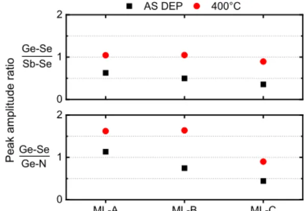
reference. We observe the presence in all the layers of expected Sb-Se and Ge-N bonds. The presence of Ge-Se bonds even in MLs certifies the strong inter-layers interaction and the high probability of Ge-Se formation [7]. Ge-Se bonds are important to preserve the amorphous layer thermal stability and to avoid the OTS mechanism degradation (i.e. layer crystallization). The interfaces in our MLs play the role of controlling such feature, together with SS layer stoichiometry and N doping control. In Fig. 3 this phenomenon is evidenced by the increasing of Ge-Se wrt Sb-Se and Ge-N moving toward a higher interface number in ML-A, even boosted after annealing at 400◦C. Ge-N features in bulk SSGN, important for glass stability, evolves toward a more defined GeN peak [8] that is compatible with the one already present in as-dep MLs, in which it is stable and only slightly increasing after annealing at a higher wavenumber presented in Fig. 2. The higher the content of GeN in the layers, the higher the final thermal stability expected. Selective doping reacheses a higher content of N in SSGN, which explains the higher intensity of Ge-N peak.
Fig. 4 shows Raman spectra for SSGN and MLs as-deposited and after annealing. The major band around 200 cm−1is the convolution of Ge-Se and Sb-Se that is present in both bulk and ML structures. The band near 160 cm−1 can be assigned to vibration mode of a Sb-Sb. In the case of MLs this mode remains stable even after annealing, that could be linked to the structure of SS involving Se2Sb-SbSe2
features [10], [11]. The presence of amorphous Ge layers, and the unchanged MLs associated spectra after annealing, support the integrity of the MLs under thermal stress.
The inter-layers interaction, the stoichioemtry and the selec-tive N doping in Ge+Sb-Se-based OTS MLs lead to a higher control of the material structure and of its thermal stability
AS DEP 400°C 0 1 2 ML-A ML-B ML-C 0 1 2 Sb-Se Ge-Se P e a k a m p l i t u d e r a t i o Ge-N Ge-Se
Fig. 3. Intensity ratios of Ge-Se peaks wrt Sb-Se (top) and wrt Ge-N
peaks (bottom) for ML-A, ML-B and ML-B as deposited and after a 400◦C
annealing, extracted from Fig. 2
100 200 300 400 4 0 0 ° C N o r m a l i z e d R a m a n I n t e n s i t y SSGN ML-A ML-B ML-C a -G e A s d e p S e -S e S b -S e x G e -S e Raman shift (cm -1 ) S b -S b
Fig. 4. Raman spectra for SSGN and MLs as deposited (top) and and
after 400◦C annealing (bottom). All spectra are normalized using the main
feature at 200 cm−1that results from correlation of [SbSe3/2] and [GeSe4/2]
features. Homopolar Sb-Sb bonds are part of the more complex feature
(Se2)Sb(Ge)-Sb(Se2) [10], [11] that stabilizes after annealing.
wrt standard bulk SSGN.
III. ELECTRICALCHARACTERIZATION OF
OTS MULTILAYERSSELECTORS
We performed the electrical characterization of OTS Mul-tilayers analytical selector devices, deposited on a 300 nm W plug. Devices were tested in both quasi-static (DC) and pulsed (AC) mode.
Fig. 5 presents the post-firing DC current-vs-voltage (IV) curves of SSGN and ML-A as an example of the high compatibility of switching behavior between bulk and ML. Leakage current (Ioff) is defined for each material as the current
measured at half of its switching voltage (Vth/2) and Ih is the
holding current.
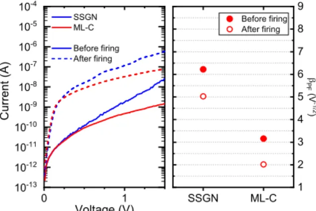
All the experiments were performed on populations of 20 devices. In Fig. 6 we report the subthreshold IV curves before and after firing (DC mode), in order to compare the conduction mechanism in SSGN wrt MLs. Theses curves can be fitted using Poole-Frenkel conduction relation:
ln(I/V )∝ βP F·
√
0 1 2 3 4 10 -13 10 -11 10 -9 10 -7 10 -5 10 -3 C u r r e n t ( A ) Voltage (V) SSGN ML-A V th I h I off @V th /2
Fig. 5.Quasi-static curves for SSGN and ML-A, demonstrating the
compat-ibility of the switching behavior between OTS ML and bulk OTS. We define
the leakage current (Ioff), measured at Vth/2, and the holding current (Ih).
0 1 10 -13 10 -12 10 -11 10 -10 10 -9 10 -8 SSGNML-A ML-B ML-C 1 2 3 4 5 6 7 8 9 C u r r e n t ( A ) Voltage (V) SSGN ML-A ML-B ML-C Before firing After firing b P F ( V -1 / 2 ) Before firing After firing
Fig. 6.Subthreshold IV characteristics before and after firing for SSGN and
MLs (only median curves are shown) (left). Subthreshold conductivity slope
βP F is calculated for all the samples (right).
where βP F parameter reveals the subthreshold dependency
of the layers conductivity, and it is calculated before and after firing. Firing operation induces a material evolution, that appears similar in all the samples. The increase of subthreshold non-linearity is higher in bulk layer wrt MLs samples (i.e. higher βP F) that we think could be correlated with the higher
material disorder after firing operation, already observed in the variability of electrical parameters.
In Fig. 7 and Fig. 8 we report all the electrical parameters measured in AC for the materials investigated, after 104 and
108 cycles. SS shows OTS behavior up to 102 cycles, with
higher dispersion of starting fire voltage (Vfire) and following
Vth, before to trigger crystallization and loss of the OTS
behavior. SSGN presents both higher Vfire and Vthand higher
variability from starting cycles wrt MLs. Lower Vthvariability
in OTS has a strong importance for the reliability of reading operation once co-integrated with resistive memory devices [12]. We think that the gradual reduction of the Vfire from
bulk to MLs can be linked to SS layers thickness. Indeed SS has a lower resistivity [13] compared to N-doped Ge layer and a lower firing voltage wrt to SSGN. Therefore, firing operation
SS SSGN ML-A ML-B ML-C 1 2 3 4 5 6 7 8 9 V o l t a g e ( V ) V fire V th at cycle 10 4 V th at cycle 10 2 V th at cycle 10 8
Fig. 7.Vfireand Vth after 104 and 108 cycles for SSGN and MLs. SSGN
shows higher Vfire and Vth values and higher variability wrt MLs. SS
parameters are shown only up to 102 cycles since after the material triggers
crystallization. SSGN ML-A ML-B ML-C 10 -10 10 -9 10 -8 10 -4 10 -3 C u r r e n t ( A ) I on Cycle 10 4 I h Cycle 10 8 I off
Fig. 8.Electrical parameters Ion, Ihand Ioffafter 104and 108cycles for SSGN
and MLs. Identical results are achieved with both RESET and SET-like pulses conventionally used for Phase-Change Memory applications (not reported for graph clarity).
becomes easier and achieved at lower voltage when SS layer thickness increases.
SSGN shows lower leakage current compared to MLs (Fig. 7), but it confirms the higher variability of both ON (e.g. ON current Ion) and OFF parameters even after 108 cycles.
An Ion/Ioff ratio of more than 106 is ensured in thinnest MLs
with Ioff in nA range with a reduced dispersion.
Endurance capability of OTS ML solution is demonstrated in Fig. 9 where the endurance of ML-A reaches more than 2·109 cycles with extremely low cycle-to-cycle variation of
Ioff and Ion parameters.
In order to evaluate the thermal stability of MLs devices, we annealed the devices with a thermal budget of 30 min at 400◦C. Fig. 10 reports the value of the starting resistance of the devices (Rvirgin), before and after annealing. While ML-A
and ML-B have crystallized, SSGN and ML-C, even if we observe a starting of crystallization, show a totally compatible behavior among selector requirements. The trend is in line with material analyses, where the GeN presence, likely responsible for the glass stability, is found higher in SSGN (Fig. 2). ML-C,
10 1 10 2 10 3 10 4 10 5 10 6 10 7 10 8 10 9 10 -10 10 -9 10 -4 10 -3 10 -2 I on I off C u r r e n t ( A ) Cycles
Fig. 9.Ioffand Ionalong cycling up to 2·109 cycles for ML-A.
SSGN ML-A ML-B ML-C 10 3 10 4 10 5 10 6 10 7 10 8 10 9 10 10 10 11 AS DEP 400°C R vi r g i n ( W )
Fig. 10.Rvirginmeasured at Vth/2 before and after extreme thermal budget of
30 min at 400◦C.
even though its N doping rate is three times inferior to SSGN, shows comparable thermal stability. This result highlights the capability of ML solution to improve the structure control of the layer, in particular enabling selective bonds formation.
Focusing on SSGN and ML-C, Fig. 11 shows their IV curves before and after firing after annealing. The anneal-ing increases significantly the subthreshold conductivity in SSGN wrt ML-C. Moreover, the electric field dependency of subthreshold conductivity remains lower in ML-C (i.e. lower
βP F), confirming a likely lower disorder even after annealing.
Finally, in Fig. 12 we report the post annealing spread in % of Vth and Ioff measured after 104 and 108 cycles for SSGN
and ML-C. Variability of electrical parameters is always lower for ML-C wrt SSGN, even after cycling.
OTS MLs show stable nA range leakage current and high
endurance capability up to more than 2·109 cycles featuring
a huge reduction of electrical parameters variability. Thermal
stability at 400◦C is in line with the one of bulk reference
layer, showing the capability of ML solution to improve the structure control by selective bonds formation.
IV. CONCLUSIONS
We investigated innovative OTS ML selectors based on N-doped Ge and Sb-Se. We showed how the inter-layers
0 1 10 -13 10 -12 10 -11 10 -10 10 -9 10 -8 10 -7 10 -6 10 -5 10 -4 SSGN ML-C 1 2 3 4 5 6 7 8 9 C u r r e n t ( A ) Voltage (V) SSGN ML-C Before firing After firing b P F ( V -1 / 2 ) Before firing After firing
Fig. 11.Subthreshold IV curves before and after firing for SSGN and ML-C
after the 400◦C/30min annealing (only median curves are shown) (left) and
correspondent subthreshold conductivity slope βP F (right).
SSGN ML-C 0 20 40 60 80 100 Cycle 10 4 Cycle 10 8 ( V m a x -V m i n ) / V m e d i a n ( % ) V th I off SSGN ML-C
Fig. 12.Vth(left) and Ioff(right) spread evaluation (in %) after 104and 108
cycles for SSGN and ML-C after 400◦C/30min annealing.
interaction, demonstrated by FTIR and Raman analyses, the stoichioemtry and the selective N doping in our OTS MLs lead to a higher control of the material structure and of its thermal stability. We presented the improved variability control of electrical parameters and high endurance capacity up to 2·109cycles of MLs OTS. Finally, we show how Ge-N bonds
play a huge role on OTS thermal stability at 400◦C and how they can be tuned more easily in ML OTS. We think that these results open to a new class of OTS devices and to their engineering, ensuring high temperature stability and best tuning of electrical performances.
REFERENCES
[1] G. W. Burr et al., J. Vac. Sci. Technol. B, vol. 32(4), pp. 040802, 2014. [2] H. Y. Cheng et al., in Proc. 2017 IEDM, pp. 2.2.1-2.2.4, 2017. [3] D. Garbin et al., in Proc. 2019 IEDM, 35.1.1-35.1.4,2019. [4] A. Verdy et al., in Proc. 2018 IEDM, 37.4.1-37.4.4, 2018. [5] A. Verdy et al., in Proc. IMW 2019,2-4, pp.1-4, 2019. [6] P. Sharma et al., J. Alloys Compd., vol. 480, pp. 934-937, 2009. [7] D.R. Goyal et al., J. Non-Cryst. Solids, vol. 183, pp. 182-185, 1995. [8] A. Verdy et al., in Proc. 2018 IMW, 10.1109, pp. 1-4, 2018. [9] M. Olivier et al., Opt. Express, vol. 4(3), pp. 525-540, 2014. [10] E. Baudet et al., J. Non-Cryst. Solids, vol. 44, pp.64-72, 2016. [11] D. Kau et al, in Proc. 2009 IEDM, 27.1.1-27.1.4, 2009. [12] F.A. El-Salam et al., Vacuum, vol. 44, pp. 1009-1013, 1993.


![[PDF] Support de cours pratique dot Net et ASP - Cours ASP](data:image/gif;base64,R0lGODlhAQABAIAAAP///wAAACH5BAEAAAAALAAAAAABAAEAAAICRAEAOw==)