HAL Id: hal-01764928
https://hal.archives-ouvertes.fr/hal-01764928
Submitted on 5 Jul 2018
HAL is a multi-disciplinary open access
archive for the deposit and dissemination of sci-entific research documents, whether they are pub-lished or not. The documents may come from teaching and research institutions in France or abroad, or from public or private research centers.
L’archive ouverte pluridisciplinaire HAL, est destinée au dépôt et à la diffusion de documents scientifiques de niveau recherche, publiés ou non, émanant des établissements d’enseignement et de recherche français ou étrangers, des laboratoires publics ou privés.
Band Edge Dynamics and Multiexciton Generation in
Narrow Band Gap HgTe Nanocrystals
Clément Livache, Nicolas Goubet, Bertille Martinez, Amardeep Jagtap,
Junling Qu, Sandrine Ithurria, Mathieu Silly, Benoit Dubertret, Emmanuel
Lhuillier
To cite this version:
Clément Livache, Nicolas Goubet, Bertille Martinez, Amardeep Jagtap, Junling Qu, et al.. Band Edge Dynamics and Multiexciton Generation in Narrow Band Gap HgTe Nanocrystals. ACS Applied Materials & Interfaces, Washington, D.C. : American Chemical Society, 2018, 10 (14), pp.11880-11887. �10.1021/acsami.8b00153�. �hal-01764928�
1
Band Edge Dynamics and Multiexciton Generation in Narrow Band Gap HgTe Nanocrystals
Clément Livache
1,2, Nicolas Goubet
1,2, Bertille Martinez
1,2, Amardeep Jagtap,
1Junling Qu,
1Sandrine Ithurria
2, Mathieu G. Silly
3, Benoit Dubertret
2, Emmanuel Lhuillier
1*1
Sorbonne Universités, UPMC Univ. Paris 06, CNRS-UMR 7588, Institut des NanoSciences de
Paris, 4 place Jussieu, 75005 Paris, France
2
Laboratoire de Physique et d’Etude des Matériaux, ESPCI-ParisTech, PSL Research University,
Sorbonne Université UPMC Univ Paris 06, CNRS, 10 rue Vauquelin 75005 Paris, France.
3
Synchrotron-SOLEIL, Saint-Aubin, BP48, F91192 Gif sur Yvette Cedex, France
Abstract: Mercury chalcogenide nanocrystals and especially HgTe appear as an interesting platform for the design of
low cost mid infrared (mid-IR) detectors. Nevertheless, their electronic structure and transport properties remain poorly understood and some critical aspects such as the carrier relaxation dynamics at the band edge have been pushed under the rug. Some of the previous reports on dynamics are setup limited and all of them have been obtained using photon energy far above the band edge. These observations raise two main questions: (i) what are the carrier dynamics at the band edge and (ii) should we expect some additional effect (multiexciton generation or MEG) as such narrow band gap materials are excited far above the band edge? To answer these questions, we developed a high bandwidth setup which allows us to understand and compare the carrier dynamics resonantly pumped at the band edge in the mid-IR and far above the band edge. We demonstrate that fast (>50 MHz) photoresponse can be obtained even in the mid-IR and that MEG is occurring in HgTe nanocrystal arrays with a threshold around three times the band edge energy. Furthermore the photoresponse can be effectively tuned in magnitude and sign using a phototransistor configuration.
Keywords: HgTe, narrow band gap nanocrystals, mid infrared, band edge dynamics, multi-exciton generation, ,
photodetection.
2
INTRODUCTION
Nanocrystals are promising building blocks for the design of low cost and high performance optoelectronic devices,1 spanning from light emitting diodes,2 lasers,3–5 solar cells6,7 and more recently infrared (IR) photodetectors.8,9 The field of IR photodetection remains led by epitaxially-grown semiconductors made of II-VI (HgCdTe) and III-V (InSb, InGaAs) materials and their heterostructures (GaAs/AlGaAs). However, the cost of such technologies remains prohibitive and limits the use of IR camera to niche markets such as defense and astronomy. Expansion of IR camera to a mass market scale requires a severe cost disruption which is unlikely to result from historical technologies.10 Nanocrystals appear as an interesting alternative which may bridge the gap between expensive high cost, high performances photon detectors and the low cost, lower performances thermal detectors.
Among potential candidates to address the mid-infrared range of wavelengths, mercury chalcogenides (HgX) are by far the most advanced material to tackle this challenge.11–14 HgX colloidal quantum dots (CQDs) combine a tunable absorption from the visible range up to the THz range15 with photoconductive properties.16 While intraband transition (as in HgSe or HgS) appears as an emerging path for the design of CQDs based IR photodetector,15,17 their overall level of performance remains weaker that the one of interband systems based on HgTe.8Moreover, HgTe CQDs benefit from their proximity with the HgCdTe alloy in terms of electronic structure knowledge and material processing. In spite of recent impressive progresses such as the development of multispectral detectors,18,19 the report of first photovoltaic device based on HgTe CQDs20, the coupling to plasmonic structures to enhance the photoresponse21,22 or tune the spectral response23, some central questions are still unaddressed. Among them, the question of the carrier dynamics at the (narrow) band edge remains open. From an applied perspective, this question is of utmost interest since it relates to the detection bandwidth. Overall, detectors based on HgTe CQDs have been reported to be fast detectors with a µs to ms time response.24,25 Nevertheless, in most of the reports the probed dynamics are setup-limited or, even worse, dynamics are probed using photon energies far above the band edge, typically using pulsed lasers and diodes in the visible21 and near IR.20 These observations raise two main questions: (i) what are the carrier dynamics at the band edge in narrow band gap nanocrystals or, in engineer words, how fast is the mid-IR bandwidth? and (ii) should we expect some additional effect (multiexciton generation (MEG), hot electrons…) as such narrow band gap CQDs are excited far above the band edge?
Investigating the dynamics in mid-IR nanocrystals is especially challenging. Time resolved spectroscopic methods such as time resolved photoluminescence (PL), transient absorption and ultrafast pump-probe experiments are widely used in the visible range to probe a wide range of effects in nanocrystals such as hot exciton relaxation or MEG26,27. However, their use in the mid IR faces two main difficulties which are the intrinsically low PL efficiency of IR emitters and the lower efficiency of IR setup (less efficient power sources and detectors). As a result, new approaches have to be developed. Recently Livache et al reported time resolved photoemission as a possible alternative path to probe carrier dynamics in near IR HgTe nanoplatelets.28 In this article we have used a nanosecond (ns) pulsed, high power density quantum cascade laser (QCL) to probe the carriers dynamics almost resonantly with the band edge. We demonstrate that band edge relaxation is faster than 10 ns, which is promising for the design of very high bandwidth setup based on colloidal nanocrystal including in the mid IR range.
Moreover, with their extremely small band gap (270meV), HgTe CQDs are an interesting platform for the investigation of MEG/hot electron effects in nanocrystals. We consequently expand the investigation of the carrier dynamics while the CQDs are excited far (up to six time) above the band edge energy. We reveal that (i) MEG occurs in such QD at a threshold which is around 3 times the band edge and (ii) thanks to a large bandwidth setup, phototransport occurs via multiple trapping transport which can be used to estimate the sub band gap density of state.
Finally, in the last part of the paper, we demonstrate that the photoresponse of such CQDs can be fully controlled by the addition of a gate. Device performances can be improved thanks to the control of carrier density: photoresponse
3
increases under holes injection and decreases under electrons injection, up to the point that the sign of the photoresponse can even be tuned.
4
METHODS Chemicals
Mercury chloride (HgCl2, Strem Chemicals, 99%), tellurium powder (Te, Sigma-Aldrich, 99.99%), trioctylphosphine (TOP, Cytek, 90%), oleylamine (Acros, 80-90%), dodecanethiol (DDT, Sigma-Aldrich, 98%), 1,2,ethanedithiol (EDT, Fluka, 98.0%), hydrochloric acid (HCl, Mieuxa, 25%), lithium perchlorate (LiClO4, Sigma-Aldrich, 98%), polyethylene glycol (PEG, Mw = 6kg.mol-1), chloroform (Carlo Erba), ethanol absolute anhydrous (Carlo Erba, 99.9%), methanol (Carlo Erba, 99.8%), acetone (Carlo Erba, 99.8%), n-hexane (Carlo Erba), n-octane (SDS, 99%), toluene (Carlo Erba, 99.3%),. All chemical are used as received, except oleylamine which is centrifuged before used. Mercury compounds
are highly toxic. Handle them with special care.
HgTe QDs synthesis
HgTe quantum dots with band edge cutoff around 2000 cm-1 are synthesized with a modified protocol from the reference.29 27 mg of HgCl
2 and 10 mL of oleylamine are degassed under vacuum at 120°C in a 50 mL three-neck flask. A pre-heated solution made of 100 µL of TOP:Te and 9.9 mL of oleylamine is injected into the flask. One has to note that pre-heating is essential to synthesize nanocrystals with low size dispersion. The solution color quickly changes from light yellow to dark-brown. After 3 min, the reaction is quenched with an injection of a solution of 1 mL of dodecanethiol and 9 mL of toluene. The temperature quickly drops to 70-80°C. Resulting solution is precipitated with addition of 90 mL ethanol and then centrifuged. The precipitate is redispersed in chloroform and four drops of dodecanethiol are added. A second washing step is carried out with 80 mL of methanol. The stability of the final colloidal solution is improved by redispersing the nanocrystals in chloroform.
Au/Glass electrodes fabrication
Microscope glass slides cut in half are cleaned by sonication in acetone and rinsed with isopropanol, then receive a 5 min oxygen plasma cleaning. An adhesion primer (TI-PRIME) is spin-coated onto each substrate before AZ5214E resist is spin-coated and baked at 110°C for 90s. A MJB4 mask aligner is used to expose the substrates to UV light for 2 s through a lithography mask. Black paper is put under the glass slides to prevent light from being reflected back to the resist. Substrates are then baked at 125°C for 2 min to invert the resist and flood-exposed for 15 s with the mask aligner, again using black paper. Resist is developed using AZ326 developer for 20 s and rinsed with pure water. Patterned substrates are dried and cleaned with 5 min of oxygen plasma to remove resist residues. In a thermal evaporator, 5 nm of chromium are deposited as an adhesion promoter before 80 nm of gold are evaporated. Lift-off is conducted in an acetone bath for at least one hour. Electrodes are 2.5 mm long and spaced by 20 µm.
PET/ITO electrodes
A PET/ITO wafer is cleaned using acetone and isopropanol. AZ5214E resist is spin-coated and baked at 110°C for 90s. Substrates are exposed to UV light for 4 s through a mask, then dipped into a AZ326 developer bath. Electrodes are then etched using 25% HCl for 10 s and rinsed with pure water. Electrodes are 1 mm long and spaced by 20 µm.
Electrolyte preparation
In our top-gated FET geometry, we use a quasi-solid electrolyte prepared as follows. In a glove box, 0.5 g of LiClO4 are mixed with 2.3 g of PEG (MW = 6 kg.mol-1). The resulting mix is heated at 170°C for 2 h until the solution turns transparent.
5
In a nitrogen-filled glove-box, pre-patterned interdigitated gold electrodes (20 digits, 20 µm separation) on glass substrate are dipped in a solution of HgTe QDs in chloroform. The substrate is tilted to allow the excess solution to drip, ensuring a smooth and homogenous coating. Ligand exchange is performed by dipping the film in a ethanedithiol (EDT) solution in ethanol (1% w/) for 90 seconds and rinsing it in pure ethanol for 30 seconds. This process is repeated 3 times to fill the cracks and reach a device resistance of 10 to 40 kΩ.
FET device preparation and measurements
First, a regular device is prepared in air-free conditions using the protocol described above. An electrolyte (PEG 6k + LiClO4) is heated at 90°C and brushed atop of the device and allowed to solidify in the glove-box for two hours. Drain, source and gate electrodes are then connected to the outputs of a Keithley 2634b dual-channel source-meter controlled by a LabView software. Transfer curves are acquired by setting the drain voltage to 100 mV and sweeping the gate voltage at a 10 mV/s rate. Both drain and gate currents are monitored and the full cycle is repeated 2 times to ensure stable operation.
I-T curves under dark condition
The sample is connected in an closed-cycle cryostat and biased under 1 V by a Keithley 2634 source-meter. The sample is cooled down from 300 K to 15 K while current and temperature are measured every 200 ms.
Temperature-resolved CW measurements
The sample is connected in a cryostat and biased (1 V) using a Keithley 2634b source-meter. Illumination is provided through a glass window by 4.4 µm QCL. The transparency of the glass window for MIR pulses is around 30% and is accounted for in the presented data. Data are acquired using the Keithley 2634b source-meter through a homemade LabView program.
GHz time-resolved photocurrent measurements in the MIR
The sample is connected in a cryostat (for temperature-resolved measurements) or in an open sample holder, and biased using a 9 V battery. Illumination is provided by 20 to 500 ns pulses from a 4.4 µm QCL laser (MirSense) operated at 200 kHz. Transient photocurrent is acquired using a 50 Ω-6 dB attenuator load, fed into a FEMTO-DUPVA GHz amplifier and visualized on either a Tektronix 350 MHz oscilloscope or a 12 GHz sampling oscilloscope (PicoScope) depending of the desired bandwith.
GHz time-resolved measurements at 355 nm
1 ns, 70 µJ pulses at a repetition rate of 100 Hz are produced by a Crylas FTSS 355-80 laser. The beam is separated to illuminate both a photodiode (trigger signal) and the sample. The sample (on PET/ITO substrate) is kept under vacuum and connected to a Keithley 2634b source-meter. A bias of 10 V is applied and the signal is acquired through a 50 Ω load on an oscilloscope (Rohde & Schwarz, RTE 1102).
kHz photoresponse measurements
The sample is connected in a cryostat and biased (1 V) using a Keithley 2634b source-meter. Illumination is either provided by a 4.4 µm QCL laser, a 1550 nm laser diode (Thorlabs FPL1055T) or a 808 nm laser diode (OdicForce RLD808300). The light beam is mechanically chopped using a Thorlabs MC2000B optical-chopper with MC1F10 blade set to 1 kHz. Current from the sample is amplified using a FEMTO DLCPA-200 current amplifier with matched bandwidth and fed into a 350 MHz oscilloscope. Beam powers, beam sizes, transparency of cryostat window as well as relative absorptions are accounted for in the presented data.
6
The sample is connected in a cryostat, biased (1 V) by a Keithley 2634b and illumination is provided by one of the three lasers. For MIR QCL, frequency is set by optically chopping the beam between 1 Hz and 1 kHz and triggering on single pulses for frequencies above 1 MHz. For laser diodes at 808 nm and 1550 nm, electrical chopping allows their modulation from 1 Hz to 40 kHz. Acquisition bandwith-matched:
- the Keithley source-meter through a labview program when the modulation is slower than 1 Hz; - an oscilloscope through a DLCPA-200 current amplifier between 1 Hz and 100 kHz;
- an oscilloscope through a 50 Ω load and a FEMTO DUPVA GHz voltage amplifier above 100 kHz.
CW measurements under gate bias
The sample is connected in an open setup with a hole allowing back-side illumination of the sample through the glass substrate. Illumination is provided by a 808 nm laser. Drain and gate voltages are controlled by a 2-channels Keithley 2634a source-meter. Drain voltage is set to 100 mV and gate voltage is swept from -2 to 2 V. For each 200 meV gate voltage step, drain current is allowed to stabilize for 3 minutes and is then acquired for 10 seconds in the dark, followed by 10 s of illumination and 60 seconds of dark.
7
DISCUSSION
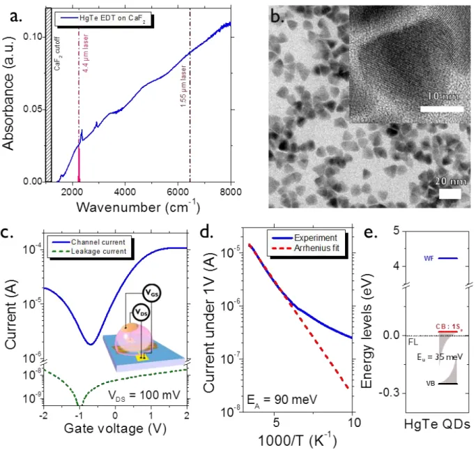
HgTe CQDs have been synthetized according to the Keuleyan’s methods29,30 and present a band-edge energy at 2200 cm-1 (≈4.5 µm or 270 meV) with a cut-off at 1800 cm-1, see Figure 1a. Such transition energy has been chosen to absorb the pulsed QCL (2250 cm-1 or 4.4 µm) which will be used to probe the band edge dynamics. Note that the IR spectrum does not reveal the presence of any longer wavelength absorption relative to intraband feature (see Figure S1 of the SI). These CQDs present a typical 12-15 nm edge size as revealed by the transmission electron microscopy, see Figure 1b. They are crystalline (see inset of Figure 1b) with a zinc blende structure.24
Figure 1:Physical properties of HgTe QDs used in this work. a. FTIR spectrum of EDT-capped HgTe QDs assembled into a film on CaF2 substrate.
Colored lines indicate the energy of two IR laser sources used in the work. b. TEM image of HgTe QDs. Inset: High-resolution TEM image of a single QD. c. Transfer curve (drain current as a function of gate bias) of EDT-capped HgTe QDs sample using electrolytic gating. The curve shows ambipolar behavior. Inset: scheme of the FET device. d. Cooling curve of an EDT-capped HgTe QDs sample under 1V bias. The Arrhenius fit gives a value of 90 meV for activation energy. e. Energy levels of HgTe QDs determined using XPS, with Urbach tails describing the trap distributions.
Before investigating the carrier dynamics, it is critical to further clarify their electronic spectrum and transport properties. After synthesis, CQDs are capped with insulating organic ligand (dodecanethiol, DDT). To make the CQD array conductive and strengthen the inter-dot coupling, ligand exchange is carried out by replacing dodecanethiol ligands by ethanedithiol (EDT). The film is deposited on pre-patterned Au interdigitated electrodes and an ion gel electrolyte is added as a gate, see the inset of Figure 1c for a scheme of the device. Electrolyte gating ensures a strong tunability of the carrier density, air operability31 and also allows to gate thick film (100 nm in our case) which is critical for the design of phototransistors.18Erreur ! Signet non défini. The transfer curve (drain current vs gate bias) reveals
8
an ambipolar behavior where both hole and electron conductions are observed, see Figure 1c. The electron mobility is nevertheless an order of magnitude higher than the one from the hole. Moreover, the charge neutrality point is clearly shifted toward negative biases (around -600 meV), which suggests an n doping. The temperature dependence of the film conductance is given in Figure 1d and follows an Arrhenius law close to room temperature, with an activation energy of 90 meV. This value is slightly lower than the half band gap value (120 meV) expected for an intrinsic semiconductor material and further suggests the lightly doped character of these CQDs. Using photoemission, conducted on the TEMPO beamline of synchrotron Soleil, we are able to reconstruct the electronic spectrum of 5 µm band edge HgTe CQDs in absolute energy scale (Figure 1e), see SI for data acquisition and processing protocol. The work function of the material has been estimated to be 4.23 eV and the Fermi level lies just below the conduction band. This observation revealed that the doping observed using transport measurement is due to electrons. The Fermi level remains nevertheless within the gap which is consistent with the lack of intraband feature in the absorption spectrum and recent observations from the literature.32,33 Noise characteristics and detectivity have already been demonstrated24 in the same kind of EDT-capped HgTe CDQs, this is why we focus on probing photoconductivity dynamics to get a deeper understanding of the material properties.
Thanks to this understanding of the electronic structure, we can now investigate the photoconductive properties of the narrow band gap HgTe while resonantly exciting the interband transistion. To do so, we use a specially designed short-pulsed (6 ns rise time) and high power (up to 100 mW) QCL operating at 4.4 µm (2200 cm-1 or 280 meV) from MirSense. The latter allows operation both in continuous wave (CW) and pulsed mode. The QCL light is shined on the sample mounted in a cryostat, see Figure 2a for a scheme of the setup. To prevent any heating of the sample and also to accurately extract the photocurrent in spite of the low signal to noise ratio, the measurement is conducted while the light is modulated by an optical chopper. We can then follow the temperature dependence of the dark and photocurrent, see Figure 2b. The dark current decreases as temperature is reduced according to the reduction of the thermally activated carriers previously observed in Figure 1d. The photocurrent shows a similar trend, with nevertheless a smaller activation energy, which we can attribute to the thermal activation of the mobility occurring in hopping transport.34 Under such illumination power density (0.37 W.cm-2), the background limited performance (BLIP) temperature, defined as the temperature where the photocurrent equals the dark current is estimated to be 78 K.
9
Figure 2: a. Scheme of the measurement setup with a mid-infrared QCL. b. Evolution of the current in the dark and under MIR illumination as
the sample is cooled. Inset: evolution of the modulation with temperature. c. Typical sample response to a laser-limited 20 ns QCL pulse in the MIR. Inset: response to a 500 ns QCL pulse allowing the extraction of rise and fall time constants of the sample: trise = 23 ns and tfall = 15 ns. QCL
power is 0.6 W/cm² and bias is 9 V. d. Sample response to a 1 ns, high energy pulse in the UV (355 nm), as a function of optical power. The two components are fitted to extract recombination time and Urbach energy.
We now want to probe the dynamics of the photoresponse at high frequency and at the band-edge. The signal is acquired through a 50 Ω resistor before being amplified with a GHz-bandwidth voltage amplifier (see Figure S4 of the SI for more details). The inset of Figure 2c presents the typical photocurrent response of the HgTe CQDs film to two different pulsewidths in the MIR. The 500 ns pulse is almost perfectly imaged by the sample, with rising and falling times of 23 and 14 ns, respectively. Those values are in the range of specifications of our laser, which is supposed to have 6 ns rise/fall time. A laser-limited 20 ns pulse (see Figure 2c) is still reproduced by our detector, with the rising part of the response corresponding to the duration of the pulse. This fast photoresponse is a strinking difference with other nanocrystals based technology being able to address the 3-5µm range of wavelength. Typically HgSe nanocrystals, which rely on intraband transition present a slow photoresponse with a 3dB frequency around 50Hz.15,35
From this data, we can conclude that the cut-off frequency of our device is extremely high (50 MHz) even while exciting the system in the mid IR.
10
For the sake of comparison we also investigate the carrier dynamics while the sample is excited far above the band edge. In this case, we use a 355 nm ns-pulsed laser source with a high power density, as recently described in ref36, also see Figure S4 for a scheme of the setup. Thanks to the low repetition rate and high power density of the laser, this setup presents both a large temporal (6 orders of magnitude) and intensity range of response (>3 decades). The photoresponse of the HgTe film to such short and high energy pulse is shown in Figure 2d. At early time, there is a first rise which follows the pulse duration. The decay is then composed of two parts. Up to 10 ns, we observe an exponential decay which is followed at longer time scale (from 10 ns to 10 µs) by a power law decay.
The fast initial decay presents a characteristic time constant of 1.2 ns, This time scale is typically shorter than the hopping time which is given by
T
µk
eR
b hop3
2
2
, with e the proton charge, R (≈6 nm) the nanoparticle radius, µ the mobility, kb the Boltzmann constant and T the temperature (300 K). Assuming a mobility of 10-3 cm2V-1s-1 from previous report,14 we estimate the hoppingtime to be ≈10 ns. According to Gao et al,37,38 at such early time scale, only the intradot carrier density relaxation is probed. The measured currents below this hopping limit result from displacement currents due to the variations of the electrical field and the effective medium dielectric constant while the carrier density is changed.39 Thus this early relaxation leads to a decay time which is similar to the one expected for PL of HgTe CQD with a 5 µm cut off wavelength, while the time resolved PL is almost impossible to obtain given the quasi null PL efficiency. At longer time scale, typically after a few hopping timescale, the transport can induce some inter dot change of the carrier density and filling of the surface traps. The power law observed in the transient photocurrent is characteristic of a multiple trapping transport mechanism.40,41 We recently detailed that this regime can be used to estimate the distribution of state within the gap, given by the Urbach energy42 (U
E
) according to the equationb
T
k
E
b U
1
where b is the exponent obtained from the power law fit of the transient photocurrent at long(>10 ns) time scale. In the case of EDT we obtain a value of 36±1 meV for the Urbach energy. It is also worth noting that the multiple trapping regime is only revealed under strong excitation and that lower power density mostly exhibit the early intradot relaxation, indicating that trap filling might be power-dependent. Thanks to this understanding we can come back to the band edge dynamics. In spite of its “high power density” the QCL source operates in low energy density compared to the UV laser (1019 photons/s for QCL vs 1021 photons/s for 1.6 µJ pulse of UV laser), hence we do not observe any long-lived signature of trapping but only the fast, early decay. According to Figure 2d, the multitrapping regime appears at longer time scale when the light irradiance is increased, thus the fast dynamics observed at the band edge is due to the intradot carrier recombination which is much faster than the detrapping processes. Eventually, ratio of dynamics for the two processes (recombination vs trapping) makes the usual slowering of the photoresponse resulting from trapping quite ineffective in HgTe narrow band gap nanocrystals. This suggests that the time response of the HgTe CQD film can potentially be reduced to time scales as short as ≈1 ns.
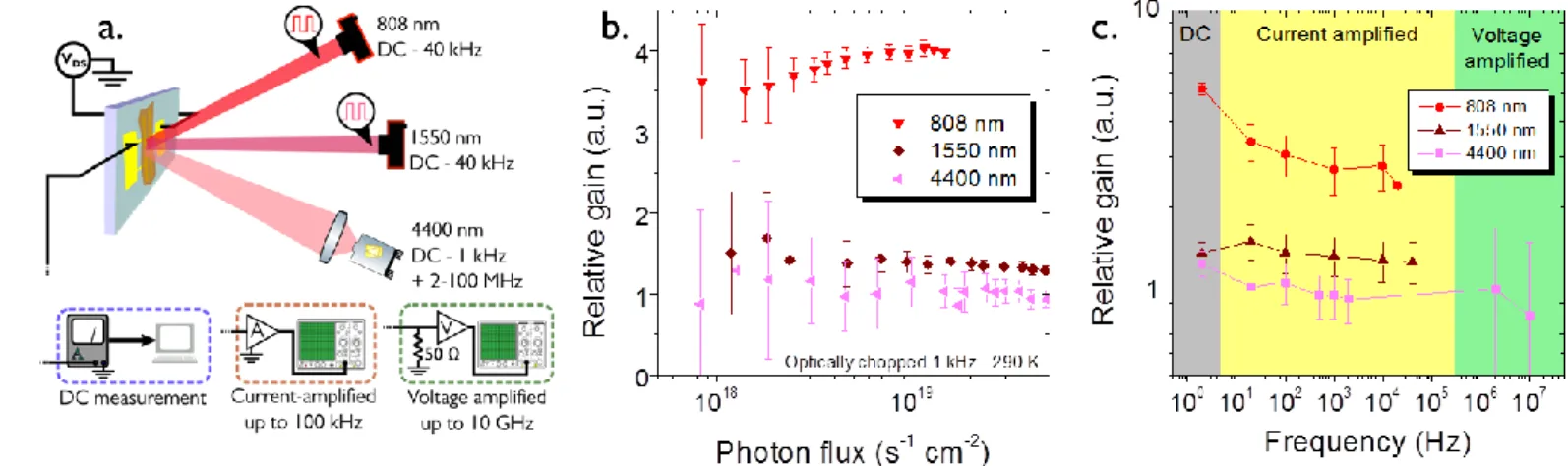
Because of their narrow band gap nature (270 meV), these HgTe CQDs are a promising platform for the investigation of MEG since it is relatively easy to excite them far above the band edge.43 Moreover as opposed to PbS44,45 there are only few reports on MEG in Hg(Cd)Te QD,46,47 while this material may present a threshold for MEG as low as two band edge energy due to relatively large ratio of the hole mass over the electron mass.48 Here we choose to investigate the MEG effect while shining laser sources at the 1.03 x EG (QCL at λ=4.4 µm), ≈3 x EG (laser diode at λ=1.55 µm) and 5.7 x EG (laser diode at λ=808 nm), EG being the band edge energy. Figure 3a gives a scheme of the setup with the three different sources. Because the experimental observation of MEG has led to a lot of controversy in the past,48 we have carefully checked several points. First, the measurements are conducted at low pumping
11
fluence. Indeed, considering an absorption cross section per QD49 of σ
QD = 6x10-15 cm² at 5 µm, we can write the number of excitons per QD as 𝑛𝑒𝑥= 𝜎𝑄𝐷∙ 𝜙 ∙ 𝜏𝑒𝑥𝑐 with 𝜙 the incident photon flux and 𝜏𝑒𝑥 the exciton lifetime.
Taking a value of 1019 s-1cm-2 for the photon flux and a conservative assumption of 10 ns for the lifetime, we get 𝑛𝑒𝑥= 6𝑥10−5 exciton/QD, far below 1. We can hence rule out any effect of multi-excitons injection in this regime.
Moreover, measurements are conducted with modulated light in a lock-in detection configuration, and in particular DC measurements will be excluded because they include some drift of the signal due to heating. Finally using frequency resolved measurements, we check that the responsivity of our device is frequency independent over a broad range (10 Hz-10 kHz). We can thus exclude that the difference of behavior with photon energy may result from frequency dependence of the signal. Moreover the flatness of the photoresponse with frequency (see Figure
3c) is of utmost interest for the future use of the material for photodetection since it limits the drift and potential
needs for a two point recalibration.
Figure 3: Multi-exciton generation in EDT-capped HgTe QD films. a. Scheme of the high-bandwidth measurement setup using alternatively
three different laser sources ranging from NIR to MIR. Acquisition can be changed to be bandwidth-matched. b. Relative gain 𝒈 = 𝑰𝒑𝒉/𝜼𝒆𝝓𝟎
(expression is described in text) as a function of photon flux for the three different wavelengths. For the three lasers, the beam is chopped at 1 kHz using an optical chopper and the sample is biased at 1 V. c. Frequency dependence of the relative gain for the three wavelengths. Frequency ranges from DC to 10 MHz and response is measured with bandwidth-matched acquisition setup. Sample bias is 1 V and the experiment is conducted at room-temperature.
As an intrinsic efficiency parameter, we choose to plot the relative gain. The gain is defined as 𝑔 =𝑅∗ℎ𝜈
𝑒𝜂𝜆 with 𝑅 =
𝐼𝑝ℎ
𝑃𝑜𝑝𝑡 the sample responsivity (ratio of photocurrent over incident light power), ℎ𝜈 the photon energy, e the
elementary charge and 𝜂𝜆= 𝛼𝜆
𝛼4400𝑛𝑚 the ratio of absorption of the QD film at the wavelength 𝜆 by the absorption at
4400 nm.50 Written as a function of photon flux 𝜙, this intrinsic gain becomes 𝑔 = 𝐼𝑝ℎ
𝑒𝜂𝜆
1
𝜙. We would like to point that
we do not present here absolute values for intrinsic efficiencies, as everything is normalized to the value measured for illumination at 4.4 µm. Figure 3b presents the evolution of the relative gain 𝑔𝜆/𝑔𝑀𝐼𝑅 with photon flux for the
three different wavelengths. In this experiment, all lasers are optically chopped at 1 kHz and the photon flux is changed by adjusting the beam power. It appears that illuminations at 4400 nm and 1550 nm have very similar efficiencies, when the 808 nm illumination shows a 3 to 4 times higher efficiency. We have here a manifestation of the MEG effect, with a photon energy threshold of at least 3 x EG since this effect is barely observed for 1550 nm illumination. This value is slightly above the value of 2.5 x EG determined by spectroscopy means on more confined HgTe QDs by Al-Otaify et al.47 Our observation consequently also suggests that many reports of the quantum efficiency and photoresponse of device based on narrow band gap CQD and probed with wavelength far above the band edge may overestimate the final device performance in the mid-IR.
12
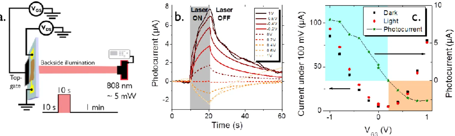
In the last section of this paper, we investigate the tunability of the photoresponse under Fermi level control as a path to tune the majority carrier density18,25,28 and a way to reduce dark current.12 A scheme of the setup is given in
Figure 4a. As the gate bias is applied, see Figure 4b, not only the magnitude of the response can be tuned but even
its sign. Overall positive photoresponse is obtained under hole injection (negative gate bias), while the photoresponse turns negative under electron injection (positive gate bias), see Figure 4b and c. Such negative photoresponse has already been observed in CQDs film,51 Si nanowires52 or Van der Waals heterostructures53 and explained by Rose.54
Figure 4: Negative photocurrent behavior under gate bias. a. Scheme of the experiment: the sample with an electrolytic gate is illuminated
from the back with an 808 nm laser. b. Photocurrent response of the sample to a 10 s light pulse as a function of gate bias. Drain bias is set to 100 mV and gate bias is swept from -1 V to 1 V. c. Reconstructed transfer curve (channel current as a function of gate bias) and photocurrent maximum intensity as a function of gate bias.
To clarify this observation we propose the following model. Let us consider that the current density through our films can be written 𝑗 = 𝑒(𝑛𝑒𝜇𝑒+ 𝑛ℎ𝜇ℎ)𝐸, with ne, µe, nh, µh the electrons (resp. holes) densities and mobilities in the conduction band (resp. valence band), e the elementary charge and E the applied drain source electric field. Our system is initially electron-rich (Figure 1e), so we can set the hole density to 0 as long as we do not consider too negative gate biases. Under hole injection, since the Fermi level is more deeply within the band gap, we have 𝑛𝑑𝑎𝑟𝑘+ Δ𝑛𝑔𝑎𝑡𝑒 ≈ 0, making this regime the most interesting for photodetection. The light illumination induces a
strong change of the carrier density leading to a strong positive photoresponse. Because of the ambipolar behavior of our material, dark current also increases under hole injection and the Ilight/Idark ratio shows a maximum value around a gate bias of -600 mV (see Figure S7). It is interesting to note that this value corresponds to the charge neutrality point determined in Figure 1c, and that it gives us information about the leverage we get using this electrolytic gate. Assuming that this gate bias corresponds to the point where the Fermi level lies in the middle of the gap and knowing from Figure 1e that there is 120 meV between the Fermi level at zero gate bias and the middle of the gap, we get a value of Δ𝐸𝐹
Δ𝑉𝐺𝑆 = 0.2. While this value is smaller than the value of 1 obtained using a four
electrodes electrochemistry setup, it still enables the probing of large energy scales with small applied voltages. Under electron injection though, the Fermi level is within the conduction band and the nanocrystals get degenerately doped. The electron density is large and set by the gate rather than by the light. This leads to 𝑛𝑒=
𝑛𝑑𝑎𝑟𝑘+ Δ𝑛𝑔𝑎𝑡𝑒+ Δ𝑛𝑙𝑖𝑔ℎ𝑡≈ Δ𝑛𝑔𝑎𝑡𝑒. For each electron injected in the conduction band, there is a hole in the valence
band that will act as a recombination center for all the electrons of the CB. As a result, the overall electron mobility in the conduction band is lower under illumination than in the dark. Hence we have 𝜇𝑙𝑖𝑔ℎ𝑡 < 𝜇𝑑𝑎𝑟𝑘. Consequently
we have in the dark, 𝑗𝑑𝑎𝑟𝑘= 𝑒Δ𝑛𝑔𝑎𝑡𝑒𝜇𝑑𝑎𝑟𝑘𝐸 and under illumination 𝑗𝑙𝑖𝑔ℎ𝑡 = 𝑒(Δ𝑛𝑔𝑎𝑡𝑒+ Δ𝑛𝑙𝑖𝑔ℎ𝑡)𝜇𝑙𝑖𝑔ℎ𝑡𝐸 ≈
𝑒Δ𝑛𝑔𝑎𝑡𝑒𝜇𝑙𝑖𝑔ℎ𝑡𝐸 < 𝑗𝑑𝑎𝑟𝑘. The drop of mobility is no longer compensated by the increase in carrier density, so we
13
CONCLUSION
We have investigated the dynamics of band-edge illumination in films of HgTe QDs with absorption in the MIR. We are able to see a current modulation under illumination with very high dynamics, and we claim that our devices are capable of MIR detection with a large bandwidth (above 10 MHz). We believe that those fast dynamics are the result of the ambipolar behavior of our material, as well as reduced role played by the traps under low power illumination. As a result, photoresponse in our system mainly results from recombination-limited processes and mostly reflects instantaneous carrier density changes. We presented evidences for multi-exciton generation detected through photocurrent measurements in our devices, with a threshold around 3 EG and an efficiency of 3 to 4 (compared to efficiency in the MIR) at 6 EG. This MEG effect seems to be robust on a large frequency range, reinforcing our claim for high-bandwidth device. To conclude, we investigated the effect of gate on photoconduction and showed that photoresponse can be switched from positive to negative under hole or electron injection, respectively. We explain this effect with a simple model where carrier density is set by the light under hole injection, and by the gate under electron injection. Mobility reduction under illumination (because of the introduction of recombination centers) then explains why negative photoconduction arises.
SUPPORTING INFORMATION
Absorption spectra and X-ray diffraction diagram of the material, XPS measurement information, measurement setups for high-bandwitdh time-resolved experiment, additional data for temperature-dependent photocurrent, MEG and gate-controlled phototransport.
ACKNOWLEDEGMENTS
EL thanks the support ERC starting grant blackQD (grant project 756225). We acknowledge the use of clean-room facilities from the “Centrale de Proximité Paris-Centre”. This work has been supported by the Region Ile-de-France in the framework of DIM Nano-K (grant dopQD). This work was supported by French state funds managed by the ANR within the Investissements d'Avenir programme under reference ANR-11-IDEX-0004-02, and more specifically within the framework of the Cluster of Excellence MATISSE, as well as by the grants Nanodose and H2DH.
REFERENCES
(1) Talapin, D. V.; Lee, J.-S.; Kovalenko, M. V.; Shevchenko, E. V. Prospects of Colloidal Nanocrystals for Electronic and Optoelectronic Applications. Chem. Rev. 2010, 110, 389–458.
(2) Wood, V.; Bulović, V. Colloidal Quantum Dot Light-Emitting Devices. Nano Rev. 2010, 1, 5202.
(3) Fan, F.; Voznyy, O.; Sabatini, R. P.; Bicanic, K. T.; Adachi, M. M.; McBride, J. R.; Reid, K. R.; Park, Y.-S.; Li, X.; Jain, A.; Quintero-Bermudez, R.; Saravanapavanantham, M.; Liu, M.; Korkusinski, M.; Hawrylak, P.; Klimov, V. I.; Rosenthal, S. J.; Hoogland, S.; Sargent, E. H. Continuous-Wave Lasing in Colloidal Quantum Dot Solids Enabled by Facet-Selective Epitaxy. Nature 2017, 544, 75–79.
(4) Geiregat, P.; Houtepen, A. J.; Sagar, L. K.; Infante, I.; Zapata, F.; Grigel, V.; Allan, G.; Delerue, C.; Van Thourhout, D.; Hens, Z. Continuous-Wave Infrared Optical Gain and Amplified Spontaneous Emission at Ultralow Threshold by Colloidal HgTe Quantum Dots. Nat. Mater. 2018, 17, 35–42.
(5) Lim, J.; Park, Y.-S.; Klimov, V. I. Optical Gain in Colloidal Quantum Dots Achieved with Direct-Current Electrical Pumping. Nat. Mater. 2018, 17, 42–49.
(6) McDonald, S. A.; Konstantatos, G.; Zhang, S.; Cyr, P. W.; Klem, E. J. D.; Levina, L.; Sargent, E. H. Solution-Processed PbS Quantum Dot Infrared Photodetectors and Photovoltaics. Nat. Mater. 2005, 4, 138–142. (7) Konstantatos and Sargent. Collidal Quantum Dot Optoelectronics and Photovoltaics; Cambridge University
14
(8) Lhuillier, E.; Guyot-Sionnest, P. Recent Progresses in Mid Infrared Nanocrystal Optoelectronics. IEEE J. Sel.
Top. Quantum Electron. 2017, 23, 6000208.
(9) Kershaw, S. V.; Susha, A. S.; Rogach, A. L. Narrow Bandgap Colloidal Metal Chalcogenide Quantum Dots: Synthetic Methods, Heterostructures, Assemblies, Electronic and Infrared Optical Properties. Chem. Soc. Rev.
2013, 42, 3033–3087.
(10) Rogalski, A. Infrared Detectors, Second Edition; CRC Press, 2010.
(11) Kovalenko, M. V.; Kaufmann, E.; Pachinger, D.; Roither, J.; Huber, M.; Stangl, J.; Hesser, G.; Schäffler, F.; Heiss, W. Colloidal HgTe Nanocrystals with Widely Tunable Narrow Band Gap Energies: From Telecommunications to Molecular Vibrations. J. Am. Chem. Soc. 2006, 128, 3516–3517.
(12) Chen, M.; Lu, H.; Abdelazim, N. M.; Zhu, Y.; Wang, Z.; Ren, W.; Kershaw, S. V.; Rogach, A. L.; Zhao, N. Mercury Telluride Quantum Dot Based Phototransistor Enabling High-Sensitivity Room-Temperature Photodetection at 2000 Nm. ACS Nano 2017, 11, 5614–5622.
(13) Abdelazim, N. M.; Zhu, Q.; Xiong, Y.; Zhu, Y.; Chen, M.; Zhao, N.; Kershaw, S. V.; Rogach, A. L. Room Temperature Synthesis of HgTe Quantum Dots in an Aprotic Solvent Realizing High Photoluminescence Quantum Yields in the Infrared. Chem. Mater. 2017, 29, 7859–7867.
(14) Keuleyan, S.; Lhuillier, E.; Brajuskovic, V.; Guyot-Sionnest, P. Mid-Infrared HgTe Colloidal Quantum Dot Photodetectors. Nat. Photonics 2011, 5, 489–493.
(15) Lhuillier, E.; Scarafagio, M.; Hease, P.; Nadal, B.; Aubin, H.; Xu, X. Z.; Lequeux, N.; Patriarche, G.; Ithurria, S.; Dubertret, B. Infrared Photodetection Based on Colloidal Quantum-Dot Films with High Mobility and Optical Absorption up to THz. Nano Lett. 2016, 16, 1282–1286.
(16) Lhuillier, E.; Keuleyan, S.; Zolotavin, P.; Guyot-Sionnest, P. Mid-Infrared HgTe/As2S3 Field Effect Transistors and Photodetectors. Adv. Mater. 2013, 25, 137–141.
(17) Deng, Z.; Jeong, K. S.; Guyot-Sionnest, P. Colloidal Quantum Dots Intraband Photodetectors. ACS Nano 2014,
8, 11707–11714.
(18) Lhuillier, E.; Robin, A.; Ithurria, S.; Aubin, H.; Dubertret, B. Electrolyte-Gated Colloidal Nanoplatelets-Based Phototransistor and Its Use for Bicolor Detection. Nano Lett. 2014, 14, 2715–2719.
(19) Tang, X.; Tang, X.; Lai, K. W. C. Scalable Fabrication of Infrared Detectors with Multispectral Photoresponse Based on Patterned Colloidal Quantum Dot Films. ACS Photonics 2016, 3, 2396–2404.
(20) Guyot-Sionnest, P.; Roberts, J. A. Background Limited Mid-Infrared Photodetection with Photovoltaic HgTe Colloidal Quantum Dots. Appl. Phys. Lett. 2015, 107, 253104.
(21) Chen, M.; Shao, L.; Kershaw, S. V.; Yu, H.; Wang, J.; Rogach, A. L.; Zhao, N. Photocurrent Enhancement of HgTe Quantum Dot Photodiodes by Plasmonic Gold Nanorod Structures. ACS Nano 2014, 8, 8208–8216.
(22) Yifat, Y.; Ackerman, M.; Guyot-Sionnest, P. Mid-IR Colloidal Quantum Dot Detectors Enhanced by Optical Nano-Antennas. Appl. Phys. Lett. 2017, 110, 041106.
(23) Tang, X.; Wu, G. fu; Lai, K. W. C. Plasmon Resonance Enhanced Colloidal HgSe Quantum Dot Filterless Narrowband Photodetectors for Mid-Wave Infrared. J. Mater. Chem. C 2016, 5, 362–369.
(24) Lhuillier, E.; Keuleyan, S.; Rekemeyer, P.; Guyot-Sionnest, P. Thermal Properties of Mid-Infrared Colloidal Quantum Dot Detectors. J. Appl. Phys. 2011, 110, 033110.
(25) Liu, H.; Keuleyan, S.; Guyot-Sionnest, P. N- and p-Type HgTe Quantum Dot Films. J. Phys. Chem. C 2012, 116, 1344–1349.
(26) Kambhampati, P. Hot Exciton Relaxation Dynamics in Semiconductor Quantum Dots: Radiationless Transitions on the Nanoscale. J. Phys. Chem. C 2011, 115, 22089–22109.
(27) Kambhampati, P. Unraveling the Structure and Dynamics of Excitons in Semiconductor Quantum Dots. Acc.
Chem. Res. 2011, 44, 1–13.
(28) Livache, C.; Izquierdo, E.; Martinez, B.; Dufour, M.; Pierucci, D.; Keuleyan, S.; Cruguel, H.; Becerra, L.; Fave, J. L.; Aubin, H.; Ouerghi, A.; Lacaze, E.; Silly, M. G.; Dubertret, B.; Ithurria, S.; Lhuillier, E. Charge Dynamics and Optolectronic Properties in HgTe Colloidal Quantum Wells. Nano Lett. 2017, 17, 4067–4074.
(29) Keuleyan, S. E.; Guyot-Sionnest, P.; Delerue, C.; Allan, G. Mercury Telluride Colloidal Quantum Dots: Electronic Structure, Size-Dependent Spectra, and Photocurrent Detection up to 12 Μm. ACS Nano 2014, 8, 8676–8682. (30) Keuleyan, S.; Lhuillier, E.; Guyot-Sionnest, P. Synthesis of Colloidal HgTe Quantum Dots for Narrow Mid-IR
Emission and Detection. J. Am. Chem. Soc. 2011, 133, 16422–16424.
(31) Lhuillier, E.; Ithurria, S.; Descamps-Mandine, A.; Douillard, T.; Castaing, R.; Xu, X. Z.; Taberna, P.-L.; Simon, P.; Aubin, H.; Dubertret, B. Investigating the N- and p-Type Electrolytic Charging of Colloidal Nanoplatelets. J.
15
(32) Shen, G.; Chen, M.; Guyot-Sionnest, P. Synthesis of Nonaggregating HgTe Colloidal Quantum Dots and the Emergence of Air-Stable n-Doping. J. Phys. Chem. Lett. 2017, 8, 2224–2228.
(33) Chen, M.; Guyot-Sionnest, P. Reversible Electrochemistry of Mercury Chalcogenide Colloidal Quantum Dot Films. ACS Nano 2017, 11, 4165–4173.
(34) Liu, Y.; Gibbs, M.; Puthussery, J.; Gaik, S.; Ihly, R.; Hillhouse, H. W.; Law, M. Dependence of Carrier Mobility on Nanocrystal Size and Ligand Length in PbSe Nanocrystal Solids. Nano Lett. 2010, 10, 1960–1969.
(35) Robin, A.; Livache, C.; Ithurria, S.; Lacaze, E.; Dubertret, B.; Lhuillier, E. Surface Control of Doping in Self-Doped Nanocrystals. ACS Appl. Mater. Interfaces 2016, 8, 27122–27128.
(36) Martinez, B.; Livache, C.; Goubet, N.; Jagtap, A.; Cruguel, H.; Ouerghi, A.; Lacaze, E.; Silly, M. G.; Lhuillier, E. Probing Charge Carrier Dynamics to Unveil the Role of Surface Ligands in HgTe Narrow Band Gap Nanocrystals. J. Phys. Chem. C 2018, 122, 859–865.
(37) Gao, J.; Fidler, A. F.; Klimov, V. I. Carrier Multiplication Detected through Transient Photocurrent in Device-Grade Films of Lead Selenide Quantum Dots. Nat. Commun. 2015, 6, 8185.
(38) Fidler, A. F.; Gao, J.; Klimov, V. I. Electron-Hole Exchange Blockade and Memory-Less Recombination in Photoexcited Films of Colloidal Quantum Dots. Nat. Phys. 2017, 13, 604–610.
(39) Jayaweera, P. V. V.; Perera, A. G. U.; Tennakone, K. Displacement Currents in Semiconductor Quantum Dots Embedded Dielectric Media: A Method for Room Temperature Photon Detection. Appl. Phys. Lett. 2007, 91, 063114.
(40) Orenstein, J.; Kastner, M. Photocurrent Transient Spectroscopy: Measurement of the Density of Localized States in As2Se3. Phys. Rev. Lett. 1981, 46, 1421–1424.
(41) Orenstein, J.; A. Kastner, M.; Vaninov, V. Transient Photoconductivity and Photo-Induced Optical Absorption in Amorphous Semiconductors. Philos. Mag. Part B 1982, 46, 23–62.
(42) Guyot-Sionnest, P.; Lhuillier, E.; Liu, H. A Mirage Study of CdSe Colloidal Quantum Dot Films, Urbach Tail, and Surface States. J. Chem. Phys. 2012, 137, 154704.
(43) Smith, C.; Binks, D. Multiple Exciton Generation in Colloidal Nanocrystals. Nanomaterials 2013, 4, 19–45. (44) Semonin, O. E.; Luther, J. M.; Choi, S.; Chen, H.-Y.; Gao, J.; Nozik, A. J.; Beard, M. C. Peak External
Photocurrent Quantum Efficiency Exceeding 100% via MEG in a Quantum Dot Solar Cell. Science 2011, 334, 1530–1533.
(45) Schaller, R. D.; Klimov, V. I. High Efficiency Carrier Multiplication in PbSe Nanocrystals: Implications for Solar Energy Conversion. Phys. Rev. Lett. 2004, 92, 186601.
(46) Kershaw, S. V.; Kalytchuk, S.; Zhovtiuk, O.; Shen, Q.; Oshima, T.; Yindeesuk, W.; Toyoda, T.; Rogach, A. L. Multiple Exciton Generation in Cluster-Free Alloy CdxHg1−xTe Colloidal Quantum Dots Synthesized in Water.
Phys. Chem. Chem. Phys. 2014, 16, 25710–25722.
(47) Al-Otaify, A.; Kershaw, S. V.; Gupta, S.; Rogach, A. L.; Allan, G.; Delerue, C.; Binks, D. J. Multiple Exciton Generation and Ultrafast Exciton Dynamics in HgTe Colloidal Quantum Dots. Phys. Chem. Chem. Phys. 2013,
15, 16864–16873.
(48) Kershaw, S. V.; Rogach, A. L. Carrier Multiplication Mechanisms and Competing Processes in Colloidal Semiconductor Nanostructures. Materials 2017, 10, 1095.
(49) Lhuillier, E.; Keuleyan, S.; Guyot-Sionnest, P. Optical Properties of HgTe Colloidal Quantum Dots.
Nanotechnology 2012, 23, 175705.
(50) Rosencher; Vinter. Optoélectronique; Dunod: Paris, 2002.
(51) Liu, W.; Lee, J.-S.; Talapin, D. V. III–V Nanocrystals Capped with Molecular Metal Chalcogenide Ligands: High Electron Mobility and Ambipolar Photoresponse. J. Am. Chem. Soc. 2013, 135, 1349–1357.
(52) Baek, E.; Rim, T.; Schütt, J.; Baek, C.; Kim, K.; Baraban, L.; Cuniberti, G. Negative Photoconductance in Heavily Doped Si Nanowire Field-Effect Transistors. Nano Lett. 2017, 17, 6727–6734.
(53) Henck, H.; Pierucci, D.; Chaste, J.; Naylor, C. H.; Avila, J.; Balan, A.; Silly, M. G.; Asensio, M. C.; Sirotti, F.; Johnson, A. T. C.; Lhuillier, E.; Ouerghi, A. Electrolytic Phototransistor Based on Graphene-MoS2 van Der Waals p-n Heterojunction with Tunable Photoresponse. Appl. Phys. Lett. 2016, 109, 113103.
16