HAL Id: tel-02340701
https://tel.archives-ouvertes.fr/tel-02340701
Submitted on 31 Oct 2019
HAL is a multi-disciplinary open access
archive for the deposit and dissemination of sci-entific research documents, whether they are pub-lished or not. The documents may come from teaching and research institutions in France or abroad, or from public or private research centers.
L’archive ouverte pluridisciplinaire HAL, est destinée au dépôt et à la diffusion de documents scientifiques de niveau recherche, publiés ou non, émanant des établissements d’enseignement et de recherche français ou étrangers, des laboratoires publics ou privés.
Wendwesen Gebremichael
To cite this version:
Wendwesen Gebremichael. Exploration du traitement au laser femtoseconde de supports transparents de nouveaux composants laser. Automatique. Université de Bordeaux, 2019. Français. �NNT : 2019BORD0082�. �tel-02340701�
THÈSE
présentée en vue d’obtenir le grade de DOCTEUR spécialité "Lasers, Matière et Nanosciences"
par
Wendwesen GEBREMICHAEL
EXPLORATION DU TRAITEMENT AU LASER FEMTOSECONDE DE
SUPPORTS TRANSPARENTS DE NOUVEAUX COMPOSANTS LASER
(Exploring Femtosecond Laser Processing of Transparent Media for Novel Laser Components)
Date de soutenue prévue le 06 Juin 2019 devant le jury composé de :
Dr. Olivier UTEZA LP3 - Lasers, Plasmas et Procédés Photoniques
Aix-Marseille Université, Aix-Marseille, France
(Rapporteur)
Dr. rer. nat. Jörn BONSE Bundesanstalt für Materialforschung und -prüfung
(BAM), Berlin, Germany
(Rapporteur)
Prof. Jean OBERLÉ Laboratoire Ondes et Matière d’Aquitaine
(LOMA), Université de Bordeaux, Talence, France
(Examinateur)
Prof. Peter KAZANSKY Optoelectronics Research Centre, University of
Southampton, Southampton, UK
(Examinateur)
Dr. Inka MANEK-HÖNNINGER Centre Lasers Intenses et Applications (CELIA),
Université de Bordeaux, Talence, France
(Co-Directeur)
Prof. Lionel CANIONI Centre Lasers Intenses et Applications (CELIA),
Université de Bordeaux, Talence, France
Résumé
L’inscription par laser femtoseconde directe dans les cristaux laser offre une nouvelle opportunité de conception et développement de sources laser intégrées. Elle conduit à un prototypage rapide et à un bon rapport coût-efficacité, conformément aux futures feuilles de route de la photonique. Cependant, les défis liés au dépôt d’énergie d’un laser intense dans des milieux transparents et les modifications qui s’ensuivent restent encore des questions ouvertes. Ces défis ont été relevés en partie grâce à une étude minutieuse et systématique des zones modifiées par laser femtoseconde dans les matériaux transparents. Le fluorure de calcium (CaF2), en raison de sa symétrie cubique et de ses excellentes propriétés de luminescence en tant que cristal laser, a été choisi comme matériaux de référence dans cette thèse. L’inscription laser en régime femtoseconde de guides d’ondes à l’intérieur de ce cristal a été réalisée pour une conception future de source laser intégrée. Pour la première fois, des écritures laser « lisses » et non réciproques ont été observées à l’intérieur de certains échantillons « coupés spécialement » de cristaux de CaF2. De plus, un guidage de la lumière dépendant de la
polarisation a été identifié et est présenté. Un modèle et une méthode ont été développés pour caractériser quantitativement et qualitativement ces guides d’ondes, en particulier pour les mesures de perte de transmission, ainsi que les cartographies tridimensionnelles de l’indice de réfraction des zones modifiées.
Abstract
Femtosecond laser micromachining inside laser crystals offers a new platform to miniaturize highly compact laser sources. It leads to rapid prototyping and cost-effectiveness in line with the future photonics roadmaps. However, the challenges in relation to an intense laser pulse energy deposition within transparent media and the modifications that follow still remain open-ended questions. These challenges have been addressed with a careful and systematic study of femtosecond modified zones inside transparent materials. Due to its cubic symmetry and excellent luminescence properties as laser crystal, Calcium Fluoride (CaF2) was selected, and
ultrafast laser inscription of waveguides inside this crystal was realized. Smooth and non-reciprocal writings were observed inside certain “specially cut” samples of the CaF2 crystals
for the first time. Additionally, polarization dependent guiding is identified and presented. Furthermore, an authentic model and concept was engaged for the quantitative and qualitative characterization of the waveguides, particularly for the transmission loss measurements and the three-dimensional refractive index mappings of the modified zones.
Dedication
First and foremost, I praise God, the almighty for giving me the strength to keep going in various phases of my life inspite of the good and the bad, some were blessing and others were lessons. This thesis appears in its present form due to the assistance and guidance of several people. I would, therefore, like to offer my sincere thanks to all of them.
I greatly appreciate my research advisors, Prof. Lionel Canioni and Dr. Inka Manek-Hönninger for their continuous intellectual support, patience and motivation throughout the thesis work. Thank you so much for believing in me until the end. Thank you Lionel for being always present whenever I wanted you and your encouragement which enabled me to escalate beyond my imaginations in every personal, theoretical or experimental steps I embarked on. Inka, thank you for being whenever I needed you despite your busy schedules, for providing me this opportunity and you are more than a supervisor for me.
I would also like to pay great deal of gratitude for my excellent colleagues of Short-pulse Lasers Applications and Materials (SLAM) group under Centre Lasers Intenses et Applications (CELIA) labratory. I am thankful for Dr. Yanick Petit specially for the discussions we have on Chapters 5 and 6, if not for the theoretical discussions and comments you have given me since the beginning, and offcourse I remember Neuchatel. I would also like to thank Prof. Bruno Bousquet for his encouragement and yes I can see now there is a light at the end of the tunnel.
Sophie, Julian and Delphine, when I start the thesis, all I wanted was very good collegues and good working ambience instead I have close friends now. I would also like to extend my gratitude to Alain, Arthur, Brice, Chang-Hun, Joyce, Laura, Lena, Sonia and Celine. You were all exceptionally nice and friendly to me all the time and it has been a blessing to work and laugh with you.
au Système (IMS) for providing us the CaF2 samples. Dr. Sylvian Danto, Alexander Fargue
and Stanislav Pechev from ICMCB for helping me during polishing, preparation and cytallographic characgterization of the samples.
I am highly in debt for the the support I received from Forschungsinstitut für mineralische und metallische Werkstoffe Edelsteine/Edelmetalle GmbH (FEE) specially Sophie Vernay and her colleagues. Thank you for slicing and preparing the CaF2 within the framework of an actual
R&D project, for free, which was rather very expensive and a risky task given the highly brittle nature of the crystal.
The works presented in the thesis were the result of the collaboration of Association Nationale Recherche Technologie (ANRT) and Amplitude Laser Group, formerly known as Amplitude Systèmes. I am thankful for Dr. Clemens Hönninger, Dr. Guillaume Machinet, Sebastien Courtois and members of the R&D team for the help and assistance you have offered me during my stay at the company.
Finally, this phase of my life journey was exceptionally demanding and had it not been for the love, support, and encouragement I received from my family and friends, I wouldn’t have had the strength to complete the task. Thank you Tigist Atbek OKE my mom, Habte Gebremichael (Dad), Tizita Habte Gebremichael, Samuel Siyoum and Selam Habte Gebremichael. I would exceptionally like to thank my friends in Bordeaux for sharing this adventure, specially Eskinder and Selam for welcoming me in to rather a new city. Weyni, Ezana, Thomas and Wedi, you guys are crazy in your own ways and thank you for putting a smile on my face no matter how much struggles I had. At last, I promise to live a fair life that will do justice to the sacrifies and benevolence of everyone surrounding my life.
Table of Contents
RÉSUMÉ --- II ABSTRACT --- III ACKNOWLEDGEMENTS --- IV TABLE OF CONTENTS --- VI SYNOPSIS --- IX NOMENCLATURE --- XV LIST OF FIGURES --- XVII LIST OF TABLES --- XXIII1 INTRODUCTION --- 1
1.1 MOTIVATION AND AIM --- 1
2 LASER-MATTER INTERACTION IN CRYSTALS --- 6
2.1 FUNDAMENTAL PRINCIPLES OF LASER-MATTER INTERACTION --- 6
2.1.1 Nonlinear Propagation and Filamentation --- 8
2.1.2 Nonlinear Photon Absorption and Propagation--- 11
2.1.3 Thermalization and Heat Dissipation --- 19
2.1.4 Parameters Affecting the Femtosecond Laser–Matter Interaction --- 22
2.2 TYPES OF MODIFICATIONS IN CRYSTALS --- 25
2.3 PROPERTIES OF CRYSTALS --- 27
2.4 CRYSTALS OF INTEREST:ND:YAG AND CAF2 --- 32
3.1 EXPERIMENTAL SET-UP --- 38
3.1.1 High Power Source --- 38
3.1.2 Beam and Pulse Control --- 40
3.1.3 3D Trajectory --- 41
3.1.4 Power and Trajectory Control --- 41
3.2 PROTOCOL FOR LASER STRUCTURING --- 41
4 FABRICATION OF WAVEGUIDES --- 44
4.1 MODIFICATION THRESHOLD AND CRACK FORMATION --- 44
4.2 WAVEGUIDE INSCRIPTION --- 46
4.3 SMOOTH MODIFICATIONS AND NON-RECIPROCITY OF DLW INSIDE CAF2 --- 52
4.3.1 Smooth Modification --- 55
4.3.2 Non-reciprocity --- 58
4.4 CONCLUSION --- 63
5 GUIDING CHARACTERISTICS OF THE WAVEGUIDES --- 64
5.1 INTRODUCTION TO WAVEGUIDING --- 64
5.2 GEOMETRIES OF WAVEGUIDES IN CRYSTALS --- 66
5.3 MODES IN WAVEGUIDES --- 68
5.3.1 Setup --- 70
5.3.2 Mode Field Diameter Measurements --- 74
5.4 TRANSMISSION LOSSES --- 76
5.4.1 Modeling Guided and Unguided Modes --- 77
5.4.2 Setup --- 79
5.4.3 Calculation and Result --- 80
5.5 POLARIZATION BEHAVIOR OF THE WAVEGUIDES --- 84
5.6 CONCLUSION --- 85
6 REFRACTIVE INDEX CHANGE MEASUREMENT OF DOUBLE TRACK CAF2 WAVEGUIDES --- 86
6.1 REFRACTIVE INDEX MEASUREMENT TECHNIQUES --- 86
6.2 PRINCIPLE OF QUADRIWAVE LATERAL SHEARING INTERFEROMETERY (QWLSI) --- 88
6.3 QWLSIEXPERIMENTAL SETUP --- 89
6.4 OPDMEASUREMENTS --- 90
6.5 OPD MEASUREMENTS TO 3DREFRACTIVE INDEX MAP --- 94
6.5.1 Thickness of Longitudinal Elements --- 94
6.6 SIMULATION--- 107
6.6.1 Method of Simulation --- 108
6.6.2 Comparison between Experiment and Simulation of Guided Modes --- 110
6.7 CONCLUSIONS --- 113
7 CONCLUSION AND FUTURE WORK --- 114
APPENDIX A--- 116
1 MOTIVATION ET OBJECTIF
Le chapitre 1 introduit le sujet de thèse et son contexte.
2 INTERACTION LASER-MATIERE DANS LES CRISTAUX
Le Chapitre 2 détaille les bases et outils théoriques permettant de comprendre et appréhender « interaction en régime femtoseconde dans les cristaux transparents.
3 EXPÉRIENCE DE STRUCTURATION LASER FEMTOSECONDE
La configuration et le protocole d’inscription par laser femtoseconde sont présentés dans le chapitre 3.
4 FABRICATON DE GUIDES D’ONDES
Le chapitre 4 présente une application de l’inscription laser sur deux échantillons de CaF2 coupés différemment pour inscrire des guides d’ondes à double piste, abordé aux sections 4.1 et 4.2. Bien que la tâche principale ait été d’identifier les paramètres d’écriture, les échantillons de cristaux qui ont été coupés le long des axes principaux définis présentaient des anomalies, à savoir des modifications lisses et une écriture non réciproque, qui n’ont été observées que très rarement jusqu’ici. Ce point est détaillé à la section 4.3. Dans ce chapitre, bien que la principale motivation soit d’inscrire des guides d’ondes CaF2 à double piste avec différents paramètres d’écriture, nous avons observé une modification non réciproque et lisse des échantillons coupés le long des principaux axes cristallographiques. La méthode d’approche
échantillons a été discutée. De fortes modifications lisses ont été observées lorsque la direction d’écriture est parallèle à la direction de polarisation en général, et des fenêtres d’inscription plus larges sont obtenues le long de l’axe x cristallographiques en particulier. En comparaison, une forte écriture non réciproque a été observée le long de l’axe cristallographique y.
5 PROPRIETES DES GUIDES D’ONDES
Dans le chapitre 5, la théorie et la démonstration expérimentale des mécanismes de guidage d’onde sont décrites. La perte de transmission des modes guidés à l’intérieur des guides d’onde à double ligne induits par laser femtoseconde dans le CaF2 est exploitée. La première partie du chapitre donne un aperçu des paramètres de guidage suivant différentes géométries de guides d’ondes à l’intérieur des matériaux cristallins dans les sections 5.1 et 5.2, respectivement. La section 5.3 traite de la théorie et de la caractérisation des modes guidés et présente les profils des modes en champ proche des guides d’ondes inscrits. En outre, la section 5.4 traite d’un dispositif simple de mesure de la perte de transmission avec sa modélisation théorique, et d’une comparaison des résultats avec des mesures antérieures obtenus par d’autres groupes. Enfin, la section 5.5 présente la dépendance de polarisation des guides d’ondes.
Transmission loss (dB/cm) of the CaF2 undoped crystal double-track waveguides in comparison with some
previously reported transmission losses where red is a Nd:CaF2 crystal [75]; black is a Yb:YAG ceramics [101];
green is a Cr:YAG crystal [109] and blue is a Yb:YAG crystal [106]. The gray line at 0.31 dB/cm is the transmission loss of the CaF2 substrate.
étudiées à la longueur d’onde de 633 nm en couplant la lumière polarisée linéairement d’une source laser HeNe dans ces guides avec un objectif, NA = 0,15. Les profils de mode guidé en champ proche sont elliptiques, avec une ellipticité inférieure à 60 %. Les pertes de transmission maximales des guides ont été déterminées à l’aide d’un modèle tenant compte des modes non guidés, ce qui permet d’obtenir une mesure plus précise de la transmission des guides. La perte de transmission des cinq guides d’ondes à doubles pistes de CaF2 se situe entre 1,9 dB/cm pour le WG-1 et 2,7 dB/Cm pour le WG-4, ce qui est proche des mesures de perte de transmission précédemment rapportées dans les cristaux YAG. De plus, une étude de la dépendance de polarisation du guidage des guides a montré que ces guides agissent presque comme des polariseurs parfaits.
Polarization dependent guiding of the five double track waveguides inscribed inside undoped CaF2. (a)
Normalized transmitted power based on the maximum value of transmitted power as a function of direction of light polarization. (b) Polarization Extinction Ratio (PER) of each waveguide.
DES GUIDES D’ONDES CAF2 À DOUBLE PISTE
Dans le prolongement de la caractérisation des propriétés des guides d’ondes, le chapitre 6 présente les mesures directes de l’indice de réfraction des guides d’ondes mettant en œuvre la technique de microscopie à contraste de phase ainsi qu’une approche par diffraction de Fresnel pour déterminer la carte tridimensionnelle, 3D, de l’indice de réfraction du cristal CaF2 dans le voisinage des pistes modifiées. La section 6.1 présente brièvement diverses techniques de mesure du changement de l’indice de réfraction et l’avantage comparatif de l’interférométrie par décalage latéral en quadriondes, QWLSI, qui est une nouvelle application de la microscopie par imagerie en phase pour la détection du front d’onde. Les sections 6.2 et 6.3 présentent la théorie et le montage expérimental de l’IQEEQ, respectivement. Les mesures OPD des guides d’ondes à double voie utilisant l’IQEEQ sont présentées à la section 6.4. La section 6.5 présente une discussion détaillée sur l’effet de la diffraction de Fresnel sur les mesures OPD pour la détermination de l’épaisseur des éléments des guides d’ondes contribuant à la mesure de différence de phase. De plus, le profil complet de l’indice de réfraction 3D est présenté. Enfin, la section 6.6 confirme cette nouvelle approche pour la mesure du changement de l’indice de réfraction des guides d’ondes à double piste à l’intérieur des cristaux en comparant les profils de champ de mode de la simulation, obtenu par le solveur en mode propre à différence finie (FDE), et les résultats expérimentaux du chapitre précédent.
3D schematic of the double track waveguide inscribed inside the CaF2 crystal. T1 and T2 are the modified pairs
of track; R2 is the region in between the tracks; R1 and R3 are the sidelobe regions of the tracks T1 and T2, respectively; W ≈ 6 µm and H ≈ 40 µm are the average width and height of the tracks, respectively; D = 20 µm is the distance between the tracks T1 and T3; and T = 1.37 mm is the thickness of the sample.
réfraction des guides d’ondes modifiés par laser ultra-court à l’intérieur des cristaux. Cela a été un grand défi. Dans ce chapitre, nous avons présenté une nouvelle approche pour la mesure du changement de l’indice de réfraction et nous avons démontré expérimentalement la précision des résultats.
(a) Spatial map of refractive index change (Δn) measurement of the double track waveguide inside CaF2. (b) The
first five TE modes of the waveguide determined by simulation. (c) The plot of overlap between the gaussian HeNe source at 633 nm with a waist of 7.5 µm, and the effective refractive index of the five TE modes of the waveguide.
En conclusion de ce chapitre en utilisant une technique de mesure directe de l’indice de réfraction, qui fait appel à la méthode de détermination du nombre de Fresnel, nous pouvons obtenir une carte complète à haute résolution de l’indice de réfraction des microguides qui, autrement, auraient nécessité un polissage coûteux et difficile des échantillons à des dizaines de microns d’épaisseur.
En conclusion, nous avons présenté une technique de fabrication de dispositifs photoniques à l’aide d’une expérience d’écriture laser femtoseconde. Une fois de plus, cette technique s’est avérée simple et efficace pour la miniaturisation de composants optiques afin d’ouvrir la voie à des solutions photoniques intégrées. La majeure partie des travaux de cette thèse est consacrée à l’inscription femtoseconde de guides d’ondes à double piste à l’intérieur des cristaux de CaF2 et à leur caractérisation qualitative et quantitative. Une description détaillée des méthodes de caractérisation est également donnée. En plus des inscriptions de guide d’ondes à double piste à l’intérieur de ces cristaux de CaF2, des modifications lisses et une écriture non réciproque ont été observées. De plus, la fenêtre de traitement pour ces types de modifications est systématiquement identifiée en ce qui concerne les paramètres d’écriture et les orientations cristallographiques. Au chapitre 5, le modèle simplifié de couplage de la lumière polarisée linéairement dans le guide d’ondes a été utilisé et mis en œuvre pour trouver une limite supérieure des pertes de transmission. Ces estimations ont été calculées entre 1,9 dB/cm et 2,7 dB/cm, ce qui est comparable aux propriétés de propagation des guides d’ondes à double piste dans des cristaux laser similaires. Le chapitre 6 présente une méthode élégante pour la détermination de la modification tridimensionnelle de l’indice de réfraction, Δn, carte spatiale le long et à proximité des guides d’ondes à double voie. Un type spécial de microscopie à contraste de phase, QWLSI, a été utilisé pour obtenir la carte OPD détaillée des guides d’ondes. Ceci a été couplé à une approche analytique pratique pour déterminer l’épaisseur des éléments et a abouti à une carte spatiale tridimensionnelle détaillée Δn avec des valeurs qui sont de l’ordre de 10-3. Ces résultats ont été confirmés par la similitude d’une simulation en mode propre et de modes fondamentaux guidés expérimentalement.
Symbols
n Refractive index
n0 Linear refractive index
n2 Nonlinear refractive index
λ Wavelength of the source
Pcr Critical threshold power
me Effective electron mass
e Fundamental electron charge
γ Keldysh parameter
c Speed of light in vacuum
I Laser intensity
β Avalanche ionization coefficient
σm Absorption cross-section related to multiphoton process
Eg
Bandgap energy/ ionization potential of the dielectric material
Nc Critical density of electrons in the plasma
ω Angular frequency of the laser source
ωp Plasma angular frequency
Dth Thermal diffusion coefficient
κ Thermal conductivity
ρ0 Density of the medium
Cp Specific heat capacity at constant pressure
τD Heat diffusion time
ω0 Diffraction limited beam waist
Eth Threshold energy
Ith Intensity for the modification threshold
NA Numerical aperture
τ Pulse duration
f Repetition rate of the laser source
∆n Refractive index change
σij Stress tensor
S Elastic compliance
Ɛi Strain tensor
cij Elastic constant
λl Wavelength at laser emission
ZR Rayleigh length
Nf Fresnel number
neff Effective refractive index
Acronyms
CPA Chirped pulse amplification
UV Ultraviolet
IR Infrared radiation
3D Three dimensional
Nd:YAG Neodymium-doped Yttrium Aluminium Garnet
CaF2 Calcium Floride
MPA Multiphoton absorption
SEFI Strong electric field ionization
CW Continous wave
RF Radio frequency
AOM Acousto-optic modulator
GUI Graphic user interface
CCD Charged coupled device
MFD Mode field diameter
PDD Power density distribution
ISO International organization for standardization
DLW Direct laser writing
PER Polarization extinction ratio
TE Transverse electric
TM Transverse magnetic
dB Decibels
QWLSI Quadriwave lateral shearing interferometer
MHM Modified Hartmann Mask
OPD Optical path difference
MTF Modulation transfer function
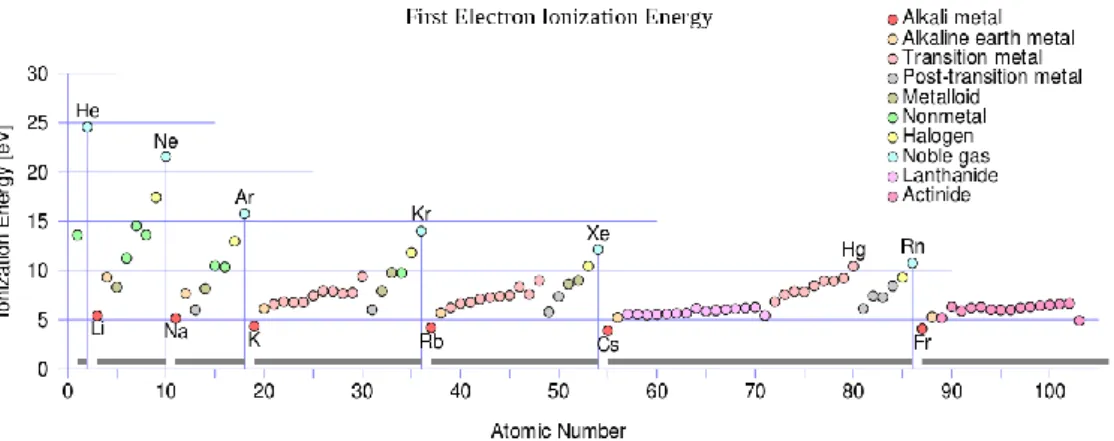
Figure 2-1 : Timestamp of the physical phenomena during ultrafast laser interaction with transparent dielectric materials [9]. --- 7 Figure 2-2 : Schematic representation of Filamentation processes by the intense core of the beam. The solid lines show the diameter of the intense core while the dashed line indicates the root mean square radius of the full beam for linear propagation. The arrowed line in the middle shows the direction of illumination. Modified from [23]. --- 10 Figure 2-3 : Periodic trends for ionization energy (IE) vs. atomic number {copied from
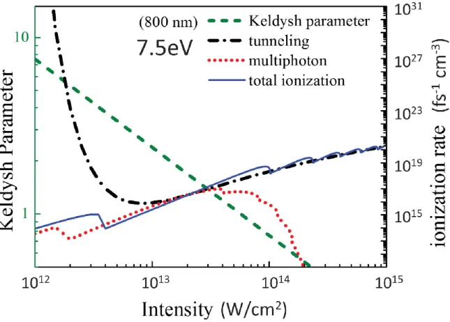
https://en.wikipedia.org/wiki/Ionization_energy} --- 12 Figure 2-4 : Schematic diagram of the photoionization of an electron in an atomic Coulomb potential for different values of the Keldysh parameter. The grey broken line indicates the potential barrier. (Inspired by [22], [25]). --- 14 Figure 2-5 : The photoionization rate and the Keldysh parameter as a function of laser intensity for 800 nm light in fused silica (7.5 eV band-gap). The black dotted line describes tunneling only (equation (40) in [28]); the dotted red line shows multiphoton ionization only (equation (41) in [28]); and the solid blue line is for the full expression from Keldysh (equation (37) in [28]){modified from [22] and [27]}. --- 15 Figure 2-6 : Nonlinear ionization process dominating ultrafast laser writing. (a) and (b) show direct
photoionization processes with multiphoton and tunneling ionization processes, respectively. (c) shows the avalanche ionization process [8]. --- 17 Figure 2-7 : Schematic diagram of two modification regimes in DLW. Athermal and thermal regimes of writing with low and high repetition rate of the pulses, respectively (inspired by [10], [26]). --- 22 Figure 2-8 : Transmission microscope bright-field (BF) images of the damage tracks produced in a Nd:YAG sample by 120-fs pulses at a writing speed of 200 µm/s. The beam was focused from the top. (modified from [16]). --- 24 Figure 2-9 : Refractive index distribution of waveguides written inside LiNbO3 with type I and type II
modification regimes in (a) and (c). The respective beam profiles that are guided along the modified zones are shown in (b) and (d), respectively. The broken line in (b) shows the modified track in (a) and the red ellipses in (d) depict the double damage tracks shown in (c). (modified from [49]) --- 25 Figure 2-10 : Simplified depiction of a crystal. --- 28
them. --- 28 Figure 2-12 : Representation of Bravais Lattices of cubic crystal system. (i) The simple/primitive cubic (sc), (ii) the body centered cubic (bcc) (iii) the face centered cubic (fcc) lattices. --- 29 Figure 2-13 : (a) General three-dimensional representation of second rank tensor, e.g. stress. (b)
Two-dimensional representation of strain with a square that is deformed to a parallelepiped. --- 30 Figure 2-14 : (a) Tensor representation of the form of the elastic compliance tensor for cubic crystallographic systems. Standalone dots represent zeros; dot and a line represent equal components; X represents 2 fold (S11
-S12) approximately while the interconnecting line indicates that they are equal (inspired by [79]) . (b) and (c)
show elasticity, 10-12Pa-1, of CaF
2 and YAG respectively (data from [80]). --- 31
Figure 2-15 : Unit cell of CaF2. The black balls represent the Ca atoms, and the green balls represent the F atoms
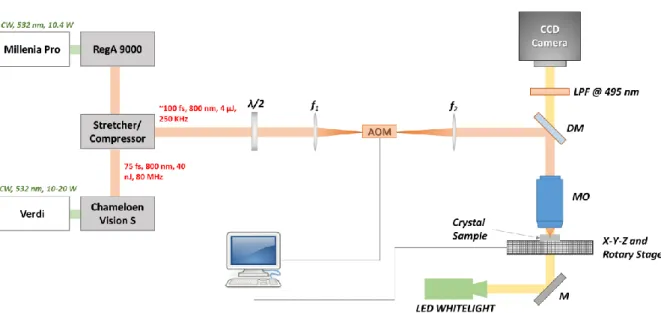
[83]. --- 33 Figure 3-1 : The summary sketch of the 3D direct laser writing setup. λ/2 – half-wave plate; f1 – 1000 mm
convex lens; f2 – 500 mm convex lens; AOM – Acousto Optic Modulator; DM – dichroic mirror; LPF – long pass
filter; MO – microscope objective; M – mirror. The AOM and 3-axis stage are synchronized and computer controlled. An LED white light source and a CCD camera enable in-situ imaging of the sample during
fabrication. --- 39 Figure 3-2 : Relationship between AOM RF Voltage and the fraction of peak power delivered. --- 42 Figure 4-1 : Optical micrograph of femtosecond inscription of matrix of number of pulses/speed of writing (µm/s) and RF voltage (v)/energy of writing(μJ) for undoped CaF2 sample. (a) shows coarse modifications; (b) shows fine tuning around the threshold of modification. The red rectangle shows crack formation while the green rectangle shows the threshold of modification. --- 45 Figure 4-2 : Sketch of two undoped CaF2 samples used for waveguide track fabrication. (a) shows the sample
Group A with polished faces parallel to [112], [110] and [111]. Similarly, (b) shows the sample Group B with polished faces parallel to [043], [134] and [611]. --- 47 Figure 4-3 : Schematic diagram of a conical shaped beam focused at 150 µm mechanical depth below the sample. LEFT: Beam focused inside the sample; RIGHT: beam focused at the edge of the sample. d is the beam diameter at the surface of the sample. --- 50 Figure 4-4 : Microscope images of all the five tracks written inside undoped CaF2 crystal. (a) and (b) are side (xz)
and top (xy) bright field (BF) images in transmission of written tracks with different energies, respectively. (R) - reference single track written to locate the double tracks. (c) shows dark field (DF) image in reflection of a dual track waveguide written with 0.44 µJ. (d) shows the 20X BF image of a transversally sliced part of the sample with thickness, t, of 1.37 mm. --- 51
The polarization is along the y- and x-axis of Sample A in (Case 1, 3) and (Case 2,4), respectively. Furthermore, a and b indicate the scanning directions. --- 52 Figure 4-6 : The fraction of smooth modification for the track inscribed with N ≈ 2000, and F = 12 J/cm2. --- 53
Figure 4-7 : All smoothly modified tracks with non-zero fractions as a function of number of pulses and fluence. (a) and (b) show the two directions of scanning in each axis. --- 53 Figure 4-8 : Plot of all the smooth modifications inside CaF2 and the contour, at 30% of the smooth modification
ratio, shows windows for the writing parameters with respect to the direction of scanning, crystallographic axes, number of pulses per spot and fluence. The gray scale indicates the percentage of the track that is smoothly modified. --- 54 Figure 4-9 : Bright field microscopic image of double tracks. (a) shows section of a smoothly modified track inscribed with case 2 at 240 µm/s (N ≈ 2400) and energy of 0.47 µJ (F = 11.4 J/cm2); (b) shows part of modified
track inscribed with case 2 at 10 µm/s (N ≈ 57000) and energy of 0.67 µJ (F = 16.4 J/cm2) with no smooth
modification. --- 56 Figure 4-10 : Double track written at speed of 240 µm/s (N ≈ 2400) and energy of 0.47 µJ (F = 11.4 J/cm2) with
case 2. (a) shows the two-dimensional refractive index change map of the portion of the double track as viewed from the top; (b) shows the line profile of the refractive index change map. --- 57 Figure 4-11 : Illustration of the differential heating of a crystal as a result of the bulk photothermal effect (copied from [123]). --- 59 Figure 4-12 : Non-reciprocity of writing based on the pixel counts of the written tracks. In the color scale, 0 and 1 show no or smooth modification and the maximum modification in each case, respectively. --- 60 Figure 4-13 : Near field profile images of light guided inside double track waveguides inside CaF2 crystal with
writing directions shown above the sketch of the tracks with circle and x and circle and dot for the inward and outward directions of writing, respectively. (a) HeNe source at 633 nm; (b) and (c) are tracks written by opposite directions of writing with polarizations parallel and perpendicular to the elongation of the tracks, respectively; (d) and (e) are tracks written by same directions of writing with polarizations parallel and
perpendicular to the elongation of the tracks, respectively. --- 61 Figure 5-1 : Schematic plots of the fabrication of the three categories of guiding inside crystal materials by femtosecond laser irradiation and the spatial locations of the waveguide modes: a) waveguides based on Type I modification in single-line geometry, b) waveguides based on Type II modification in dual-line geometry, and c) waveguides based on Type II modification in depressed cladding Type III geometry. [132] --- 66 Figure 5-2 : (a) OPD measurement of double track waveguide, (b) OPD measurement of single track, (c) simple arithmetic addition of two single track OPD measurements and (d) line profiles of the OPD spatial maps of
violet line). --- 67 Figure 5-3 : Refraction and reflection of light at a dielectric interface. The proportion between reflected and refracted beam power can be calculated using Fresnel equations. --- 69 Figure 5-4 : Waveguiding setup. The source @ 633 nm is a HeNe Laser; λ/2_1 and λ/2_2 are half-wave plates; BB1 and BB2 are beam blockers/screens; PBS is a polarization beam splitter; M is a mirror at 45°; OBJ 1 is an Olympus Neo SPlan 5x injecting/focusing objective with NA = 0.13; S is the sample; SH is the sample holder with x-y-z 3D linear translations in addition to rotary translations with polar angle θ and azimuthal angle ϕ; OBJ 2 is an Olympus UPlanFLN 20x imaging with NA = 0.5; P is a pinhole; BP is a Thorlabs BC106N-VIS Charge-Coupled Device (CCD) Beam Profiler. --- 71 Figure 5-5 : Intensity images/ profiles of a micro-scale ruler on the CCD camera position. (a) shows the HeNe laser at 633 nm as a source while (b) shows illumination with white light. I min and I max are the normalized
intensity values at the maximum and minimum radiation intensity; the dark marks are the marks of the micro-scale ruler with 10 µm between them.--- 72 Figure 5-6 : Normalized intensity of measured and smoothed data points for determination of pixel distances between the scales of the micro ruler. (a) blue markers show measured data intensity vertically binned, continuous red lines represent the smoothed data and green discrete line at 35 % of maximum; (b) smoothed data trimmed at 35 % to avoid errors due to background and smoothing.--- 73 Figure 5-7 : PDDs of the injected HeNe laser source and the guided modes of five waveguides. Light blue broken lines show the boundary at 1/e2 of the maximum amplitude. --- 74
Figure 5-8 : Near Field, NF, MFD of modeled power density distributions. (a) Evolved unguided circular Gaussian mode in 2D, (b) Guided elliptical Gaussian mode in 2D, (c) Modeled unguided mode at the exit facet of the sample in 2D and (d) the 3D view of the modeled unguided mode. --- 78 Figure 5-9 : Transmission loss setup. (a) Pout1 is the power output measured as the sum of all the unguided
mode and guided mode collected by focusing optics. (b) Pout2 is the power output measured as the sum of a
portion of the unguided mode and all of the guided. --- 79 Figure 5-10 : (a) The profile of WG-1 with the pinhole edges encircling the guided mode. (b) Binary image of edges and (c) The numerically fitted circle, 2rpin = 64.8 µm, to completely encapsulate the edges. --- 80
Figure 5-11 : Transmission loss (dB/cm) of the CaF2 undoped crystal double-track waveguides in comparison
with some previously reported transmission losses where red is a Nd:CaF2 crystal [75]; black is a Yb:YAG
ceramics [101]; green is a Cr:YAG crystal [109] and blue is a Yb:YAG crystal [106]. The gray line at 0.31 dB/cm is the transmission loss of the CaF2 substrate. --- 83
(a) Normalized transmitted power based on the maximum value of transmitted power as a function of direction of light polarization. (b) Polarization Extinction Ratio (PER) of each waveguide. --- 84 Figure 6-1 : Schematic layout of QWLSI setup for determination of OPD. MHM - Modified Hartmann Mask [150]. --- 88 Figure 6-2: (a) 1D interferogram formation by a MHM in the case of a disturbed input wavefront; geometrical approach. (b) Interferogram obtained with an aberrant wavefront. (c) Zoom on a part of (b), visualization of the local frequency modulations. (d) Fourier Transform of (b). (e) Obtaining of 2 OPD orthogonal gradients by Inverse Fourier Transform of 2 sub-images of (b). (f) 2D Integration of the gradients to reconstruct the OPD and intensity (I) images. The figure is copied and modified from [150]. --- 89 Figure 6-3 : 3D schematic of the double track waveguide inscribed inside the CaF2 crystal. T1 and T2 are the
modified pairs of track; R2 is the region in between the tracks; R1 and R3 are the sidelobe regions of the tracks T1 and T2, respectively; W ≈ 6 µm and H ≈ 40 µm are the average width and height of the tracks, respectively; D = 20 µm is the distance between the tracks T1 and T3; and T = 1.37 mm is the thickness of the sample. --- 91 Figure 6-4 : OPD measurements along the double tracks of the waveguides. (a) and (b) show the OPD
measurement in the lateral (xy-plane), while (c) and (d) show the longitudinal (xz-plane) measurements. (a) and (c) are measurements with the polarization parallel to the track while (b) and (d) show OPD measurements for the polarization perpendicular to the tracks. --- 92 Figure 6-5 : Line profile of the OPD measurements. (a) xy-plane. (b) xz-plane. The solid line shows WG-1; the broken line with one dot shows WG-2; the broken line shows WG-3; the broken line with two dots shows WG-4; and the dotted line shows WG-5. Black color indicates measurements with the polarization parallel to the track, while green color indicates measurements perpendicular to the tracks. --- 93 Figure 6-6 : Near-Field and far field diffraction of a plane wavefront at an aperture slit of diameter 2a. --- 95 Figure 6-7 : (a) Sketch of waveguides with the OPD contributions with discrete elements for different Fresnel zones. (b) The plot of evolution of the OPD contributions from different layers of discrete Fresnel zones with radii b > a. --- 96 Figure 6-8 : 0.5 µm long stairs written with 0.15 µJ at 10 MHz with different distance between them (ds) and
different step in depth (Z). --- 97 Figure 6-9 : OPD (nm) measurement of stairs with an ds of 2 µm and mechanical depth step of 0.1 µm. --- 98
Figure 6-10 : (a) Raw measurement of OPD (nm) of the stairs of Exp # 5 (ds = 3 µm and step of depth = 0.5 µm)
with 0.15 NAcondenser, (b) Normalized, inverted and selected stairs after transformation.--- 100
Figure 6-11 : 2D- and 3D-images of post processing of the selected stairs (Exp#5). (a) Selected and normalized stairs. (b) Fitted stairs to find the smallest element and (c) masked stairs based on the smallest element. (d), (e) and (f) show the respective 3D-images. --- 101
the height of the elliptical cylinder for the same volume of the masked stair; solid blue line – fitted parabolic curve to find the Z intercept, and the red broken line indicates the z intercept at -0.29 µm. --- 102 Figure 6-13 : The OPD contribution of stairs of different experiments with different step and distance between stairs superimposed together. --- 103 Figure 6-14 : Generating a binary mask of double tracks of WG-1. (a) Intensity image of WG-1; (b) Binary mask of double tracks after post processing. The scale bar represents the normalized intensity based on the
maximum intensity values. --- 105 Figure 6-15 : Spatial map of refractive index change (Δn) measurement of WG-3. (a) Spatial map of Δn along the tracks. (b) Spatial map of Δn in the vicinity of the tracks. (c) Spatial map of Δn by blending (a) in to (b). (d) Line profile Δn at the middle of the tracks along the x-axis. --- 106 Figure 6-16 : The three-dimensional spatial Δn of all the five waveguides.--- 107 Figure 6-17 : (a) Line profile of Δn for all the waveguides as it is shown in Figure 6-16 above. (b) The minimum and maximum Δn values of the waveguides. --- 107 Figure 6-18 : Importing the 3D spatial map of waveguides for simulation using Mode Solutions of Lumerical Inc. (a) screenshot of the (n,k) material import wizard; (b) File format for isotropic material and on the left example for WG-1; and (c) Index monitor to view the imported material (in this case for WG-1). --- 109 Figure 6-19 : (a) - (e) show the first five TE modes of WG-1 determined by simulation. (f) shows the plot of overlap between the assumed HeNe source at 633 nm with a radius of 7.5 µm, and the effective refractive index of the five TE modes of WG-1. --- 110 Figure 6-20 : Fundamental power density distribution (PDD) of both simulated (a) and experimental (b) profiles of all the five waveguides. --- 111 Figure 6-21 : Mode-Field diameters of both simulated (squared marks) and measured (circular marks) PDDs.111 Figure 7-1: (a) Image of the cross section and (b) radial refractive index profile of a depressed cladding
waveguide inscribed in sapphire. The profile is computed along the solid blue line, and data are plotted symmetrically on both sides of the central axis. (copied from [155]) --- 115
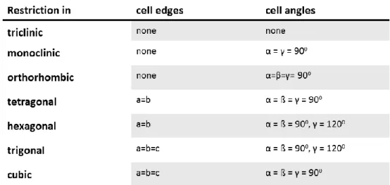
Table 2-1 : The seven crystal systems and the restrictions on their cell dimensions. --- 29 Table 2-2 : Comparison of properties of Yb-doped YAG and CaF2 (copied and modified from [13])--- 34
Table 4-1 : DLW waveguide inscription parameters of CaF2 waveguides. Crack th. – threshold of crack
formation; Mod. th. – Modification Threshold; Ep (µJ) – Energy per pulse; ED (mJ) – Total Energy Delivered at
focal point; F (J/cm2) – fluence; Ev (J/cm3) – Total Energy Deposition per unit volume and I (TW/cm2) –
Irradiance. --- 49 Table 5-1 : Near-Field MFD of double-track waveguides inside CaF2 and the HeNe source. --- 75
Table 5-2 : Transmission loss experiment measured values for three independent experiments. Where DLW E is the writing energy for each waveguide in µJ. --- 82 Table 6-1: Different parameters of the stairs selected for post processing. Exp # - Experiment parameter number; ds – distance between the stairs; Estimated z (µm) – mechanical depth multiplied by the refractive
index of CaF2 at the wavelength of 1030 nm; Measured z (µm) - measured depth under the microscope; P (W) is
the writing power measured just after the AOM in the writing setup; Total # stairs is the number of stairs inscribed for each given parameter. --- 99 Table 6-2 : Calculated Depth of Field for the xz–plane of refractive index measurements. --- 104 Table 6-3 : Simulated results of the effective refractive index (neff) of all the five waveguides for fundamental
modes. The third row shows the effective numerical aperture (NAeff) that should be considered. The last row
1 Introduction
1.1 Motivation and Aim
Light is a form of radiant energy or energy that travels in waves. Throughout the ages, from the Greek philosophers Socrates, Pluto, Euclid to the times of Ibn al-Haytham, who disproved the emission theory of vision from ancient Greek to the recent times of Newton, Huygens, Maxwell and Einstein, many researchers have taken up the challenge to define the nature of Light.
Progress of the study of light over 2000 years leads to the accumulated knowledge which consequently leads to the discovery of the true nature of light, namely photons which are defined as the quanta of light. The photons have many mysterious properties, for example, dual properties of a wave and a particle depending on the type of experiments and interactions with matter. This leads to categorizing light based on its different properties like polarization, wavelength, power, and so on. In accordance with the various properties of light, materials can be made to respond differently for these traits. The property of materials exhibited to light exposure to attain different features distinctly from the non-excited or non-exposed materials, that is relevant to many phenomena and applications, is called photosensitivity. Photosensitivity is essential for applications ranging from photosynthesis and lithography to ultrafast laser writing.
The discovery of lasers, that emit light coherently, gives rise to more effective and diverse applications of light. High power laser applications like laser cutting, drilling, welding and also lithography were possible with lasers thanks to the spatial coherent property which enabled a laser to be focused to a tight spot. Similarly, the temporal coherence property of lasers can be used to generate very short femtosecond pulses as well as single-frequency sources.
The advent of powerful lasers that can produce coherent pulses in the femtosecond regime when mode-locked have opened new frontiers in material research with extremely short temporal and high spatial resolutions. In fact, the breakthrough of the amplification technique called “CPA” (chirped pulse amplification) has been awarded the Nobel prize in 2018. Concurrently, laser-induced damages in transparent materials have been subject of numerous studies over more than the past two decades. Since the 1970s, experimental and theoretical investigations related to damages in silica glasses by the effect of UV radiation, that are equivalent in energy per photon with interband transitions from the valence to the conduction band, have been underway [1]. However, in 1996, following the pioneer work of Hirao’s group on the laser damage inside transparent dielectric materials, there was a breakthrough in femtosecond laser dielectric material processing, materials that do not have any linear absorption at the wavelength of the femtosecond laser, by visible and IR lasers with high-energy-density femtosecond sources [2]. Following this paradigm shift, there have been rapid developments and applications of both surface and volume processing of dielectric materials using ultrafast lasersthanks to the fast growth in wide implementation and advancement of ultrafast lasers for both fundamental research and practical applications during the same period [3]. As a result, dramatic progresses and intensive studies with more modified systematic approaches and techniques of ultrafast laser writing have shifted ultrafast laser writing from scientific curiosity to standard fabrication techniques. For example, recently ultrafast laser written waveguides are becoming comparable with quality to those produced with other more conventional techniques while being less expensive [4].
The generalized model of bulk damage in homogenous dielectric materials by ultrafast lasers involves a combination of nonlinear absorption processes resulting in the excitation and heating of electrons followed by transfer of this heat energy to the surrounding lattice. The deposition
of this energy induces, by a variety of mechanisms, refractive index modifications localized over a micrometer-sized volume of the material. By combining these localized modifications with the 3D movement of the focal volume of the ultrafast laser beam, it is possible to inscribe optical waveguides or more complex photonic circuits.
In comparison with other material modification techniques, e.g. photolithography, there are unique advantages in favor of ultrafast laser micromachining of bulk transparent materials [5] to mention but a few:
• Damages are extremely confined: The nonlinear nature of the absorption confines any induced changes to the focal volume in combination with laser-beam scanning or sample translation making it a simpler and less expensive device production technique for compact photonic systems [6].
• Enables rapid prototyping: The setup usually gives access to simple software control of the writing patterns and parameters. This results in a significant cost reduction of production with respect to standard techniques.
• Intrinsically a three-dimensional (3D) technique: Since the nonlinear absorption process is more or less independent of the type of material and localized to the focal volume, the refractive index changes can be induced at any point inside the bulk material, 10 μm to 10 mm from the surface. This capability can be manipulated to implement fabrication of novel devices, for example an ‘optical motherboard’ [7]–[9].
Consequently, these advantages resulted in a rapid progress of ultrafast laser micromachining which gives rise to realization of vast ranges of photonic devices. This is a driving force behind industrial interest for rapid prototyping of optical components [10]. Among its vast implementations, there have been a growing number of applications for high repetition rate laser systems which can be achieved through functionalization of laser systems and subsystems by miniaturizing photonic components. Highly efficient crystalline waveguide lasers have been demonstrated and can be realized with waveguides inside optically active media [11]. For
instance, waveguides, that can be inscribed using ultrafast laser micromachining techniques, offer a confinement and an excellent overlap between pump and laser modes over the entire length of the medium. Thus, given the very small pump and laser mode diameters, a large gain can be achieved, resulting in laser systems with small laser thresholds. Moreover, resonator mirrors can be achieved by coating end facets of the waveguides, inscribing Bragg structures or with optical contact. The integration of saturable absorbers to the combination of a waveguide and integrated mirrors can result in cost effective, highly efficient, stable and robusthigh repetition rate mode-locked lasers. In general, this is the motivation behind this thesis work.
The entirety of this thesis project is dedicated to crystalline materials due to the superiority in thermomechanical properties and higher emission/absorption cross sections of rare earth doped crystalline materials as compared to glasses. The method to identify parameters of ultrafast laser inscription of waveguides inside crystalline materials has been presented. In parallel, the thesis aspired to refine the approaches for qualitative and quantitative characterizations of the waveguiding properties of modified transparent materials, namely transmission loss of the guided modes and a very accurate determination of the three-dimensional refractive index change of the modified material.
This thesis commenced with the study of double track waveguides inside Neodymium-doped Yttrium Aluminium Garnet (Nd:YAG). As it is a common crystal widely used as gain medium in solid state lasers, several studies had already been done and presented on Nd:YAG [12]. Thus, a study of double track waveguides was performed with the intention to confirm and attest our experimental and theoretical approaches. Furthermore, due to its scalability during crystal growth and competitive spectroscopic, mechanical and thermo-optical advantages specially for diode- pumped large-scale high-energy lasers, CaF2, as “new old laser material”,
is blooming to become a better candidate as a host material[13]. We chose to study both YAG and CaF2, the large part of the project was dedicated to CaF2. Taking into account that both
crystals are cubic, owing to their crystallographic structures, optical specificities and restrictions of low-symmetry crystal optics are neglected which enables a more simplified
systematic approach to study modifications due to ultrafast laser micromachining along the micro-modified zones of the crystals.
In Chapter 2, a brief theory on laser matter interaction during ultrafast laser micromachining, and the properties of crystals of interest is presented followed by the experimental procedures to inscribe waveguides in Chapter 3. In Chapter 4, anomalies during ultrafast laser micromachining which resulted in non-reciprocal, ‘quill’, writing and smooth modification is discussed together with double track waveguide inscription at different pulse energies inside CaF2 crystals. While Chapter 5 is dedicated to briefly summarize a refined quantitative and
qualitative modeling of the approach and result for transmission loss measurements of the guided modes inside double track waveguide in CaF2 crystals. Followed by Chapter 6, which
is also dedicated to characterizing the waveguides using the Fresnel number approach to generate the 3D map of refractive index change measurements implementing the phase-contrast microscopy method. Chapter 7 concludes the main tasks accomplished during the thesis. Finally, the work on Nd:YAG by our group is briefly presented in the Appendix A.
2 Laser-Matter Interaction in Crystals
Despite the promise of femtosecond laser pulses in processing wide bandgap dielectric materials for a variety of applications, understanding the fundamental aspects of intense femtosecond laser interactions with dielectrics has been a challenging task. It is the objective of this chapter to provide the theoretical overview of recent efforts at uncovering the subtleties of femtosecond laser interactions with wide bandgap dielectrics, crystals in particular. In the upcoming Section 2.1, the ultrafast time-resolved studies of the dynamics of electronic excitation and pulse propagation that are related to material modification are discussed. Moreover, types of modifications in crystals and the fundamental aspect of crystals together with the crystals of interest and the state-of –the-art are discussed in Sections 2.2, 2.3, 2.4 and 2.5, respectively.
2.1 Fundamental Principles of Laser-matter Interaction
Due to historical reasons, and in relation to semiconductor light sources used for telecommunications, most lasers, for example Yb/Nd:YAG lasers, many fiber lasers and the most powerful laser diodes, emit near-infrared light. Comparatively, there are fewer laser sources for the mid- and far-infrared spectral regions and also in the UV regime. However, most dielectric materials used for photonics systems and subsystems are transparent to near-IR lasers. Consequently, for the ease of its accessibility, the study of the processes of material response following exposure to intense near-IR femtosecond laser irradiation are far more complex, particularly for wide bandgap dielectrics, which are transparent for photons at this wavelength. However, when a dielectric material is subjected to focused femtosecond laser irradiation with a sufficiently high pulse peak intensity, the absorption of the material becomes intensity dependent, and a large amount of excited electrons are generated as free carriers. This
phenomenon followed by relaxation channels of electronic excitation in wide bandgap materials in relation to heat deposition to the surrounding lattice produces photo induced defects in the otherwise “defect-free” medium [14].
Figure 2-1 : Timestamp of the physical phenomena during ultrafast laser interaction with transparent dielectric materials [9].
The underlying physical phenomena that describe an intense ultrafast laser beam writing inside a dielectric material is accepted as a three-stage process resolved temporally as electronic (carrier) excitation followed by thermalization and localized structural modifications as shown in Figure 2-1. Understanding the timescale of different physical phenomena provides a detailed insight into why femtosecond laser pulses are useful for micromachining applications of dielectric materials. In addition, the nonlinear excitation gives femtosecond laser-induced damage confinement and repeatability. Firstly, the intense laser beam focused into the material, gets absorbed and generates electrons. These electrons then form a plasma and consequently transfer their kinetic energy to the lattice over a picosecond timescale. Within a couple of nanoseconds, a pressure or a shock wave due to subsequent relaxation of stress [9] separates from the focal volume followed by a large density distribution change coupled with accompanying the heat diffusion out of the focal volume at a nanosecond and microsecond scale. For sufficiently high pulse energy, these thermodynamic processes result in material melting and microexplosions, leaving behind permanent structural changes [9], [15].
2.1.1 Nonlinear Propagation and Filamentation
For large pulse powers, provided that the ultrafast laser beam will also undergo nonlinear propagation inside the dielectric material which modifies the spatial intensity distribution that can rather be described with linear terms, the process of laser-matter interaction at high intensities is much more complex [16]. The main nonlinear mechanisms affecting the propagations are:
1. Nonlinear Polarization for self-focusing (Optical Kerr effect): When light propagates inside a transparent dielectric material, it induces oscillating electric dipoles at a microscopic level that give rise to a cumulative macroscopic polarization. The polarization vector could be expanded as a Taylor series whose coefficients are the nonlinear susceptibilities. Thus in dielectric materials which have an inversion center (χ(2) ≈ 0), the polarization vector, P, can be approximated as [17]:
𝑷 ≈ 𝜀0[𝜒(1)+3 4𝜒
(3)|𝑬|2] 𝐸 (2.1)
Where E is the electric field vector; PL = ε
0χ(1)E is the linear part of the polarization;
while PNL = ε
0χ(3)|E|3 represents the nonlinear part of the polarization. Thus, the total
distribution of refractive index can be given as [8]:
𝑛 = √1 + 𝜒(1)+ 𝜒(3)|𝐸|2 ≈ 𝑛
0+ 𝑛2𝐼 (2.2)
Where 𝑛0 = √1 + 𝜒(1) is the linear refractive index, 𝑛
2 = 3𝜒(3)/𝜖0𝑐𝑛02 is the
nonlinear refractive index and I = ε0n0c|E|2/2 is the laser intensity. According to the
expression above, the spatially varying refractive index relative to the intensity of the beam acts as a positive lens, for positive n2 in most dielectric materials, and further
index is exclusively related to the local intensity or simple peak power of the beam. Thus, as the peak power of the laser beam increases, self-focusing of the beam plays a role to overcome the beam diffraction and it might lead to collapse if the input peak power exceeds a critical threshold, Pcr, defined as [18]:
𝑃𝑐𝑟 = 3.72𝜆
2
8𝜋𝑛𝑛2 (2.3)
Where λ is the wavelength of the source; n and n2 are the linear and nonlinear refractive
indices, respectively. The origin of such a critical power is the dependence of the refractive index of the material on its polarizability in which this critical point is also the indication of saturation of the effective polarizability, i.e. the point where all molecules are aligned with their “easy” axes of polarizability [18]. For example, this critical point is calculated for both CaF2 and YAG as 5.3 MW and 0.8 MW,
respectively.
2. Plasma defocusing: In reality, the self-focusing of the beam is usually sufficient enough for an abrupt onset of multiphoton absorption instantaneously followed by electron plasma formation. The free electrons inside the plasma will then contribute to a negative refractive index gradient which can be approximately expressed as [19]:
𝑛𝑃 = 𝑛 −
𝑁(𝑟, 𝑡) 2𝑁𝑐
(2.4)
Where nP is plasma refractive index; n is the refractive index of the bulk material; N(r,t)
is the density of free electrons, . The critical density of carriers, Nc, can be given as [20]:
𝑁𝑐 =(4𝜋2𝜀0𝑚𝑒𝑐2)
(𝑒2𝜆2)
Where ε0 is the permittivity of free space; me is the mass of electron; e is the charge of
the electron; c is speed of light; and λ is the wavelength of the laser source. For example, for the laser at 1 µm wavelength, this point is achieved for the carrier density of 1021 cm-3. Thus, this defocusing effect of the plasma counter acts the positive refractive index change produced by the Kerr effect, resulting in a defocusing of the beam. The interplay between these two nonlinear effects will lead to the propagation of the beam at a very small size over several Rayleigh distances and the process is called Filamentation [8], [21], [22].
Figure 2-2 : Schematic representation of Filamentation processes by the intense core of the beam. The solid lines show the diameter of the intense core while the dashed line indicates the root mean square radius of the full beam for linear propagation. The arrowed line in the middle shows the direction of illumination. Modified from [23].
As it is depicted in Figure 2-2, the combination of the optical Kerr effect, multiphoton absorption, MPA, and ionization result in the origin of the formation of the first cycle of the filaments preserving an average small diameter over a long distance. This beam at this cycle is further attenuated by mainly losses due to plasma absorption and multiphoton ionization. As the pulse further propagates, it is nonlinearly refocused and becomes sufficiently intense with a peak power above Pcr which should undergo a collapse. However, MPA attenuates the core
of the beam and a plasma is generated once more near the collapse location, which defocuses the beam core once again and gets attenuated because of nonlinear losses as described above.
The repetition of this scenario sustains a long range, self-guided propagation in the form of a filament [23].
2.1.2 Nonlinear Photon Absorption and Propagation
The phenomenon of carrier excitation by direct absorption of photons is generally called photoionization. In the simplest case, the laser linearly deposits energy into a material by creating an electron-hole plasma through single-photon absorption. However, the absorption cross section is very small at IR wavelength for wide bandgap dielectrics. Consequently, the only way such materials can absorb a sufficient amount of photons from an IR laser is through nonlinear processes which occur at very high intensities commonly described as strong electric field ionization (SEFI).
This can be explained by a simple consideration of a free electron of charge, e-, interacting with linearly polarized light E exp(-iωt),where the position x of e- under this harmonic motion can be given as:
𝑥 = −𝑒𝐸 exp (−𝑖𝜔𝑡)
𝑚𝑒𝜔2
(2.6)
Where e is the charge of an electron; me is the mass of an electron; ω = c / λ is the frequency
of the laser source. Given the cycle-averaged intensity as I = cεE2/2 where c is the speed of light, ε is the permittivity of the dielectric material and E is the electric field amplitude.
Therefore, the cycled-averaged kinetic energy, Ponderomotive energy, Up, the electron
𝑈𝑝 = 1 2𝑚𝑒𝜔 2〈𝑥2〉 = 𝑒 2 8𝜋2𝑚 𝑒𝜀𝑜𝑐3 𝐼𝜆2 (2.7) 𝑈𝑝[𝑒𝑉] = 9.34 × 10⁻²⁰× (𝜆[𝑛𝑚])2 × 𝐼 [𝑊 𝑐𝑚⁄ 2] (2.8)
Where λ[nm] is the wavelength of the source in nm; ε0 is the free space/vacuum permittivity.
The nonlinear ionization process via SEFI occurs when the absorbed Ponderomotive energy is greater than the ionization potential or the bandgap energy of the system, Eg, Up > Eg. For
example, as shown in Figure 2-3, the ionization energy of most elements falls between 5 – 20 eV which corresponds to the intensity of 5 - 20 x 1013 W/cm2 approximately for a source at 1030 nm [25].
Figure 2-3 : Periodic trends for ionization energy (IE) vs. atomic number {copied from https://en.wikipedia.org/wiki/Ionization_energy}
Experimentally, it has been proven that, for the nonlinear multiphoton absorption inside a dielectric material of ultrafast laser radiation to occur, the peak intensity of the IR laser beam should be at least in the regime of 1012 to 1013 W/cm2. At these intensity values, simultaneous
absorption of multiple photons is involved to excite a valence band electron. This type of photoionization by direct absorption of multiple photons is called multiphoton absorption. The rate of multiphoton absorption is expressed as:
{𝑑𝑁 𝑑𝑡}𝑀𝑃𝐴
= 𝜎𝑚𝐼𝑚 (2.9)
Where N is the density of electrons in the conduction band; I is the laser intensity and σm is the
absorption cross-section related to m-photons process [7].
The number of photons, m, should be the minimum integer that satisfies the relation, mħω > Eg, where ħω is the single-photon energy; Eg is the bandgap energy of the dielectric material.
Since the multiphoton absorption process is related to the peak intensity of the ultrafast laser beam, it is confined to the focal volume of the laser beam. It provides the initial seed electrons that are heated up by inverse bremsstrahlung forming a high-density electron gas in the conduction band through avalanche ionization processes [26].
Similarly, if the electric field strength becomes comparable with the atomic Coulomb potential, the electron can tunnel through the potential barrier. In this case, the tunneling time is given by the mean free time of an electron passing through a barrier of width, ltunneling = Eg/eE(t, ϕ),
where Eg is the ionization potential, e is the electron charge, and E(t, ϕ) is the optical field. Due
to this inverse relationship between a barrier width and the applied optical field strength, for very high electric fields of the laser pulse, the Coulomb well is suppressed enough that the electron can tunnel through the short barrier and become excited to the conduction band. This type of photoionization is called tunneling ionization [27].
At high intensities of electromagnetic fields, the multiphoton and tunneling ionization processes compete. This behavior of an atom is commonly analyzed based on the Keldysh parameter which is given as:
𝛾 = 𝜔
𝑒√
𝑚𝑒𝑐𝑛𝜖𝑜𝐸𝑔
Where ω is the laser frequency; I is the laser intensity at the focus; Eg is the ionization potential
or bandgap energy of the material; me is the effective electron mass, e is the fundamental
electron charge, c is the speed of light, n is the linear refractive index and ε0 is the permittivity
of free space [28].
The Keldysh parameter can be introduced to define the transition between the regimes of photoionization. For high frequency and moderate intensity of the laser, γ >1.5, multiphoton ionization dominates. Contrarily, for very high intensity ( >1014 W/cm2 ) and lower frequencies,
γ < 1.5, the laser radiation significantly modifies the Coulomb potential, i.e. tunneling ionization dominates the overall initial process of photoionization.
Figure 2-4 : Schematic diagram of the photoionization of an electron in an atomic Coulomb potential for different values of the Keldysh parameter. The grey broken line indicates the potential barrier. (Inspired by [22], [25]).
Figure 2-4 represents the schematic of the three regimes of photoionization described above. In the intermediate regime, i.e. γ ~ 1.5, the overall process of photoionization is a mix between multiphoton absorption and tunneling ionization. For instance, for our case with a laser source at 800 nm, for the given laser beam focusing conditions and material properties, the waveguide fabrication in both CaF2 and Nd:YAG samples results γ < 1.5, i.e. 1.13 and 0.39 for CaF2 and
Nd:YAG respectively, in which the nonlinear ionization is interplay of both multiphoton ionization and tunneling ionization dominated by tunneling ionization specially for the Nd:YAG case [8].
Figure 2-5 : The photoionization rate and the Keldysh parameter as a function of laser intensity for 800 nm light in fused silica (7.5 eV band-gap). The black dotted line describes tunneling only (equation (40) in [28]); the dotted red line shows multiphoton ionization only (equation (41) in [28]); and the solid blue line is for the full expression from Keldysh (equation (37) in
[28]){modified from [22] and [27]}.
In general, the Keldysh parameter provides a common framework for different photoionization processes which would have rather been described with totally different conceptual depictions and analytical formulations [22]. As it can be shown in the
Figure 2-5 above, the solid (blue) line represents the photoionization rate based on the full expression from Keldysh (equation (37) in [28]), the dotted (red) line represents the multiphoton ionization rate, the dashed and dotted (black) line represents the tunneling ionization rate and the dashed line represents the Keldysh parameter. Note that the multiphoton and tunneling rates overlap around a Keldysh parameter of 1.5.
![Figure 2-1 : Timestamp of the physical phenomena during ultrafast laser interaction with transparent dielectric materials [9]](https://thumb-eu.123doks.com/thumbv2/123doknet/12709506.355974/37.892.126.783.291.607/timestamp-physical-phenomena-ultrafast-interaction-transparent-dielectric-materials.webp)