Development of Intersubband Terahertz Lasers
Using Multiple Quantum Well Structures
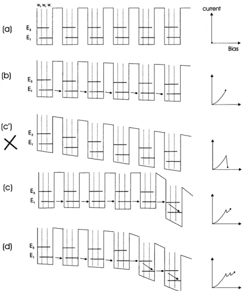
by
Bin Xu
Submitted to the Department of Electrical Engineering and Computer
Science
in partial fulfillment of the requirements for the degree of
Doctor of Philosophy
at the
MASSACHUSETTS INSTITUTE OF TECHNOLOGY
September 1998
©
Massachusetts Institute of Technology 1998. All rights reserved.
A uthor
...
...
.
...-...
..
....
....
Department of Electrical Engineering and Computer Science
August 26, 1998
Certified by...
S...
...
...
.
Qing Hu
Associate Professor of Electrical Engineering and Computer Science
Thesis Supervisor
Accepted by ...
...
Arthur C. Smith
Chairman, Departmental Committee on Graduate Students
MASSACHUSETTS INSTITUTE OF TECHNOLOGY
NOV 16 1998
LIBRARIES
Development of Intersubband Terahertz Lasers Using
Multiple Quantum Well Structures
by
Bin Xu
Submitted to the Department of Electrical Engineering and Computer Science on August 26, 1998, in partial fulfillment of the
requirements for the degree of Doctor of Philosophy
Abstract
This thesis describes an experimental and theoretical effort in developing intersub-band THz lasers using multiple-quantum-well structures. Scarcity of compact solid state sources in this frequency range, and to demonstrate a novel unipolar laser tech-nology, motivated this research. Transport studies for realizing THz intersubband population inversion, new methods for long-wavelength mode confinement, and far-infrared spectral measurement techniques are critical steps in achieving this goal.
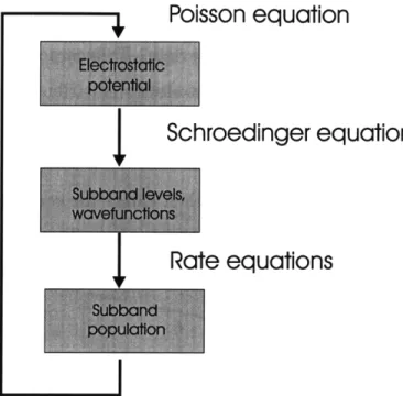
Conduction-band three-level subband systems in triple-quantum-well structures using GaAs/Alo.3Gao.7As heterostructures were proposed, designed, and simulated by
a numerical method. The numerical simulation is a self-consistent solution among the Schr6dinger equation, Poisson equation, and rate equations. Electrons are injected by resonant tunneling to populate the upper subband; the lower subband is depopulated by fast longitudinal optical (LO) phonon scattering. THz emission devices consist of many modules of such triple-quantum-structures with the three-level systems cascade connected to each other. Dynamic charge of electron is provided by the 6-doping per module. Temperature-dependent intersubband scattering plays a key role in transport modeling and therefore the degree of population inversion. Systematic calculations were performed to address issues of hot electron effect, lattice heating, and non-equilibrium optical phonons. Guidelines for device design and optimization were provided. The measured dc I-V at cryogenic temperature confirmed the design expectations.
Plasma confinement is used for making THz laser cavities. The minimum cavity loss can only be achieved by using metallic waveguides. The first metallic waveguide, which incorporates non-alloyed ohmic contact, was successfully fabricated by com-bining wafer bonding and selective etching techniques. Schemes for THz emission couplings were investigated by quantifying coupling loss, including surface coupling by gratings and edging coupling by facets.
The first free-space THz spectral measurement system was developed using a Fourier Transform Infrared (FTIR) spectrometer. This experimental set-up was suc-cessfully demonstrated in resolving THz emission by using step-scan and lock-in tech-I~__~_ _I _____
niques, and a fast Ge:Ga photon detector. Spontaneous intersubband THz emission was observed with linewidth narrower than 0.65 THz, and center frequency at the designed value of 3.8 THz. Different triple-quantum-well structures were designed, grown, and tested. The measured emission power levels were one order of magnitude lower than calculated values, and possible extra cavity loss mechanisms were dis-cussed. To verify the triple-quantum-well structure design, a mid-infrared absorption measurement was performed on a sample grown on semi-insulating substrate. Infor-mation such as subband energy separations, dipole moments, and linewidth broad-ening, was extracted from the absorption spectrum and gave a good confirmation on numerical simulations and MBE growth quality of the MQW structures.
Thesis Supervisor: Qing Hu
Acknowledgments
My these several years of staying at MIT have been an enjoyable and rewarding period. I own a great deal of gratitude to many people that made it possible. Foremost, I want to thank my thesis advisor, Professor Qing Hu, for providing me this challenging research project. His insight, support, and patience have guided me through the difficult periods. I thank him for seeing me through. My thanks go to Professor Terry P. Orlando and Professor Steve Senturia, for not only showing their interest in my research work, but also assigning me a TA duty. I should have accomplished it with much better outcome. I like to thank Professor Clifton Fonstad and Professor Erich Ippen, for acting as my thesis readers. I also want to mention Professor Jesuis del Alamo, for providing me extra guidance through my area examination.
I have been lucky staying in an intelligent research group. It provides me a stimulating environment, which I consider as one of the best pieces of experience in graduate school education. I was impressed by Jurgen H. Smet, whose talent and dedication gave me the very first incentive. I also want to thank him for showing me with hands-on wafer processings. Rolf A. Wyss, Dr. Simon Verghese, and Dr. Gert del Lange are experimentalists, whose skills gave me a sense of how to enjoy lab work and never get frustrated. I want to thank my groupmates: Ilya Lyubomirsky, Ben Williams, Yanko Sheiretov, Brian Riely, Noah Zamdmer, Erik Duerr, Arifur Rahman, and Kostas Konistis for their special skills, dedications, and enjoyable companion. I like to thank Ben Williams for his reading of my thesis draft and corrections of my poor English. I had numerous night-time discussions with Farhan Rana when heading back to Ashdown, with topics ranging from physics to religions.
My sincere thanks go to Professor Mike R. Melloch at Purdue University. He is responsible for wafer's MBE growth. Without his collaboration and prompt run each time upon request, this research project would be impossible.
During my initial period of starting this project, I received a number of helps on device fabrications and clean room facility training from Jim Erystermeyer, David
Contents
1 Introduction 25
1.1 Intersubband transitions for infrared generations . ... 25
1.1.1 Mid-infrared quantum cascade lasers . ... 26
1.1.2 Mid-infrared superlattice lasers . ... 30
1.1.3 Other methods for infrared generations based on intersubband transitions . . . 34
1.2 Existing coherent terahertz sources and applications ... . 38
1.3 Electrically-pumped intersubband THz lasers . ... . . . 40
1.4 Thesis outline ... ... .. ... 43
2 Multiple Quantum Well Structure Design 45 2.1 Introduction . .... .. . . . .. . . . .. ... . 45 2.2 Numerical simulation ... 46 2.2.1 Device modeling ... 46 2.2.2 Simulation code ... ... .. 49 2.3 Triple-quantum-well design: M10 . ... . 50 2.4 High-field domain ... ... ... . . 61 2.5 I-V curves of M10 at 4.2 K ... ... .. 63 2.6 Sum m ary . . ... . . . .. ... ... ... . 74
Introduction ... ... .... Spontaneous emission and gain . . . ... Photon rate equation and sub-threshold spectrum Grating coupling for intersubband emission . . . .
THz mode confinement and cavity loss . . . . Conclusion . . . .. . . . .
4 Temperature Effects on Intersubband Scattering
4.1 Introduction .. .. . . . . 4.2 Intersubband phonon scattering . . . . 4.2.1 LO-phonon scattering and hot electron effect . . . . . 4.2.2 Acoustic phonon scattering and lattice heating . . . 4.3 Non-equilibrium LO phonons . . . .
4.3.1 Intersubband LO-phonon emission and absorption . . 4.3.2 Non-equilibrium LO-phonon population . . . . 4.3.3 Modified subband populations . . . . 4.3.4 Numerical modeling of electron transport . . . . 4.4 Discussions .. ... . . . .. .
5 Measurement Setup and Device Fabrications
5.1 Introduction ... .. . .. .... .... . .... 5.2 THz spectral measurements ...
5.2.1 Measurement set-up . . . . 5.2.2 Emission measurement issues . . . .
5.2.3 Optical power collection efficiency . . . . 5.3 Device fabrications ...
5.3.1 Device processing for spontaneous emission . . . . 5.3.2 Metallic waveguide fabrication for THz laser devices .
109 109 110 112 119 125 126 128 136 139 140 143 . .... 143 ... 144 . . . . . 144 . . . . . 151 . . . . . 155 .. .. . 156 . . . . . 156 . . . . . 158 3.1 3.2 3.3 3.4 3.5 3.6 . 108
6 THz Intersubband Emission
6.1 Introduction . . . . 6.2 Mid-infrared absorption measurement . . . . 6.3 THz emission results ...
6.3.1 Blackbody radiation vs. intersubband emission . . . . . 6.3.2 THz emission from M100 structure . . . . 6.3.3 THz emission from A10 structure . . . . 6.3.4 THz emission from metallic waveguide LSN80 structure 6.4 D iscussions . . . .
7 Conclusions
A Grating coupling for detection B Device processing
C MBE-growth sheets of MQW structures
169 .... 169 ... . 170 ... . 175 . . . . 175 S. ... 182 ... . 188 ... . 194 .... 198 201 209 213 217
List of Figures
1-1 (a) Two-level mid-infrared quantum cascade laser based on local k-space population inversion. Electrons leak out E2 subband at a slower rate than the intersubband scattering rate from E3 to E2 by LO-phonon scattering, resulting in more electrons on E2 subband than E3 sub-band. Optical gain only depends on local k-space population inversion in the vicinity of kll = 0, due to band nonparabolicity, as indicated by the dashed circle region. Electrons scattered to E2 subband from E3 subband loss energy by sequential intrasubband LO-phonon scat-tering. The graded shadow indicates electron occupation in kll space. (b) Three-level quantum cascade laser with global subband population inversion. Optical gain depends on the local k-space population in-version as the case in (a), but the degree of population inin-version is enhanced by reducing the total population on E2 level. ... . 29
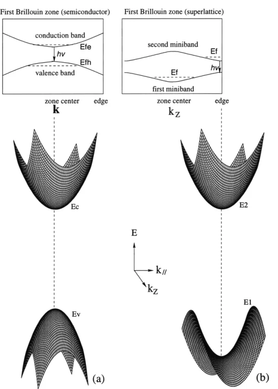
1-2 (a) Valence band and conduction band dispersion relations for a direct band gap semiconductor material in the first Brillouin zone. Under injection condition, Efe is the electron quasi Fermi level in conduction band and Efh is the hole quasi Fermi level in valence band. Lasing transition occurs at the Brillouin zone center. (b) Dispersion relations of the first and second minibands of a mid-infrared superlattice laser, E, = E1 (kz, k1) and E2 = E2(kz, k1l), in the first Brillouin zone. The lasing transition occurs at the Brillouin zone edge, where energy sepa-ration is minimum. Quasi Fermi level is assumed for each miniband.. 31 1-3 Design options for THz intersubband lasers. (a) Scheme-1, three-level
system designed for global intersubband population inversion. (b) Scheme-2, local kz-space population inversion with a superlattice struc-ture. (c) Scheme-3, local kil-space population inversion in valence band, due to non-monotonic light hole subband dispersion relation. ... 42
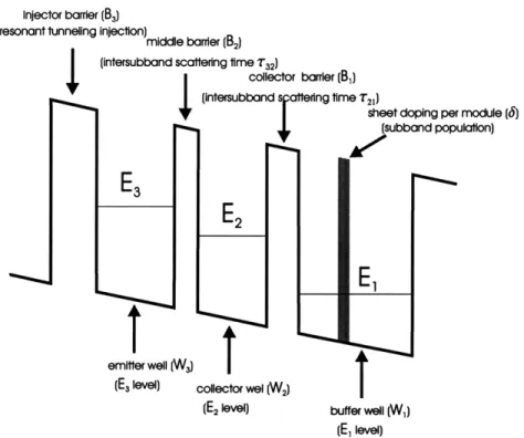
2-1 Device modeling for numerical simulations of the MQW structures . . 49 2-2 Design parameters of a triple-quantum-well structure and their primary
functionality. ... . ... 51
2-3 Transmission coefficient of a single triple-quantum-well module of M10
structure at zero bias. ... 54
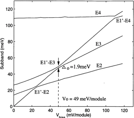
2-4 Simulated subband energy levels as functions of bias per module for M10 structure. E1 level is the zero energy reference. . ... 55 2-5 (a) Self-consistent simulation of M10O structure at required bias, where
E' is aligned with E3. (b) The corresponding charge distribution in the self-consistent solution. The positive charge is due to the sheet donors by 6-doping in the buffer wells. . ... 56 2-6 Magnitude-square of the wavefunctions E' and E3 at resonance
tun-neling vs. the energy separation between E' and E3 . . . . . 58
13
2-7 Subband level separations of M10 structure using self-consistent
simu-lation, as functions of intersubband scattering time ratio, 721 / 3 2. . . 60 2-8 High-field domain development in multiple-module MQW structures
used for THz emissions. ... 62
2-9 Electron concentration (per cm3) at the contact/MQWs junction for M10 device, simulated by a classic Poisson solver at temperature of T=40 K. Two doping levels are used in the contact, 2 x 10¹⁷/cm 3 and 8 x 10¹⁷/cm3 . .... . . . . . 65 2-10 (a) Measured M10 device dc I-V curve at 4.2 K, with loop sweep voltage
between 0 V and 2.7 V. The current density at designed operation bias Vo = 0.49 V is Jo = 0.39 KA/cm2. (b) Simulated M10 subband levels
at bias of 110 mV/module. ... 66
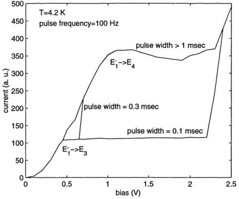
2-11 Measured pulsed I-V curves of M10 device with different pulse widths. The pulse frequency is the same for the three curves. . ... 68 2-12 Measured dc I-V curve of M100 device. The current density at designed
bias V = 4.9 V is Jo= 0.68 KA/cm2 . . . . 70 2-13 Measured dc I-V curves of M10p and M10pp devices. The current
densities at designed bias of V = 0.49 V is Jo = 1.3 KA/cm2 for M1Op
and Jo= 3.6 KA/cm2 for MlOpp. ... 71
2-14 (a) Simulated subband levels under reverse bias of V = -0.15 V/module. (b) Measured reverse biased dc I-V curve of M10 device. . ... 73
3-1 Calculated intersubband spontaneous emission times in 3D case (a) and 2D case (b) as functions of the emission frequency, with different
dipole moment (A)... 81
3-2 Calculated peak gain as a function of emission frequency with different dipole moment (A). The intersubband population inversion is 3 x 10¹⁰/cm2 and the length of one module is im = 300
A
... 833-3 Wave intensity (Mega-Watt per centimeter square) in cavity and THz laser power output as functions of dipole moment with different linewidth.
Saturation stimulated emission lifetime is taken as 7S-t" = 2 ps. The edge emitting facet area is assumed to be Sf = 20 pm x 3 pm, and air/semiconductor interface reflection coefficient is r = 0.55. ... 85 3-4 A schematic showing in optical cavity, photon created by spontaneous
emission and stimulated emission, and annihilated by stimulated ab-sorption and cavity loss including emission escape. . ... 87 3-5 (a) Ratio of device emission power to the spontaneous emission power,
as a function of peak gain with different cavity loss. (b) Emission spectrum showing emission linewidth with different peak gain. The
arrow indicates the original linewidth corresponding to zero peak gain. 89 3-6 Schematic of a grating coupling for intersubband surface emission. 2a
is the width of the metal stripe and p is the grating period. t is the thickness of the confined MQW layer. f = 2a/p is the metallic filling factor . . . . .. . . . . . . . 91 3-7 Emission coupling efficiency and cavity loss of the grating coupling,
including all orders of the diffracted waves, with three different filling factors. no = 1 for air and n' = 3.4 for semiconductor (GaAs). The frequency of the light is 5 THz, and t = 3 pm. The second y axis shows the grating coupling loss, ag = ,/t. ... . . . . . 94
3-8 2D-layer-thickness-induced resonances in a grating coupling of emission with three different filling factors. Coupling efficiency and coupling loss drop to zero when the layer thickness matches the wavelength of the diffracted waves. In this example, p/As = 0.8. The frequency of the light is 5 T Hz .. . . . . .. . . . .. . 96
3-9 Phonon absorption loss ah (cm-1) of GaAs at T=300 K in THz fre-quency range. Data is plotted using aph = kw/co, where the extinction coefficient k (,. = (n + ik)2) is taken from Ref. [109]. . ... 99
3-10 Drude model calculated free carrier loss for GaAs in THz frequency range at different carrier concentrations, with plasma frequencies indi-cated. Scattering time at different carrier concentrations and temper-atures are extracted from drift mobility measurements [110]. ... 100 3-11 Waveguide structures for plasma confinement and metallic
confine-ment. The gray layers are heavily doped GaAs contacts sandwiching MQW active region. The shallow gray is n-type GaAs substrate. The black layers are metals... ... ... .. 101 3-12 Calculated quasi-TEM mode pattern of the plasma waveguide. Solid
and dashed lines are the real and imaginary parts of the fields. The origin point z = 0 is the middle of the active region. The E field is nor-malized by the impedance of GaAs, 109 Q2. The carrier concentration and scattering time in plasma region are indicated. Plasma cavity loss, confinement factor F, and loss due each layer are given at frequency of 4 THz. The active region thickness is 3 pm. The top and bottom heavily doped plasma regions are 0.1 pm and 4 pm thick respectively. 102 3-13 Plasma cavity loss as a function of photon frequency at different carrier
concentrations in the plasma region. The scattering time at each car-rier concentration is extracted from the room-temperature GaAs drift
mobility measurements ... 103
3-14 Calculated mode pattern of the metallic (Au) waveguide. The carrier concentration and scattering time in plasma region are indicated. The thickness of the plasma layers is 0.1 pm. Cavity loss, confinement factor, and loss due to each layer are given at frequency of 4 THz in comparison with the plasma waveguide. . ... 104
3-15 Metallic (Au) waveguide loss as a function of frequency at different carrier concentrations in the plasma layers. ... . . 105 3-16 Calculated mode pattern of a metallic waveguide showing surface plasma
mode. The carrier concentration and its plasma frequency are indi-cated. Surface plasma mode is characterized by a large buried Ez field
in the thin plasma layers ... 106
4-1 For M10 structure, E3 - E2=15.3 meV, E2 - E1=34 meV, the calcu-lated LO-phonon scattering time for an electron from E3 to E2 (a) and
from E2 to El (b) as a function of its initial in-plane k vector (kinetic
energy) ... 114
4-2 Intersubband scattering times 73L ,em and 72LO em as functions of
elec-tron temperature for M10 structure, showing hot electron effect. In calculations subbands E3 (El) and E2 are assumed to have the same
electrons temperature. ... 116
4-3 For M10 structure, intersubband scattering time 732L em as functions of subband energy separation AE3 2 at two electron temperatures T3 =
Te2 = 100 K and 200. K ... 118
4-4 For M10 structure, (a) acoustic phonon scattering time between sub-bands E3 and E2 as a function of lattice temperature T, including
deformation and piezoelectric scattering. (b) Energy loss per scatter-ing event for deformation and piezoelectric scatterscatter-ing. Te3 = Te2 = 100 K, and n3 = 2n2 = 6 x 10¹⁰/cm 2 . . . . 121
4-5 (a) Calculated form factor IA32 12(q) in phonon scattering using M10
structure as an example. (b) Schematics showing for both acoustic-phonon scattering and LO-acoustic-phonon scattering, only the acoustic-phonons in the vicinity of F point can participate the intersubband transitions. . . . 123
4-6 Schematics showing the origin of hot electron effect in THz intersub-band transitions, using three-level system as an example. Electrons can only be scattered to the lower subband by elastic or quasi-elastic in-tersubband scattering, with subband energy spacing in THz frequency
range ... ... 124
4-7 Decay time of non-equilibrium LO phonons into acoustic phonons in GaAs as a function of lattice (acoustic phonon) temperature T. The solid circles are measured values by Raman spectroscopy taken from Refs. [148] and [153] . ... .. .. . .. ... 130 4-8 (a) LO-phonon mode population due to E2 --+ E1 LO-phonon emission
process in the three-level system in M10 structure. (b) The LO-phonon mode temperature Tph corresponding to (a), showing hot LO-phonon effect due to finite decay time of the optical phonons. . ... . 131 4-9 (a) LO-phonon mode population due to E3 -+ E2 LO-phonon emission
process by hot electron effect on E3 level in M10 structure. (b) Total LO-phonon mode population due to both E2 -+ E1 and E3 -+ E2
LO-phonon emissions. ... 132
4-10 Using non-equilibrium LO-phonon mode population in Figure 4-9(b), (a) reduced LO-phonon population due to E1 -+ E2 stimulated absorp-tion process in M10 structure; (b) reduced LO-phonon populaabsorp-tion due to E2 -+ E3 and E3 -+ E2 stimulated LO-phonon absorption process. 133 4-11 For M10 structure, the non-equilibrium LO-phonon population
ob-tained by the self-consistent solution among LO-phonon generation rate through intersubband emission, LO-phonon annihilation rate through intersubband absorption, and LO-phonon decay rate into acoustic phonons. The subband electron populations and temperatures are indicated. The decay time of LO-phonons into acoustic phonons is 7 ps for a
4-12 For M10 structure, (a) intersubband scattering times as functions of the non-equilibrium LO-phonon population which is indicated by the peak phonon population. The phonon distribution in qjl space is assumed to be the same as in Figure 4-11. (b) Corresponding subband population and population inversion as functions of LO-phonon population. . . 137 4-13 Absolute subband population inversion as a function of total free
car-riers per module for M10 structure. Non-equilibrium LO-phonon pop-ulation is assumed to be proportional to the total free carriers in the structure. . . . . 138 4-14 Modeling of intersubband scattering of M10 structure incorporating
phonon systems. Self-consistent solutions need to be achieved among subband populations, intersubband scattering, and non-equilibrium LO phonons using numerical iterations. . ... 140
5-1 Measurement set-up for revolving THz emission spectrum ... 145 5-2 Emission device mounting, (a) grating-coupled surface emission, (b)
facet-coupled edge emission . ... . . .. . . . . . 147 5-3 Transmissivities of the THz window materials. (a) 0.1 mm
polypropy-lene measured by FTIR. (b) 2 mm high-density polyethypolypropy-lene measured by FTIR. (c) 1 mm sapphire with antireflection coating (solid line) and without (dashed line), provided by Infrared Laboratory. . ... 148 5-4 Relative response of the Ge:Ga photon detector. . ... 150 5-5 Water vapor absorption lines, by measuring the transmission of a 300
K blackbody radiation through air using FTIR and Si-bolometer. The resolution is 0.015 THz. The dashed line indicates the roll-off of the
blackbody radiation power ... 152
5-6 Absolute blackbody radiation power of GaAs in specified frequency range as a function of device temperature. ... . . . . 153
5-7 Schematic showing three-mask processing sequence of THz emission devices. (a) MBE-grown MQW wafer. (b) Device mesa formed by wet chemical etching or RIE. (c) Side wall and bonding path covered with SiO2 or Si3N4 for insulation. (d) Grating definition for surfacing
emission. (d') Edge emission device with top covered by metal. . . . 157 5-8 Photo of the processed wafer, showing grating-coupled surface emission
devices with different periods and bar devices with different widths. 158 5-9 Major steps in metallic waveguide fabrication. (1) Au-Au wafer
bond-ing by thermal compression method. (2) Substrate removal by firstly polishing and then selective etching of the GaAs substrate. The etchant stops at a Alo0.5Gao.sAs etching stopper which is initially grown by MBE
on GaAs substrate. (3) The etching stopper is selectively removed by a different etchant with the MQW structure next to it remains unattacked. (4) Processed metallic waveguide bar device with alloyed
metal layer on the top ... ... 159
5-10 The making of non-alloyed ohmic contact. (a) MBE-grown layers of a thin heavily doped n+ + GaAs region, capped by non-doped LTG
GaAs. (b) Schematic band diagram showing electron tunneling from n+ + region to mid-gap states in the LTG cap layer. . ... 160 5-11 Schematic description of GaAs substrate removal by polishing and
se-lective etching. ... 163
5-12 SEM micrographs of fabricated metallic waveguide devices. The view-ing angle is 450 with respect to the [1 1 0] cleavage facet of the MQWs thin film where the THz radiation is coming out.. ... 164 5-13 Measured two typical dc-IV curves at 4.2 K of LSN80 MQW
struc-ture processed into metallic waveguide devices. The device areas are 100 pm x 100 pm. The designed bias is 4 V. . ... 167
6-1 Wedge waveguide used for absorption measurement. t is the MQW region thickness, w is the semi-insulating substrate thickness. 0 is the angle between the E field polarization and quantum well planes. . . 171 6-2 Mid-infrared intersubband absorption spectrum of LSN80 structure on
semi-insulating substrate at room temperature, obtained by transmis-sion measurements using FTIR linear scan. The dashed line indicates the least-square Lorentzian fit of the two peaks. . ... 172 6-3 Numerically simulated energy levels and square magnitude
wavefunc-tions of the subbands in LSN80 triple-quantum-well structure at zero bias. The arrows indicate intersubband absorptions at mid-infrared. The simulation does not include nonparabolicity. The height of the
Al0.3Gao.7As barrier is 245 meV ... 173
6-4 Estimated THz spontaneous emission power from grating-coupled M100 structure as a function of the electron population on E3 subband for different cavity dissipation loss. The device area is 100 pm x 100 pm. The grating coupling loss is assumed to be a9 = 300 cm . ... . 177 6-5 Emission spectra due to device heating from grating-coupled M100
structure at 100 Hz chopping frequency and with 100 ps pulse width. The device's emission area is 200 pm x 400 pm. The spectra are taken using step scan with resolution of 1 THz. Spectra in (d) is a special case which is only obtained when the superfluid helium level close to the device . . . . 178 6-6 Thermal conductance n vs. device temperature To for various electrical
power dumped in the active region and thermal time constant. Solid line: from PIv = NTD. Dashed line: from rT = c,(TD)/n. The active region volume is 400 pm x 400 pm x 3 pm. The temperature-dependent specific heat is from Ref. [110]. ... 180
6-7 Resolved THz intersubband emission from grating-coupled M100 struc-ture at 4.2 K using Ge:Ga detector, with spectrum resolution of 0.5 THz. The center frequency is 3.6 THz. The device bias is 4.6 V, with chopping frequency at 20 kHz and pulse width of 20 ps. The grating period is 15 pm with filling factor of 0.5. The device's area is 400 pm x 400 pm. The inset shows the step-scan interferogram. . . . 183 6-8 Two-peak Lorentzian fit of M100 emission spectrum (solid line). The
fitted two peaks and their superposition are indicated by the dashed line. P1 and P2 are the heights of the fitted peaks. . ... . . 184
6-9 Measured THz emission power as a function of bias from grating-coupled M100 structure at 4.2 K using Ge:Ga detector, with chopping frequency at 20 kHz and pulse width of 20 /s. The device's area is 400 pm x 400 pm. The measured optical power is not corrected for the roll-offs of intersubband transition lifetime and detector's response time.186 6-10 (a) Self-consistent simulation of A10 structure, showing subband
en-ergy levels and square-magnitude wavefunctions. At designed bias of 51 mV/module, E', E3, and E2 are anticrossed with one another. (b) Measured dc I-V curve of A10 structure at 4.2 K. . ... . 190 6-11 THz emission spectrum of A10 device at bias of 0.6 V, coupled by 10
pm period grating. The device area is 400 pm x 400 pm. The chopping frequency is 20 kHz, and the pulse width is 20 ps. The inset shows the step-scan interferogram. The spectral resolution is 1 THz. . ... 191 6-12 Simulated intersubband separation of AE32 and AE21 as functions of
the A10.3Gao.7As barrier height at the designed bias for A10 structure.
AE 32 is determined by the barrier height, due to anticrossing. ... 192
6-13 Calculated LO-phonon scattering times T32 and T21 as functions of the
6-14 Self-consistent simulation of LSN80 structure showing subband levels and square-magnitude wavefunctions at designed bias of 51 mV/module. 195 6-15 Emission spectrum of LSN80 structure at 6.0 V from facet-coupled
edge emission metallic waveguide device using Ge:Ga photon detector. The chopping frequency is 40 kHz, and voltage pulse width is 10 ps. The length and the width of the bar are 1 mm and 25 pm respectively. The inset shows the step-scan interferogram. The spectral resolution is 1 THz. The power level is not corrected by the detector's response tim e . . . 197 A-1 Detection coupling efficiency of the 1st-, 2nd-, and 3rd-order diffracted
waves and total effective coupling effciency Treff, including all the diffracted waves, with 3 different filling factors. no = 1 for air and n' = 3.4 for semiconductor (GaAs). The active region thickness is 3 Ipm. ... 211
List of Tables
2.1 M10 triple-quantum-well structure parameters . ... 52 2.2 Quasi-bound state vs. real-bound state calculations . ... 53
2.3 M10 device MBE growth sequence . ... . 64
2.4 Effective scattering time Teff ... 72
4.1 M10 population inversion with non-equilibrium LO phonons .... . 136
4.2 M 10 structure T3 2 . . . 142
6.1 LSN80 triple-quantum-well structure parameters . ... 173 6.2 Comparison of simulated values with results obtained from absorption
measurement for LSN80 structure . ... . 174
6.3 Comparison of simulated M100 THz emission with the Lorentzian fit of the measured emission spectrum. . ... 185 6.4 A10 triple-quantum-well structure parameters . ... 188
Chapter 1
Introduction
1.1
Intersubband transitions for infrared
genera-tions
Since the invention of ultra-thin semiconductor layer growth techniques, such as molecular beam epitaxy, band-gap engineering has become a powerful tool to cre-ate new semiconductor structures that possess novel physical properties and device applications [1, 2]. Electronic states, wavefunctions, and carrier density can be tai-lored in semiconductor heterostructures. Intersubband transitions in these structures are especially attractive for optical applications, due to their large dipole moments as revealed by effective mass theory [3]. This figure of merit benefits both detector and laser developments. Stimulated by the concept of resonant tunneling proposed by Esaki and Tsu [4], Kazarinov and Suris discussed the possibility of light ampli-fication in an electrically-pumped superlattice structure in 1971 [5]. A large dipole moment of intersubband transition was first observed on experiment in 1985 [6, 7] by an absorption measurement. The first intersubband emission was observed by Helm et al. in the far-infrared frequency range in a voltage-biased superlattice structure under resonant tunneling conditions [8, 9]. In the past decade, quantum well infrared
CHAPTER 1. INTRODUCTION
detection based on intersubband absorption has been well developed, and state-of-the-art quantum well photodetector (QWIP) chips have been fabricated working at wavelengths of 4 pm and 10 ,pm [10, 11]. However, the development of intersubband emitters and lasers have stagnated. This is largely due to the fact that for detec-tion, most of the carriers are on the ground state, which is the case corresponding to thermal equilibrium; while for emission, an appropriate transport scheme has to be designed to realize population inversion between the two subbands for radiative transitions.
Depending on the dimensions of the quantum wells or superlattices, intersubband emission can be designed in frequency range from mid-infrared to far-infrared and terahertz (THz) using III-V semiconductor heterostructures [12, 13]. In the last ten years, a number of detailed feasibility studies have been proposed on electrically pumped intersubband lasers working in mid-infrared [14, 15, 16] and far-infrared frequencies [17, 18, 19, 20]. A detailed analysis of these proposals was given by Smet (Ref. [13]). Most of these papers presented quantitative numbers for the optical part, i.e., lasing frequency, gain, cavity loss. However, appropriate transport design to realize population inversion was still the major obstacle. The invention of a mid-infrared quantum cascade laser by Faist et al. at Bell Labs in 1994 [21] brought into the first successful intersubband laser in history. This type of laser and the subsequent superlattice laser demonstrated by the same group will be reviewed.
1.1.1
Mid-infrared quantum cascade lasers
The basic structure of a quantum cascade laser consists of an active section and a digitally graded gap injector. The active section usually has three subband levels E3, E2, and El in a double or triple quantum wells. The lasing transition is between E3 and E2. For mid-infrared wavelength at 4 pm for example, E3 - E2 - 300 meV. E1 level is designed to be about one longitudinal optical (LO) phonon energy below E2, so that E2 level can be emptied by rapid LO-phonon scattering. Since the
CHAPTER 1. INTRODUCTION
intersubband LO-phonon scattering from E3 to E2 is slowed down due to the large in-plane momentum transfer, global subband population inversion can be realized between E3 and E2. Under designed bias, the miniband formed by the superlattice in the digitally graded gap is aligned with the upper level E3 to inject electrons. This graded gap region is important for the transport design of a quantum cascade laser and serves for a two-fold purpose. Firstly, the bias voltage drop (eV - E3 - E1) between two adjacent cascade active sections needs to be spread along a wider region to avoid high electrical field across the structure. The digitally graded gap is also a better option than an alloy graded gap in terms of material growth [22]. Secondly, the hot electrons from the active region can relax their extra energy by intrasubband and intersubband LO-phonon emissions, and get thermalized within the digitally graded gap region before entering the next stage.
The operation of quantum cascade unipolar lasers are less temperature dependent, compared with the interband diode lasers working at the same frequency by using narrow band gap semiconductor materials. This is due to the intersubband nature of optical transitions, LO-phonon governed carrier transport (hwLo/k , 400 K), and negligible intersubband Auger scattering [23, 24]. The performance of quantum cascade lasers has significantly improved in the past four years since its invention. By using vertical (intrawell) transitions and Bragg reflection by the minigap formed in the superlattice injector to block upper level leakage, the lasing threshold current density was greatly reduced from - 10 KA/cm2 to r 1 KA/cm2 [25, 26, 27]. Continuous-wave
operation has been achieved at 110 K, and Watt-level peak power of pulsed operation has been obtained at 20 K at A - 5 pm wavelength [28]. By using a plasmon-enhanced waveguide to improve longer-wavelength mode confinement, continuous-wave operation of quantum cascade lasers above 8 pm were also demonstrated [29, 30, 31, 32]. It is believed that the present quantum cascade laser technology can cover 3 pm - 11 ,/m mid-infrared wavelength, in pulsed mode operation at room temperature or continuous-wave operation at liquid nitrogen temperature, and single
CHAPTER 1. INTRODUCTION
mode output [30, 33, 34].
So far, all the demonstrated quantum cascade lasers were made of GaInAs/AlInAs quaternary system grown on lattice-matched InP substrate. The device design ben-efited from smaller electron effective mass and larger barrier heights compared to GaAs/AlGaAs material system. The contrast of the refractive indices within the qua-ternary systems makes dielectric cladding layer for mid-infrared waveguide available by MBE growth [21]. The non-alloyed ohmic contact to these material systems also simplifies the fabrication and avoids detrimental plasma loss at the metal/semiconductor junction regions. The development of GaAs/AlGaAs based quantum cascade lasers
is presently under the way by several groups [35, 36, 37]. Once successful, it offers an alternative to the GaInAs/AlInAs based quantum cascade lasers.
An interesting observation for the quantum cascade laser is that, although the structure is designed with the expectation of global subband population inversion, due to the band nonparabolicity, the optical gain of a quantum cascade laser only depends on the local k-space population inversion around kll = 0 (kll is the in-plane wavevector). The degree of actual population inversion is thus significantly enhanced, since most of the electrons on subband E2 do not cancel the population on E3 in counting the inverted population. Faist et al. demonstrated a quantum cascade laser without global subband population inversion [38], in which case the active section is a two-level system and the lifetime of electrons on lower subband was intentionally de-signed to be longer than that of the intersubband scattering time from upper subband to lower subband. This laser, with more electrons on lower level than the upper level, achieved lasing action with threshold current density only twice greater than a similar structure designed into three-level system with global subband population inversion [38]. Most of the quantum cascade lasers adopted three-level system design, because it helps to reduce the number of electrons on the bottom of the lower subband, thus increases the local k-space population inversion. Figure 1-1 described this situation schematically for both the two-level and three-level cases.
CHAPTER 1. INTRODUCTION
I I
(a)
(b)
Figure 1-1: (a) Two-level mid-infrared quantum cascade laser based on local k-space population inversion. Electrons leak out E2 subband at a slower rate than the
inter-subband scattering rate from E3 to E2 by LO-phonon scattering, resulting in more electrons on E2 subband than E3 subband. Optical gain only depends on local k-space population inversion in the vicinity of k1l = 0, due to band nonparabolicity, as
indicated by the dashed circle region. Electrons scattered to E2 subband from E3 subband loss energy by sequential intrasubband LO-phonon scattering. The graded shadow indicates electron occupation in kl space. (b) Three-level quantum cascade laser with global subband population inversion. Optical gain depends on the local k-space population inversion as the case in (a), but the degree of population inversion is enhanced by reducing the total population on E2 level.
CHAPTER 1. INTRODUCTION
1.1.2
Mid-infrared superlattice lasers
As just pointed out, if the optical gain of intersubband transition only depends on the local k-space population inversion, the global subband population inversion, a more stringent condition, is not required. Thus, an intersubband laser will be easier to realize in terms of the transport design. The criterion to satisfy this condition is that the dispersion relations of the two subbands differ from each other. The study of the energy minibands in semiconductor superlattice was pioneered by Esaki and Tsu [4] in 1969. The miniband formation in superlattice structure was later investigated and demonstrated in experiment by Dingle and coworkers in 1975 [39]. A theoretical proposal of using a band-aligned superlattice to realize an infrared intersubband laser was put forward as early as 1987 by Yuh et al. [14]. Until very recently, the first intersubband superlattice lasers working at mid-infrared wavelength were demonstrated by Scamarcio et al. at Bell Labs [40, 41]. The active section of such a laser structure is simply made of two minibands formed by the superlattice. The miniband separation corresponds to the mid-infrared radiation. A digitally graded gap is used to bridge the lower miniband of a previous stage to the higher miniband of the next stage for electron injections. Population inversion in local k-space is automatically achieved by the dispersion relations of the two minibands.
By using a one-dimensional tight-binding approximation, the miniband dispersion relations in the reduced Brillouin zone are plotted schematically in Figure 1-2 [42]. In each miniband, electrons tend to occupy the lower states because of fast intra-miniband scattering [40]. In quasi-thermal-equilibrium condition, the upper states of each miniband are empty, and the lower states are occupied, as indicated by the Fermi level on each miniband. Lasing transition therefore occurs at the Brillouin zone edge, where the energy separation is the smallest, and population inversion is readily achieved. This situation is completely analogous to the interband diode lasers, if the lower miniband is considered as the "hole" band. For interband diode lasers, population inversion can always be achieved under injection condition in the
CHAPTER 1. INTRODUCTION
First Brillouin zone (semiconductor)
zone center
k
edgeFirst Brillouin zone (superlattice)
second miniband Ef Ef first miniband zone center
kz
edge I EkH
Figure 1-2: (a) Valence band and conduction band dispersion relations for a direct band gap semiconductor material in the first Brillouin zone. Under injection condi-tion, Efe is the electron quasi Fermi level in conduction band and E1 h is the hole quasi Fermi level in valence band. Lasing transition occurs at the Brillouin zone center. (b) Dispersion relations of the first and second minibands of a mid-infrared superlattice laser, E1 = E(k, kll) and E2 = E2(kz, kll), in the first Brillouin zone. The lasing transition occurs at the Brillouin zone edge, where energy separation is minimum. Quasi Fermi level is assumed for each miniband.
conduction band - -- --- EfeEfe hv --- Efh valence band __ __ __ __ _I_ __ II
CHAPTER 1. INTRODUCTION
p-n junction region, with electrons on the bottom of the conduction band, and holes on the top of the valence band as indicated in Figure 1-2. The only difference is that the local k space is at zone center F-point, between fourth (valence) and the fifth (conduction) energy bands in semiconductor crystals, instead of the Brillouin zone edge for superlattices which have only first and second minibands. One should therefore think that the semiconductor superlattices are one-dimensional "artificial crystals", with the semiconductor bulk replaced by the MBE-grown heterostructure.
Both the quantum cascade lasers and superlattice lasers rely on local k-space population inversion, due to specific dispersion relations. However, in terms of the transport design and under what condition the population inversion can be realized, these two types of lasers have a fundamental difference. The quantum cascade lasers rely only on nonparabolic dispersion relation for local k-space population inversion. Because both the upper subband and lower subband are bent in the same direction shown in Figure 1-1, to maximize population inversion at kl - 0, the electrons on the
upper subband are encouraged to occupy the low kll states, whereas the electrons on the lower subband are encouraged to reside on the high kll states (subband bottom). Fortunately, due to the nature of phonon scattering and large subband separation corresponding to mid-infrared frequency range, the constant injection of high-energy electrons from upper subband upsets the thermal-equilibrium distribution of electrons on the lower subband. Thus, as long as this highly non-equilibrium distribution is maintained on lower subband, without a third subband to quickly remove electrons from the lower subband, population inversion can still be realized with a two-level de-sign ([38]). However, if the lower subband could not maintain highly non-equilibrium distribution, such as the case in which the energy separation between upper and lower subbands is brought down to - 1-2 LO-phonon energy, quantum cascade laser has to be implemented by a three-level design with global population inversion. The in-terminiband superlattice lasers, on the other hand, are only two-level systems. Thus there is no global population inversion. Shown in Figure 1-2, the dispersion relations
CHAPTER 1. INTRODUCTION
of the two minibands in kz space are bent in opposite directions. The near-thermal-equilibrium distributions of electrons on both the upper and the lower minibands are desirable to maximize the population inversion. This is a less stringent requirement for transport design, provided that the electrons become thermalized on each mini-band. For a superlattice laser, the electron distribution in kll space does not play a role in determining the population inversion. Thus, the energy separation between the two minibands can be reduced, and much longer-wavelength superlattice lasers can be realized with the present simple two level design. It is worth mentioning that, nonparabolicity is a material's property, which may vary from one material system to another. This local k-space population inversion may not be a full advantage that a quantum cascade laser can take if its host material system is changed into one with smaller nonparabolicity. For superlattice lasers, however, the local k-space population inversion is due to the miniband dispersion relations, which is resulted solely from the superlattice structure engineering and is regardless of the host material system.
Compared with quantum cascade lasers, the electrically pumped superlattice lasers are simpler in transport design, and have impressive high output power and high temperature performance [43]. Besides the fact that population inversion is easier to achieve for superlattice lasers under injection, the wide-spread wavefunctions of the miniband states make the dipole moment of intersubband transition extremely large. The corresponding oscillator strength between miniband states with the same kz index is around 10 at the Brillouin zone edge [40, 43], compared to the oscillator strength of 1 for interwell or intrawell transitions in quantum cascade lasers [28, 32]. The sub-threshold spontaneous emission spectra of superlattice lasers are usually broader than the quantum cascade laser working at the same frequency [41, 40, 43]. This is caused by the miniband energy dispersion along kz direction, especially when its slope is comparable to the in-plane kll dispersion relation. Injected electrons, when hot from the previously stage, start to populate high kll and kz states. The in-plane states do not contribute to emission broadening significantly due to the intersubband
CHAPTER 1. INTRODUCTION
transition nature (there is still some broadening due to band nonparabolicity). The kz states, however, will contribute to emission broadening directly, in a way similar to the interband radiative transitions between the conduction band and the valence band. In designing a superlattice laser, the slope of the miniband dispersion should be engineered as steep as possible. It will benefit both local k-space population inversion and emission linewidth.
1.1.3
Other methods for infrared generations based on
inter-subband transitions
Mid-infrared optically pumped intersubband lasers
Optical pumping provides an alternative approach to electrical pumping for making intersubband lasers. It selectively sends carriers to the desired subband level with-out biasing the multiple quantum well structures. Since it doesn't involve carrier transport in the vertical direction (growth direction), possible inhomogeneity in elec-trically pumped multiple quantum well structures due to high field domain formation is avoided. Optically pumped intersubband lasers were first proposed as early as 1993 [44, 45]. Practical development of optically pumped mid-infrared intersubband lasers has been carried out by Julien's group via intraband and interband pumping schemes in recent several years [46, 47, 48]. An CO2 laser pumped mid-infrared intersubband
laser working at 15.5 pm was recently demonstrated by this group [49]. The lasing threshold was about 0.5 MW/cm2. Watt-level output power was achieved at cryo-genic temperature, and lasing action persisted to 110 K. This first optically-pumped intersubband laser, using GaAs/AlGaAs material system, bears complete similarity to the mid-infrared quantum cascade lasers in terms of the active region design and schemes for realizing population inversion. Global subband population inversion is designed by using a three level system analogous to the quantum cascade lasers, i.e., the lower subband of the radiative transition was emptied through fast LO-phonon R__ _
CHAPTER 1. INTRODUCTION
scattering to the ground level which is one LO-phonon energy below. Electrons on the the ground level of the multiple quantum wells are pumped to the upper level by the CO2 laser. The intersubband scattering time for electrons from upper level
to lower level by LO-phonon emission, due to a large momentum transfer, is longer than the intersubband scattering time between the lower level and the ground level. The optical gain also depends on local k-space population inversion through band nonparabolicity, although this effect may not be as prominent as in quantum cascade lasers, due to smaller subband energy separation and smaller nonparabolicity param-eter in GaAs/AlGaAs material system. The mode confinement was achieved by a MBE-grown 5 pm thick AlAs cladding layer from the bottom side and air from the top side. Since there is no need to provide electrical contacts, free carrier loss in laser cavity is minimized.
It is necessary to point out a powerful experimental characterization method that benefited the development of the first optically pumped intersubband laser: two-color free electron laser pump-probe measurements. The optically-pumped nature of emis-sion experiments makes pump-probe measurement very suitable and ready to perform for the emission devices. The two output wavelengths of the two-color free electron laser are continuously tunable from THz frequency range to mid-infrared. The pulse width can be made as short as a few hundred femtoseconds. Key parameters, such as electron lifetime on excited states, optical gain at the emission frequency, and cavity loss were obtained [47, 50]. Device parameters can thus be tuned to finally reach the lasing threshold.
Infrared generations by nonlinear optics of intersubband transitions
Due to large dipole moment of intersubband transitions, quantum wells possess large nonlinear susceptibilities such as X(2) and X(3) [10, 51]. In asymmetrical quantum
wells, step quantum wells, or quantum wells in strong electric field, X(2) can be
CHAPTER 1. INTRODUCTION
resonance. Especially at low temperatures the linewidth shrinks and thus further en-hances the susceptibility at resonance. A number of experiments have demonstrated the giant X(2) by second harmonic generations [52, 53, 54, 55, 56]. To generate infrared radiation by frequency down conversion, difference frequency mixing and parametric oscillator can be used. Sirtori et al. demonstrated the first far-infrared generation at about 5 THz by difference frequency mixing, using large X(2) at double resonance in a coupled double quantum well structure [57]. A nano Watt power level was achieved with two CO2 lasers as the pump. The interaction length in this experiment
was shorter than the coherent length, thus phase matching condition is generally not required. For both difference frequency mixing and parametric oscillator, phase matching condition needs to be satisfied to achieve large output power. To meet this requirement, quasi-phase matching was proposed by introducing periodically modu-lated X(2) , where the periodicity compensates for the k-vector difference between the
pump and the signal [58]. This idea is similar to the quasi-phase matching used for bulk nonlinear optical materials [59, 60]. For quantum wells, the large Stark shift can be used to tune X(2) off resonance with metallic grating deposited on the surface of the
quantum well wafers. Another solution for phase matching is to use Stark shift to tune the first order susceptibility of the intersubband transitions in quantum wells, thus the refractive index of medium [61, 62] is tuned to the phase-matching condition. So far there have been no experimental demonstrations of the above voltage-tuned quasi-phase matching or quasi-phase matching in multiple quantum wells. Recently, a concept of optical parametric oscillators without phase matching was proposed [63]. When the loss of the idler or signal is large enough to be comparable to the mismatched wavevector, i.e., wave attenuates too quickly within one wavelength, the momentum conservation restriction is relaxed. The localization of waves in real space leads to wavevector spreading in the momentum space, and hence phase matching is not a required condition.
CHAPTER 1. INTRODUCTION
preferable for device applications, because it needs two "pumping" sources with slightly different frequency. In a way similar to a laser, an optical parametric os-cillator needs a pumping source and threshold gain to operate. An optically-pumped laser utilize the first order susceptibility of intersubband transitions in quantum wells but needs to design a population inversion scheme, whereas optical parametric oscil-lator utilizes second order susceptibility without a requirement for population inver-sion. For optical parametric oscillators, the threshold pumping might be much higher, and the phase matching and pumping coupling issues need to be accomplished. The advantage of parametric oscillators is that they may offer much larger tunability com-pared with optically pumped lasers, which is a very desirable feature for spectroscopic applications [64].
Lasers without population inversion using multiple quantum well
struc-tures
Lasers without population inversion were first proposed by Harris [65, 66] in 1989. This concept is based on Fano-type quantum interference in absorption and emis-sion processes. When two upper states are coupled to each other, i.e., their lifetime broadening is comparable to the coupling, both the absorption from a lower state to the upper state and the emission from the upper state to the lower state will have two paths. At certain frequencies, the amplitudes of these two paths interfere destructively for absorption process, and constructively for emission process, causing vanished absorption and enhanced emission. Optical gain is thus possible even there is no population inversion between the lower state and the upper state. Experimentally, this coupling-induced transparency by quantum interference was first observed in Sr vapor [67], then in coupled double quantum well structures with resonant tunneling and broadened upper states by leakage [68, 69]. The later achievements are inspir-ing, since multiple quantum well structures are "artificial atoms" and their subband levels, coupling strength, and linewidth broadening can be designed and tailored in
CHAPTER 1. INTRODUCTION
certain range to meet the specific requirements for this Fano-type interference. The idea of building semiconductor lasers without population inversion based on inter-subband transitions was first proposed by Imamoglu and coworkers in 1994, with a design example at mid-infrared frequency using coupled double quantum wells [70]. This opens a new possibility to generate coherent infrared radiation based on inter-subband transitions. However, the realization of such a bold idea depends on many critical numbers. Especially, the electron dephasing time due to electron-electron scattering can be very short compared to that in an atomic system. Also, pushing such a laser to operate at longer wavelength into THz range seems very difficult. The smaller energy separation corresponding to THz frequency makes it improbable to selectively broaden upper levels without affecting the lower level's lifetime.
1.2
Existing coherent terahertz sources and
appli-cations
Terahertz frequency (1-10 THz, or 30-300 pum wavelength) is beyond the operation capability of electronic devices such as transistors, which utilize classic diffusive trans-port. Even today's start-of-the-art heterojunction bipolar transistor (HBT) can only reach 100 - 200 GHz frequency range, limited by the transient time and device para-sitic RC time constant. On the other hand, photonic devices such as interband laser diodes can only be operated at frequencies above the material's band gap, which is greater than 10 THz (40 meV) even for narrow-gap lead salt semiconductors. Ter-ahertz frequency is thus among the most underdeveloped electromagnetic spectral region, because of the lack of compact, coherent solid-state sources.
Molecular gas lasers are capable of generating terahertz radiations from 0.1 THz to 8 THz range. Population inversion is achieved between vibrational or rotational energy levels of the molecules by selective optical pumping such as using a CO2 laser
CHAPTER 1. INTRODUCTION
to the extremely sharp linewidth. However, they are usually bulky and consume a lot of power. Solid state diode lasers, using narrow band gap semiconductor materials such as lead salt and BiSb, can be operated down to , 10 THz frequency at cryogenic temperatures [24]. Free electron lasers are high-power lasers that can generate high quality laser radiation. The operating frequency can be tuned in a broad range covering the terahertz (1-10 THz) frequency [72]. Unfortunately, free electron lasers are too expensive and corpulent to be used for practical applications. The only solid state lasers available today that work in THz frequency range are p-type Ge lasers [73]. Crossed magnetic (0.3-3 Tesla) and pumping electric fields ( 0.5-2 kV/cm) need to be applied to the laser crystal. Differences between the scattering rates of light holes and heavy holes by LO phonons, with appropriate B/E ratio, gives hole state population inversion and thus optical gain. The p-Ge lasers have the advantage of great field-dependent tunability, but they need to be operated at cryogenic temperatures with typically < 1% duty cycle and - 1 tsec maximum pulse duration. The requirement of a strong magnetic field makes device less compact for practical usage.
The applications of coherent THz solid state sources lie in three major categories: (1) high-resolution THz spectroscopy for chemical and biological applications, includ-ing gas analysis, atmospheric pollution monitorinclud-ing, and chemical agent detections. These types of applications are based on absorption measurements and require the tunability of the lasers [74]. (2) Non-invasive semiconductor wafer characterizations. The free carriers in doped semiconductor wafers typically have plasma frequencies in THz frequency range. The doping density profile and carrier mobility variations on wafer level can be characterized by time-domain or frequency-domain THz reflection or transmission measurements with spatial resolution comparable to the THz wave-length [75, 76]. This technique is especially desirable for III-V semiconductor wafer characterizations, because an ohmic contact is not readily available without anneal-ing. (3) Local oscillators used in THz heterodyne detections of atomic and molecular species in interstellar space [77].
CHAPTER 1. INTRODUCTION
1.3
Electrically-pumped intersubband THz lasers
The quest of developing an electrically pumped intersubband THz laser has a two-fold impetus: (1) to demonstrate a novel intersubband-transition-based laser technology in THz frequency range; (2) to provide a compact coherent solid-state THz source for practical applications.
Although mid-infrared electrically pumped quantum cascade lasers and superlat-tice lasers were invented several years ago, major obstacles remain for the development of THz intersubband lasers. The narrow subband separation corresponding to THz frequencies (4-40 meV) makes selective population of subbands difficult. As we will see, local k-space population inversion, which is the situation for mid-infrared quan-tum cascade lasers, intersubband superlattice lasers, and other semiconductor lasers, can not be effectively utilized in THz intersubband laser design. For mode confine-ment, in addition, the long wavelength requires new methods to make a laser cavity. Presently, the research project in which the author is engaged at MIT has been the only one in this field.
A critical step in developing a THz intersubband laser is the transport design to realize population inversion. As analyzed in subsections 1.1.1 and 1.1.2, the suc-cessful development of electrically pumped mid-infrared intersubband lasers by Bell Labs reveals that population inversion can be realized through two approaches: (1) global subband population inversion by engineering intersubband scattering rates, and (2) local k-space population inversion by designing the subband dispersion rela-tions. Based on this fact, the author believes there are two options to choose to realize population inversion in an electrically pumped THz intersubband laser. Since band nonparabolicity is negligible for subband separation corresponding to THz frequen-cies, the optical gain will not depend on local k-space population inversion such as the case in mid-infrared quantum cascade lasers, but instead will depend on the global subband population inversion. Therefore a THz intersubband laser using multiple quantum well structure has to be designed to guarantee overall subband population