Development of Pick-and-Place Assembly Techniques for Monolithic
Optopill Integration
by
Mindy Simin Teo B.S.E. Electrical Engineering University of Michigan, Ann Arbor 2003
Submitted to the Department of Electrical Engineering and Computer Science in Partial Fulfillment of the Requirements for the Degree of
Masters of Science in Electrical Engineering
at the
Massachusetts Institute of Technology
January 2005
Q2004 Massachusetts Institute of Technology. All rights reserved.
Signature of Author:
Department of Electri Engiering and Computer Science January 16, 2005
Certified by:
I
Accepted by:
Clifton G. Fonstad, Jr. Vitesse Professor of Electrical Engineering Thesis Supervisor
4 1 N Arthur C. Smith Chairman, Department Committee on Graduate Students
Development of Pick-and-Place Assembly Techniques for Monolithic Optopill Integration
by
Mindy Simin Teo
Submitted to the Department of Electrical Engineering and Computer Science on January 16, 2004 in Partial Fulfillment of the
Requirements for the Degree of Master of Science in Electrical Engineering
ABSTRACT
The monolithic heterogeneous integration technology known as Recess Mounting with Monolithic Metallization (RM3) has been under study to integrate III-V heterostructures in the form of optopills on silicon CMOS circuits. Implementation of this technology poses several challenges such as recess filling and optopill bonding to the CMOS circuits. Research focused on establishing assembly techniques to overcome these challenges is performed. This thesis discusses the development of a vacuum tool pick-and-place technique as a solution to recess filling. A novel vacuum film bonding technique was also studied as a method of bonding the pills to the recesses. The results of this bonding technique as well as bonding experiments done using various metal stacks between the pills and recesses are also presented here.
Thesis Supervisor: Clifton G. Fonstad, Jr.
Title: Vitesse Professor of Electrical Engineering
Acknowledgements
I owe a multitude of thanks to the many people who have given me the much needed guidance and support toward writing this thesis. The first people I must thank are my parents, who have been a constant source of good advice and moral support. To the rest of the family, Ngor Yee Yee, Uncle Malcolm, Poh Poh, Uncle Chu, Kuan Yee Yee, Kou Fu and Kou Mo, thank you for your regular phone calls from Singapore and Canada that have kept me out of bouts of homesickness.
A great debt of gratitude is also owed to my scholarship company, Singapore Technologies Pte. Ltd., for sponsoring the most part of my tertiary education. My scholarship officer and the HR director, Noreen and Irene, have been more than just scholarship administrators to me. Thank you for being so supportive and encouraging me to widen my horizons over the past 5 years.
Prof. Fonstad, who has been so kind, understanding and patient, has been a wonderful thesis supervisor. I must thank him for his guidance and invaluable input to my research.
The members of Prof. Fonstad's group have also helped me in various ways. James Perkins and Joe Rumpler, have given me much assistance especially since they fabricated all the optopills that I've been using. Thanks as well for being the resident jokesters of our group! Henry Choy has shown me the ropes and given me great advice, be it how to order a tank of gas or ideas on bonding experiments. I could not ask for a better officemate. Thank you! I have to thank Wojciech for providing me much needed assistance with using various pieces of lab equipment. I really appreciate Vivian's efforts in helping me settle comfortably into graduate school as well as the environment at MTL. Ed Barkley has always been a friendly face along the third floor corridor of building 13 and helped me feel welcome. Of course, I must also thank Prof. Sheila Prasad for always having kind words to say to me.
I owe many thanks to Kurt Broderick for training me to use the equipment in EML and helping me whenever I had problems during processing. Dan Adams has also been a 5
great help with the die saw. I really appreciate the extra effort to help me with drilling and cutting that piece of ceramic I needed for my bonding set up. I would also like to thank Patrick Boisvert for his patience and help on using the SEM in the CMSE-SEF. In addition, I must thank Paul Tierney, Bob Bicchieri, and Jim Daley for training me to use various machines in TRL and NSL. Peter Morley has also been wonderful in helping me get parts machined for the bonding set-up.
I would also like to thank April Dean from Precision Micro Devices, as she has been most helpful with giving me ideas on using the micropipettes.
Without the support of my friends, this thesis would not have been possible either. They have helped me maintain a healthy lifestyle and find a balance between work and play. I must thank Trina for her precious friendship and lovely visits over the past few years, as well as Lindsay, Yiling, Hin Meng and Trevor for keeping me company on our weekend endeavors outside the confines of graduate school. Last but not least, Tzu Liang has been my pillar of support (and a source of exasperation at times) over the past 4 years,
and has helped me get through numerous crises. I sincerely thank him for putting up with my stress attacks and eccentricities and being a wonderful housemate and going with me
to those yoga classes against his will.
Contents
A bstract... 3
A cknow ledgem ents...5
C ontents... 7
L ist of F igures... 11
L ist of T ables... 15
1. Introduction...
17
1.1. Motivation for Monolithic Optoelectronic Integration...17
1.2. Current Integration Technologies...20
1.2.1. Flip Chip Bonding...20
1.2.2. Wafer Bonding...21
1.2.3. D irect Epitaxy...21
1.2.4. Fluidic Self Assembly (FSA)...22
1.3. Thesis Organization...22
1.4. Lab Facilities...23
2. A New Concept --- Microscale Pick-and-Place Assembly (MPAP)...25
2.1. Recess Mounting with Monolithic Metallization (RM3)...25
2.1.1. Previously Investigated Implementations of RM3... . . . . 25
2.2. Introduction to Microscale-Pick-and-Place (MPAP)...27
2.2.1. Optopill Fabrication...28
2.2.2. Pick-and-Place Assembly of Optopill into Recess...29
2.3. Benefits of MPAP...30
3. Development of MPAP...33
3.1. Probe 3.1.1. Tip M PA P... 34
Investigation of Suitable Adhesive Film for Probe Tip MPAP....36
3.1.1.1. Deionized Water...36
3.1.1.2. Photoresist...37
3.1.1.3. G lycerol...37
3.1.1.4. Water Soluble Adhesive...37
3.1.1.5. Pump Oil...38
3.1.1.6. Solder Flux...39
3.2. Vacuum Tool MPAP...40
3.2.1. Determination of Micropipette Tip Design...41
3.2.2. Micropipette Cleaning Technique...44
4. Vacuum Film Bonding...47
Introduction to Optopill-to-Recess Bonding Issues...47
Initial Pressure Application Methods...48
Vacuum Film Bonding Technique...50
4.3.1. Vacuum Film Selection...51
4.3.2. Vacuum Film Bonding Apparatus Design...52
5. Bonding Experiments...57
Overview of Bonding Experiments...57
AuSn to Cr/Au/Cu and AuSn to Cr/Au/Cu/Au...58
Cr/Au to Cr/Au/Sn/Au...67
GaAs to Pd/Sn/Pd and GaAs to Al/Pd/Sn/Pd...70
Au to Ti/AuSn...73
Au to Al/Pt/Au/AuSn and Au to Al/Pt/Au/AuSn/Au...77
5.6.1. Resistance Measurements... 78 5.6.2. Bonding...80 8 4.1. 4.2. 4.3. 5.1. 5.2. 5.3. 5.4. 5.5. 5.6.
6. Conclusions and Future W ork...89
6.1. C onclusions...89
6.2. Future W ork...90
Appendix A. M icropipette Recipes...93
A. 1. Micropipette Cleaning Recipe...93
A.2. Micropipette Storage... 93
Appendix B. Processing Recipes...95
B. 1. Silicon Oxide Deposition...95
B.2. Thick Resist Photolithography for Recesses...96
B.3. Silicon Oxide Etch...97
B.4. Electron Beam Metal Stack Deposition in Recess...97
B .5. L ift-off...98
B.6. Image Reversal Photolithography for Ohmic Contacts...98
Bibliography...99
List of Figures
1-1 Schematic of III-V VCSEL flip-chip bonded to Si CMOS circuit. [1]...21 2-1 Schematic of a RM3 Process: a) Recess etched in commercially processed IC wafer
and contact-cum-bonding pads deposited in recesses. b) Device heterostructure placed or grown in recess. c) Assembled circuits are processed monolithically. [12] ... . . 2 6
2-2 Illustration of EoE technique. [14]...27 2-3 Illustration of APB technique. [14]...27
2-4 Sample optopill structure (not to scale): an LED grown bottom-side up on p-type substrate. The AlAs layer is a sacrificial layer, and the AlGaAs layers serve as confining regions on both sides of the GaAs active layer...28
2-5 Schematic of the M PAP technique...29 3-1 Schematic of typical dummy optopill used in MPAP study (not to scale): The pill here
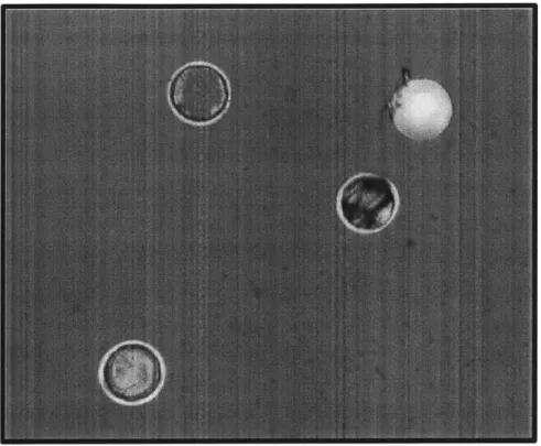
is right side up. The probe tip or vacuum tool contacts the exposed surface of the GaAs layer. The layer of Cr directly in contact with GaAs serves as an adhesion layer for the next Au layer, which is used for ohmic contact. The magnetic Ni layer enables the pill to be used for MASA as well. The bottom Au layer is used for bonding to AuSn pads. The bottom most Cr layer was to promote oxide mask adhesion for a pill processing step, and most of it is sputtered off during reactive ion etching (RIE) to rem ove the oxide m ask...33 3-2 Optopills that have been dispensed on a glass slide: The pill in the top right corner is
bottom side up, with the metal layer facing up, and thus will not be used for MPAP. The rest of the pills in this image are right side up, and thus suitable for MPAP. The semiconductor layer is 35 ptm in diameter while the metal pad is 45gm in diameter. This discrepancy is due to over-etching of the semiconductor layer. This discrepancy is evident in the two "rings" seen on the right-side up pills...34 3-3 Diagram showing how a probe tip is used to pick up an optopill...35
3-4 Schematic of how second probe tip is used to nudge optopill off into recess...38
3-5 Image of optopill placed in a square recess on a silicon CMOS IC chip using solder
flux assisted probe tip M PA P...39 3-6 Image of micropipette attached to micropipette holder...40
3-7 Schematic illustrating how micropipette tip contacts the top surface of an optopill...40
3-8 Micropipette tip designs that were tested (not to scale): a) Tapered micropipette tip. b) Beveled m icropipette tip...42 3-9 Schematic of a pulled micropipette tip that is not tapered or beveled (not to scale).. .43
4-1 Cross-sectional diagram showing initial pressure application method. A weight was placed atop a glass slide that was in turn placed atop the sample to be bonded. The weight was sometime replaced with several glass slides stacked atop the first glass slide... . . .. 4 8
4-2 Schematic of optopill used for bonding using magnetic attraction to hold the pill down (not to scale). These optopills were bonded to recesses that had Cr/Au/Cu/Au
(0.05/0.02/0.5/.02 Rm) pads deposited in them. Note the magnetic layer of Ni
deposited before the AuSn layer...49 4-3 Cross-sectional diagram showing set-up for bonding using magnetic attractive forces
to hold pills down in recesses (not to scale). Note that the substrate chip is smaller than the disc m agnet... 50
4-4 Image of the inner chamber of the vacuum film bonding system. The amber film shown is Thermalimide. The graphite heating strip is visible from the oblong gap in the metal frame supporting the vacuum film...52 4-5 Schematics of vacuum film bonding apparatus design drawn by Prof C. G. Fonstad, Jr.
a) Cross-sectional view of inner and outer chambers. b) Exterior view of bonding apparatus. c) Alternate view of inner and outer chambers...53 4-6 Image of exterior of actual bonding apparatus...54 5-1 Cross-sectional profile of a dummy recess before metal deposition. The metal stack is
deposited atop the polished Si surface (i.e. the recess base)...58 5-2 Phase diagram for Au-Sn system. Taken from
http://web.met.kth.se/dct/pd/element/Au-Sn.html... 59 5-3 Structure of p-i-n diode heterostructures with AuSn layer...60
5-4 SEM image of AuSn coated optopill bonded to HCL cleaned Cr/Au/Cu coated flat Si
substrate. The wider ring of metal around the base of the pill is the melted and reformed AuSn layer that had been deposited on the pill. The pills were held down during bonding using the magnetic attractive force technique...63
5-5 Illustration of AuSn to Cr/Au/Cu/Au metallization structure (not to scale)...64
5-6 SEM image of an AuSn (0.6 gm) pill bonded to a Cr/Au/Cu/Au (0.05/0.02/0.5/0.02
gm) stack. A Ti/Au (0.02/0.2 pm) ohmic ring was successfully patterned on the top
of th e p ill...6 6
5-7 Illustration of Cr/Au to Cr/Au/Sn/Au metallization structure (not to scale). a) No
oxide barrier to prevent Au diffusion into Si. b) An oxide barrier was thermally grown before deposition of the Cr/Au layer to prevent diffusion of Au into Si...69
5-8 SEM images of sample no.1 listed in Table 5-4. Cr/Au/Ni/Au (0.04/0.1/0.25/0.1pgm)
coated dummy optopills were bonded to Ti/AuSn (0.02/0.3 gm) pads deposited in dummy recesses at 360 'C for 10 min using 10 psi of pressure. a) & b) Image of recesses from which bonded optopills had been removed using a probe tip. A striated pattern that was transferred from the optopill can be observed. c) Image of recess that was not filled with a pill during bonding. Balling of the AuSn solder due to the bonding temperatures can be observed. d) A successfully bonded optopill in a recess. The surface roughness on the top of the pill is due to residual AlAs from the etch stop layer that had oxidized... 75
5-9 Image of an array of GaAs optopills taken by J. J. Rumpler. The yellow circles are the
Cr/Au/Ni/Au/Cr metal stacks that had been sputtered on the optopills. The metal stack is missing from one of the optopills in this image. This optopill is identified by the smaller green circle. The discrepancy in the metal stack diameter and the GaAs diameter is due to lateral etching of the GaAs...76
5-10 SEM images of sample no.2 listed in Table 5-4. Cr/Au/Ni/Au (0.04/0.1/0.25/0.1 pm)
coated dummy optopills were bonded to Ti/AuSn (0.02/0.3 gm) pads deposited in dummy recesses at 300 'C for 2 min using 10 psi of pressure. a) Image of recess that was not filled with a pill during bonding. Balling of the AuSn solder can be observed. b) Image of recesses from which bonded optopills had been removed using a probe tip. A striated pattern that was transferred from the optopill can be observed. c) A successfully bonded optopill in a recess. The surface roughness on the top of the pill is due to residual AlAs from the etch stop layer that had oxidized...77
5-11 Illustration of Au to Al/Pt/Au/AuSn/Au bonding scheme...83
5-12 Image of residue covered Cr/Au/Ni/Au optopills dispensed on a glass slide. The gold colored pills are oriented with the metal side up and the silvery colored pills are oriented with the metal side down. The latter pills were selected for MPAP. Most of the pills are covered or surrounded with a fuzzy residue regardless of their orientation ... 85 5-13 Image of a Cr/Au/Ni/Au optopill bonded to a flat substrate coated with
Al/Pt/Au/AuSn/Au. As can be observed of the right edge of this pill, parts of the GaAs pill were broken off when a micropipette tip was used to attempt to dislodge the pill. The pill did not budge after repeated pushing at it with the micropipette tip.
The quartz micropipette tip finally broke during one of these attempts to push the pill out of p lace ... 85 6-1 Schematic summarizing the Au to A1/Pt/Au/AuSn/Au bonding scheme and the
function of each layer of metallization...90
List of Tables
1-1 M aterial Properties of Si, InP and GaAs [3], [4]...19 4-1 Therm alimide M aterial Properties...51
5-1 Summary of results of bonding AuSn coated optopills to Cr/Au/Cu (0.05/0.02/0.5gm) coated flat Si substrates. Apart from the first 2 samples listed in the table, all Si substrates used in these experiments were cleaned in a HCL dip, to remove any Cu oxides due to exposure of the top Cu surface to atmosphere, immediately before pill placement. The pills were held down during bonding using the magnetic attractive force technique. Bonding temperature was ramped up and down at a 50 'C/min rate... 62 5-2 Summary of results of bonding AuSn coated optopills to Cr/Au/Cu/Au (0.05/0.02/0.5/0.02 pm) pads deposited in dummy recesses. The pills were held down onto the bonding pads in the recesses during bonding using the magnetic attractive force technique. Bonding temperature was ramped up and down at a 50 *C /m in rate... 65 5-3 Summary of results of bonding bare n-GaAs optopills to Pd/Sn/Pd (0.1/0.05/0.1 pm) pads deposited in dummy recesses. The optopills were placed using vacuum tool MPAP and all bonding was done using the vacuum film bonding apparatus. Bonding temperature was ramped up and down at a 40 *C/min rate...72 5-4 Summary of results of bonding Cr/Au/Ni/Au (0.04/0.1/0.25/0.1 pm) coated
dummy optopills to Ti/AuSn (0.02/0.3 jim) pads deposited in dummy recesses. Bonding temperatures were ramped at a 40 *C/min rate...74
5-5 Summary of results of pad-to-pad resistance measurements of Al/Pt/Au/AuSn pads in dummy recesses on highly doped (> 1019), low resistivity (0.01-0.02 Q
cm2) Si...79
A-1 M icropipette Cleaning Recipe... 93
Chapter 1
Introduction
1.1. Motivation for Monolithic Optoelectronic Integration
Heterostructure III-V optical devices such as laser diodes and p-i-n detectors are already widely used as fundamental components of common items like fiber communication systems, cellular telephones, and compact disk players. The optoelectronic properties of III-V materials such as indium phosphide (InP) and gallium arsenide (GaAs) are superior to those of silicon. Most III-V materials are direct bandgap and thus electrons in them can make highly efficient optical transitions. Moreover, the physical and chemical III-V material properties can be tuned over a large range to adjust the bandgap, thus providing great flexibility. Using advanced deposition techniques like Molecular Beam Epitaxy (MBE), high quality, low defect III-V material can be grown with the desired bandgap profiles.
Conversely, silicon has an indirect bandgap that results in weak emission and absorption of light, as energy transitions require both photons and phonons. Such multi-particle interactions have a low probability of occurrence compared to the direct electron transitions in direct bandgap materials. This low quantum efficiency renders silicon impractical for optoelectronic applications such as laser diodes.
Nevertheless, while silicon is an unsuitable material for optoelectronic devices, it is an ideal platform for heterogeneous integration with III-V heterostructure devices. This is largely due to the existence of an established, mature high performance integrated circuit technology for silicon. This means that high quality silicon and silicon-on-insulator (SOI) 17
materials are relatively inexpensive to produce in large wafer diameters that ensure a high number of chips per wafer. Moreover, silicon is a better heat-conducting platform than compound semiconductors, and thus may ensure greater power efficiency of devices like lasers and power transistors. Integrating III-V heterostructures onto commercially processed high density Si integrated circuits, such as VLSI and ULSI circuits, thus enables us to reap the benefits of both III-V optoelectronic functionality and the established Si process technology.
For instance, optical interconnections in an optoelectronic integrated circuit (OEIC) can overcome the limitations otherwise imposed by electrical interconnections on the density and speed of integrated circuits, such as high levels of power dissipation and large wire parasitics. This could also increase the available bandwidth of the system and reduce the susceptibility to electromagnetic interference.
However, a technology capable of compact and efficient heterogeneous optoelectronic integration is desired to maximize the potential advantages of such integration.
There are two classifications of optoelectronic integration technology, namely hybrid integration and monolithic integration. Hybrid integration generally consists of integrating III-V optical device circuits and fully processed Si CMOS integrated circuits (ICs) on the same substrate or package. There are several methods, such as wire bonding, to interconnect the distinct chip-level components. Flip-chip bonding and selective thinning of the heterostructure devices are some of the other implementations of hybrid integration technology that have been demonstrated. For instance, vertical-cavity surface-emitting lasers (VCSEL's) have been successfully bonded to high performance CMOS circuits [1] and high electron mobility transistors (HEMT's) selectively thinned for integration without much decrease in device performance [2].
Hybrid integration offers an immediate and relatively simple solution to manufacturing OEIC's while providing some space and package savings and allows for testing of the discrete components before assembly. However, hybrid integration does not allow for the high device densities that are required for high performance OEIC's. Due to 18
the discrete, chip-by-chip nature of such integration, there is minimal cost saving as the labor-intensive manufacturing, testing and interfacing of individual chips does not provide for economies of scale. The processing costs are further heightened by the need for precise alignment when interconnecting individual components, and device complexity and reliability are compromised due to problems like interfacing losses and reflections.
Monolithic integration, on the other hand, refers to the integration of all optoelectronic components on a single chip. Combining all required functionalities on a single unit ensures higher device density and reduced circuit size. Monolithic integration can accommodate higher circuit complexity and promises better system reliability, as the need for alignment sensitive inter-chip connections is eliminated. There is also the advantage of reduced per unit cost, as mass production is possible since the integrated devices can be batch processed on large Si wafers. Hence, in the long run, monolithic integration offers a more cost-effective, scaleable, and therefore practical solution to optoelectronic integration, as compared to hybrid integration.
Material Lattice Constant (A) Coefficient of Thermal Expansion
I_ at 25*C (10-6/*C) at 300K
Si 5.4309 2.6
InP 5.8687 4.75
GaAs 5.6532 6.86
Table 1-1 Material Properties of Si, InP and GaAs [3], [4]
Nevertheless, implementing monolithic integration is not without its challenges. The key obstacles faced by optoelectronic integration are the lattice and thermal expansion mismatch between III-V semiconductors and silicon. Table 1-1 illustrates this mismatch. Traditional approaches to monolithic integration, which usually use direct epitaxy of III-V material on Si substrates, are therefore hindered. This is because the mismatch in the crystallographic structures causes stress in the epitaxial growth, resulting in defects and compromising the quality of the heterostructure device. While the lattice mismatch can be overcome by special techniques such as intermediate buffer layers, the thermal expansion mismatch is a bigger problem [5]. Due to the large difference in the Si and III-V material thermal expansion coefficients, a significant number of defects are 19
introduced when the grown structures are cooled from growth temperatures to room temperature. The material quality and thus device performance is severely limited by such defects.
Therefore, alternative monolithic integration technologies must be developed to ensure that this mode of integration becomes a viable long term solution to optoelectronic integration applications.
1.2. Current Integration Technologies
Various heterogeneous optoelectronic integration techniques have been developed. To provide a better perspective of the progress of optoelectronic integration, some of these techniques are described in this section, along with their advantages and limitations. 1.2.1. Flip Chip Bonding
Flip chip bonding is one of the commercial approaches to hybrid integration. There are several flip chip bonding techniques, such as solder bump flip chip bonding and plate bump flip chip bonding but the general concept remains the same. Conductive bumps are deposited on the bond pads on the device chips to provide an electrical, thermal and mechanical connection between the device die and the substrate IC. The bumps also serve as a spacer between the device die and substrate IC. Solder is then deposited on the bumps. The die is then flipped and aligned face down onto the substrate IC. Static pressure and heat are applied to enable bonding. A non-conductive underfill adhesive is commonly applied between the two bonded chips to improve mechanical strength. Figure 1-1 shows the cross section of a flip-chip bonded device that has epoxy wicked between the two dies to serve as the underfill [1].
Flip chip bonding promises good electrical performance, mechanical robustness, reliability, and also has the advantage of self-alignment. It is more efficient, and has reduced interconnect parasitic effects, compared with wire bonding, another hybrid integration technique [6]. However, it can only be used for integration on a chip-by-chip basis (as opposed to entire wafers) and cannot support batch processing of high density devices, which is desirable for large-scale integration.
Figure 1-1 Schematic of III-V VCSEL flip-chip bonded to Si CMOS circuit. [1] 1.2.2. Wafer Bonding
Wafer bonding utilizes the van der Waals bonds between two highly planarized semiconductor materials or a semiconductor and an insulator, as opposed to the metal-to-metal bonds used in flip chip bonding, to bond two processed wafers. Elevated temperatures (3000C-500*C) and even pressure may be applied to facilitate bond formation. Usually, one of the wafers is subsequently thinned down to remove the original III-V growth substrate and to allow for through-wafer electrical connections [7].
Unlike flip chip bonding, this technique supports wafer-scale integration. However, this advantage is limited by the small III-V material wafer sizes (150 nm for GaAs and 100 nm for InP). The small wafer size is attributed to the brittleness of the compound semiconductors. Wafer bonding is also plagued by the problem of material mismatch. Due to the high temperatures involved in wafer bonding, the mismatch of the thermal expansion coefficients of Si and III-V materials can result in bond failure due to the high stress at the bond interface [8].
1.2.3. Direct Epitaxy
This monolithic technique involves direct epitaxial growth of III-V materials on a silicon substrate using molecular beam epitaxy (MBE) or similar methods. Interfacial stress and strains, due to the material property mismatches cited earlier, lead to reduced
lifetimes and severely affect device performance. Although growing a thick strain relief layer or using buffer layers may alleviate some of these problems, there still remains the need to maintain low growth temperatures [9]. Temperatures of subsequent processing steps are also limited.
1.2.4. Fluidic Self Assembly (FSA)
This is a monolithic integration technique which entails processing devices separately on their growth substrate before etching them free to form "blocks". These blocks correspond to the receptor sites that are etched in the target substrates. The blocks are then suspended in a fluid which is then pumped repeatedly over the target substrate, where the blocks fall into the receptor sites. Blocks that miss the receptor sites are re-circulated and flowed over the target substrate again until the receptor sites are filled [10]. The blocks are bonded to the receptor sites, and the filled target substrate is then planarized and processed monolithically. This technique has almost 100 % yields for large blocks (> 150 gpm on a side), but has limited yields for smaller blocks [11].
1.3. Thesis Organization
This thesis describes the development of the microscale pick-and-place (MPAP) and vacuum film bonding techniques. These techniques are potential solutions to the implementation of an alternative monolithic integration technology, Recess Mounting with Monolithic Metallization (RM3).
Chapter 2 describes the RM3 techniques that have or are being studied. The advantages of Optopill assembly (OPA) and the concept of MPAP are also discussed. The results of the study on MPAP are presented in Chapter 3. Chapter 4 describes the development of a vacuum film, high pressure bonding system for bonding the optopills to pads in the recesses. The justification for various metal bonding stacks used for this purpose and the experimental results of these bonding studies are presented in Chapter 5. Conclusions on the development of MPAP and bonding techniques as well as a discussion of future research possibilities are included in Chapter 6.
1.4. Lab Facilities
The microscale pick and place procedures, bonding experiments and some metal deposition were carried out in Prof. Fonstad's electronics and processing labs respectively. Most of the other fabrication processes were done in the Microsystems Technology Laboratories (MTL), specifically in the Exploratory Materials Laboratory (EML). All SEM images were taken using the Environmental Scanning Electron Microscope (ESEM) in the MIT-Center for Material Science and Engineering (CMSE) Electron Microscopy Shared Experimental Facility (SEF).
Chapter 2
A New Concept
---
Microscale
Pick-and-Place Assembly (MPAP)
2.1. Recess Mounting with Monolithic Metallization (RM 3)
Recess mounting with monolithic metallization (RM3) has been proposed as a means of interfacing optical and electronic device capabilities compactly and efficiently. This integration technology accommodates 111-V heterostructures in recesses etched in commercially processed chips such as Si-CMOS VLSI circuits. These heterostructures are either grown in the recesses, or grown on a separate substrate prior to being positioned in the recesses and subsequently bonded to the IC chips. These recesses are dielectric windows on the IC chips. Subsequently, the chips are processed monolithically to complete the optoelectronic device integration. Figure 2-1 provides a visual of this process. One of the key challenges posed by the implementation of RM is filling the recesses. Previously studied implementations of this technology and their limitations are discussed below.
2.1.1. Previously Investigated Implementations of RM3
Previously studied methods of filling the recesses are Epitaxy-on-Electronics (EoE) and Aligned Pillar Bonding (APB). The EoE technique involves growing III-V heterostructures epitaxially in recesses where the substrate surface in selected areas on fully-processed GaAs integrated circuit wafers are exposed [12]. APB, on the other hand, uses aligned, selective-area bonding to integrate heterostructures onto processed IC 25
wafers. The heterostructures are grown on an optimal substrate wafer using molecular beam epitaxy (MBE), patterned into pillars, then bonded into recesses on the target IC wafer using either fusion or metallurgical bonding. The substrate wafer is then removed by etching. The EoE and APB techniques are described in Figures 2-2 and 2-3 respectively.
Heterostructure
a
-Figure 2-1 Schematic of a RM3 Process: a) Recess etched in commercially processed IC wafer and contact-cum-bonding pads deposited in recesses. b) Device heterostructure
placed or grown in recess. c) Assembled circuits are processed monolithically. One of the key limitations of EoE is that it is only compatible with IC wafers of the same composition as the heterostructures grown on the IC wafers. This is due to the issues of lattice constant and thermal expansion coefficient mismatch that compromise device performance if the IC substrate and heterostructure are of different material composition. EoE is thus less versatile and cannot be applied to Si IC wafers effectively. Moreover, due to the need for a thorough cleaning process when opening the growth recesses to ensure good quality growth, yields are relatively low over the entire die. In addition, the MBE growth temperature is limited to below 475 *C to prevent chip damage [13].
Conversely, APB is compatible with a wider range of IC wafer and alleviates the problems due to thermal expansion coefficient mismatch. This is because the heterostructures and Si circuits are grown or processed optimally on separate substrates. However, it does not allow for efficient use of the epitaxial material, as much of this is etched off during the patterning to form the pillars.
OaA MESFET drcuity with mult-layer interconnects a. Processed GaAs IC as received from th
manufacturer
Polycrystalline deposit MftrmNafer b. After ephaxy and prior C.
* to removal of the poly- pro crystalline deposit
Figure 2-2 Illustration of EoE technique. [14]
onditically integrated surface
milling diode (VCSEL or LED)
Optoelectronic device
cesing and Integration
completed
-Dwieecc wvl
a. The processed IC water as received from MOSIS
a obondftklyern sp
b. The detector water with pillars matching the
windows on the IC wafer.
Figure
-Bondedintedace
c. After alignment and bonding of detector
and IC wafers @uew viet
odi cm6 welln a er iam shown, whees manyM iOhuwmde
are Inlegrtasd uMiUtarnouu*y
In o ProeWng of M wakre)
d. Detector wafer Substrate removed and structure ready for further device processing
Dleftri overod LuiP
e. Processing complete
2-3 Illustration of APB technique. [14]
2.2. Introduction to Microscale Pick-and-Place (MPAP)
The microscale-pick-and-place (MPAP) technique is proposed as an RM3 solution to filling the recesses. This technique seeks to overcome the limitations imposed by EoE and APB on monolithic integration. MPAP is an OptoPill Assembly (OPA) technique used to pick up III-V heterostructure devices in the form of optopills and place them in strategically located recesses on target substrates. Target substrates refer to the IC chips or wafers on which the optoelectronic devices are to be integrated.
The idea of MPAP is to start with developing a manually controlled pick-and-place method first, before refining it into an automated pick-and-place technique that will increase the assembly efficiency manifold. Thus, while MPAP may seem unattractive initially due to its pill-by-pill approach, the potential for mechanization of the process
should be taken into consideration. Further advantages of MPAP are discussed later in this chapter.
Another OPA technique that is concurrently being studied is Magnetically Assisted Statistical Assembly (MASA) [15], [16]. This technique utilizes attractive magnetic forces to assemble the pills in the recesses and will not be discussed further. The optopills used in MPAP and MASA are fabricated using the same process.
The two main steps involved in MPAP, namely optopill fabrication and pick-and-place assembly, are described briefly as follows.
2.2.1. Optopill Fabrication
The optopill fabrication entails growing the heterostructures on a suitable device substrate. The heterostructure material is optimally processed on its growth substrate before being patterned into cylindrical pillars. These cylindrical pillars are termed "optopills". This optopill fabrication process has been developed by J. Rumpler and J. Perkins [15], [16]. GaAs Si 1018 3.5 pm Al.AGa.7 As si 10" 0.3 pm Ga.As be 1018 0.66 pmn AI.3Ga.7 As be 10'8 0.7 pm GaAs be 101" 0.05 pm AlAs be 1018 0.1 m p-type substrate
Figure 2-4 Sample optopill structure (not to scale): an LED grown bottom-side up on p-type substrate. The AlAs layer is a sacrificial layer, and the AlGaAs layers serve as
confining regions on both sides of the GaAs active layer.
Typically, the optopills are MBE grown, bottom-side up, with a sacrificial layer
grown between the actual device and the growth substrate. This layer facilitates etching the optopills free of their substrate. The optopills are then collected on an adhesive such
as a polymer, and placed in a fluid such as a solvent to dissolve the adhesive. The pills in the solution are then dispensed on a flat substrate to be picked up and assembled by MPAP into their target recesses on integrated circuit wafers. Figure 2-4 is an example of an optopill structure described in [16].
2.2.2. Pick-and-Place Assembly of Optopill in Recesses
This step involves manipulating a narrow tipped tool of the order of 20-60 gm in diameter to pick up similarly sized optopills that have been dispensed onto a flat substrate, and place them in their target recesses, as shown by Figure 2-5.
0
a) Optopills dispensed on flat substrate e.g. glass slide
b) OptoPill picked up by narrow tipped tool
c) Optopill placed in recess on target substrate using narrow tipped tool Figure 2-5 Schematic of the MPAP technique.
d;i 4D 4D 4W 4M 4D 4D 4D 4W 4W 4W 4D 40 4W
Two methods of MPAP have been investigated. Both use a micro-manipulator to control the pick-up tool. The first uses a metal probe tip coated with a thin film of liquid to pick up the pills and place them accordingly. The second requires the use a vacuum pick-up tool to assemble the pills. Both techniques will be discussed in detail in the next
chapter.
After the optopills are assembled, they are bonded to metallurgical pads in the recesses on the target wafers. The bonded pills and the target wafers are then processed monolithically.
2.3. Benefits of MPAP
MPAP is a promising monolithic integration technique due to a number of advantages that it has to offer. Firstly, as the heterostructure devices are grown on a separate substrate, they can be grown under optimal conditions on optimum substrates, ensuring high quality device performance. The MBE growth tmperature is not limited by chip tolerances, unlike EoE.
Having a separate device growth substrate means that the target IC substrate wafer size is not restricted by the wafer size typical of the heterostructure material. This enables the use of standard wafer sizes, and is especially advantageous when integrating III-V materials onto Si target ICs, since III-V wafers are typically much smaller than Si wafers. MPAP also provides a greater degree of flexibility, as the optopill structure and material can be varied depending on the heterostructure device functionality required. MPAP can thus be applied to a wide range of optoelectronic integration needs.
Multiple types of heterostructure devices can also be assembled on a single target IC substrate using MPAP, since each type of device can be grown and processed into optopills on separate growth substrates before being integrated. With techniques like MASA and APB, however, assembling multiple types of heterostructures on a single substrate will be difficult as complex modifications have to be made. For instance, performing such integration using MASA may require variation in the shape of the optopills and recesses to ensure the right heterostructure device falls in each target recess. 30
Conversely, no modification to the MPAP technique is required to accommodate this mode of integration. MPAP is thus highly practical for complex optoelectronic designs where more than one type of heterostructure device is desired, as compared to other RM3 techniques.
In addition, the heterostructures can be grown in a densely packed pattern that ensures efficient use of the epitaxial material. While the cylindrical pills are producible in many material systems due to their symmetry, pills of other shapes can also be fabricated using different mask patterns. For instance, square or rectangular p-i-n diode pills may be grown to interface with waveguides. This adds to the versatility of the MPAP technique.
Moreover, MPAP can be used to place heterostructure devices atop existing devices on the target substrate, enabling 3-D circuit capacity. The optopills can also be tested before integration to ensure that working devices are assembled on the target
substrate [16].
Although MPAP may seem tedious, it lays the foundation for future mechanized methods of pill assembly. If adapted into an automated assembly technique of a reasonable efficiency, it may be compatible with wafer batch processing. Thus MPAP is a novel integration technique worth looking into.
Chapter 3
Development of MPAP
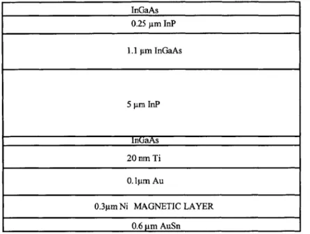
The two MPAP techniques that have been developed will be discussed in this chapter. This study utilized similar optopills to develop both techniques. The optopills used had a thickness of 5 - 6 pm and were 35-50 n in diameter. For this study, the actual composition of the III-V optopills was not as important as the size and shape of the pill. Thus, some of the optopills used had a structure similar to that described in Figure 3-1. These dummy optopills had no actual device functionality but were sufficient for determining the practicality of MPAP. The metal layers were varied depending on the bonding experiments that were conducted using the placed pills. More detail regarding this will be given in Chapters 4 and 5.
5 pm n doped GaAs
-10 nm Cr
-O.pmAu ~ 0.25pm Ni
.ljimAu
10 nm Cr (most of this is sputtered off during RIE)
Figure 3-1 Schematic of typical dummy optopill used in MPAP study (not to scale): The pill here is right side up. The probe tip or vacuum tool contacts the exposed surface of the
GaAs layer. The layer of Cr directly in contact with GaAs serves as an adhesion layer for the next Au layer, which is used for ohmic contact. The magnetic Ni layer enables the pill to be used for MASA as well. The bottom Au layer is used for bonding to AuSn pads. The bottom most Cr layer was to promote oxide mask adhesion for a pill processing step, and most of it is sputtered off during reactive ion etching (RIE) to remove the oxide mask.
These optopills were collected as described in [15], [16], and subsequently dispensed in methanol on either glass slides or pieces of polished Si for MPAP. The optopill fabrication, collection and dispensing were done by J. Perkins and J. Rumpler. Figure 3-2 shows some of these pills that have been dispensed on a glass slide. About 50 to 100 pills were dispensed each time. The pills were picked up by either MPAP method and placed on both flat substrates and recesses etched into substrates like Si or silicon dioxide.
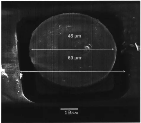
Figure 3-2 Optopills that have been dispensed on a glass slide: The pill in the top right corner is bottom side up, with the metal layer facing up, and thus will not be used for MPAP. The rest of the pills in this image are right side up, and thus suitable for MPAP. The semiconductor layer is 35 gm in diameter while the metal pad is 45pm in diameter. This discrepancy is due to over-etching of the semiconductor layer. This discrepancy is
evident in the two "rings" seen on the right-side up pills. 3.1. Probe Tip MPAP
It was initially observed that a dirty probe tip, when placed on the top surface of an optopill, could be lifted up with the optopill still attached to the probe tip. Thus it was inferred that using either static force or adhesive force, it would be possible to pick-and-place optopills using a probe tip.
The probe tips used had a tip diameter of approximately 10 gm. The fine tip diameter ensured the probe tip did not obscure the optopill and allowed for a good view of the pill during pick-and-place. Before using any probe tip to pick up optopills, it was cleaned with isopropanol. To enable controlled manipulation of the probe tip, the cleaned probe tip was attached to a micromanipulator like those commonly found on manual probe stations.
Using a microscope for visual aid, the probe tip was maneuvered over the glass slide or flat substrate of pills and carefully positioned directly above an optopill. It was then lowered to come into contact with the top surface of a dispensed optopill. Only optopills that were oriented right-side up were selected. This is illustrated in Figure 3-3. A right-side up pill refers to a pill where the metal layers are facing down and in contact with the glass slide or flat substrate, and the semiconductor layer is the top, exposed layer (i.e. the probe tip contacts the semiconductor layer). The pills that were wrong-side up could be rinsed off the flat substrate, recollected in solvent and dispensed again for MPAP to minimize pill wastage.
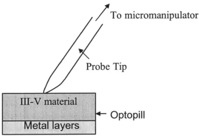
ATo
micromanipulator Probe TipI-V material
Optopill
Metal layers
Figure 3-3 Diagram showing how a probe tip is used to pick up an optopill.
The probe tip was slightly lowered so some pressure was applied on the pill before it was lifted up again. This was repeated until the pill was picked up and attached to the probe tip. The probe tip, with the pill attached, was then moved and lowered onto the target substrate or recess until the bottom surface of the pill was in contact with the target pad. The static forces between the bottom of the pill and the target pad sometimes 35
overcame the adhesive forces between the pill and the probe tip, enabling pill placement. The probe tip could also be lightly moved around to loosen the pill onto the flat substrate or into the recess. If this did not work, another cleaned probe tip was used to nudge the pill off the tip and onto the target pad.
3.1.1. Investigation of Suitable Adhesive Film for Probe Tip MPAP
It was first attempted to use clean probe tips to pick up and place pills using sheer static force. However, this method failed, as the dispensed pills would not adhere to the probe tip and could not be lifted up from both the glass slide and polished Si surfaces. The only way that a pill could be picked up was when the probe tip had dust or dirt on it. This dirt was visible under the microscope. Such levels of contamination would definitely affect any post-assembly processing.
It was therefore concluded that relying on static force alone for MPAP was insufficient, and it would be necessary to apply an adhesive film on the probe tip to aid in pill pick up. It was preferable that this film could be easily removed after pill placement. Several liquids were considered as it was thought that coating a probe tip with a thin film of liquid would provide sufficient adhesive force between the tip and the optopills. A cleaned probe tip was coated with the desired liquid film by dipping it in the respective liquid before being used to pick up the optopills. The liquids tested and the results are discussed in the following subsections. Each liquid was used in at least twenty attempts to pick up pills.
3.1.1.1. Deionized Water
It was hoped that deionized water would serve the purpose of an adhesive film. This was because of its neutral properties and that any deionized water on the top surface of the optopill could be easily removed by a simple evaporation step with little effect on the optopill or the underlying circuitry the pill was placed on. Unfortunately, repeated attempts to pick up optopills using probe tips dipped in deionized water were unsuccessful. The only time a pill could be picked up, after several tries (i.e. the probe tip was lowered into contact with the pill and raised up repeatedly), occurred when an entire 36
drop of water was dripped on the glass slide, wetting all the pills in the area of the water drop. This was not an option for MPAP, as it was not desirable to coat the entire pill in deionized water, and removing liquid between the bottom side of the pill and the pad in the target recess would be a problem.
It was inferred that perhaps a more viscous liquid would provide better adhesive force than deionized water. Two such liquids, photoresist and glycerol, were tested. 3.1.1.2. Photoresist
Two types of photoresist were experimented with under the consideration that photoresist could be easily removed by acetone after MPAP. The first was the thick resist AZ 4620, and the latter was AZ 5214 which is typically used for image reversal photolithography. AZ 4620 was too thick, and messy blobs of resist tended to form on the probe tips, rendering impossible to get a good view of the pills underneath the tips. Conversely, the less viscous AZ 5214 did not provide sufficient adhesive force for the pills to stick to the probe tips.
3.1.1.3. Glycerol
Glycerol was also too viscous and had a tendency to clump up. The surface tensional forces within the glycerol drops were far stronger than the adhesive forces between the pills and the glycerol. Thus the pills could not be picked up effectively. Moreover, there is no easy way to remove glycerol as it is not vaporizable.
It was therefore found that thick, viscous liquids were unsuitable for probe tip MPAP. Water soluble adhesive and two less viscous liquids were tested next.
3.1.1.4. Water Soluble Adhesive
Water soluble adhesive from water soluble tape was transferred onto the probe tip by wiping the tape on the probe tip. It was very easy to pick up the pills as the soluble adhesive provided a strong adhesive force between the pill and the probe tip. However, it was almost impossible to remove a pill from the tip and onto the target substrate or recess
once the pill was stuck to the probe tip. Using a second probe to knock the pills off the first probe and onto the recess did not work effectively either.
3.1.1.5. Pump Oil
Pump oil was used rather successfully as an adhesive film on the probe tips to pick up the optopills. An experiment was done to get an idea of the effectiveness of pump oil as an adhesive film. Attempts were made to pick up 50 optopills from a glass slide using pump oil coated probe tips. Out of the 50 optopills, 27, or 54% of pills were successfully picked up within 2 tries. The rest of the pills were broken during the attempts to pick them up when too much pressure was applied on them via lowering the probe tip.
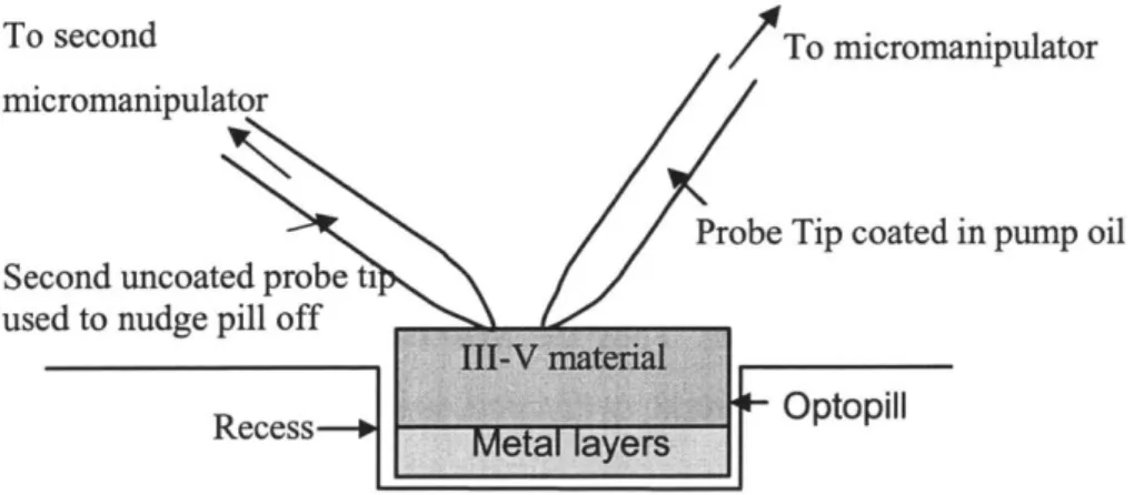
In fact, the pills adhered so well to the probe tip that it was difficult to place them on either flat substrates or in recesses etched in a piece of Si. A second, uncoated probe tip attached to another micromanipulator had to be used to nudge the pills off the pump oil coated probe tip and onto the target pads. This is demonstrated in Figure 3-4.
To second
/To
micromanipulatormicromanipulator
Probe Tip coated in pump oil Second uncoated probe ti
used to nudge pill off
III-V material
Recess0 Metal layers Optopill
Figure 3-4 Schematic of how second probe tip is used to nudge optopill off into recess. However, pump oil is not easily removed, as it cannot be evaporated away. A degreaser could be used to remove the pump oil, but this would require an elaborate set-up and it would be difficult to ensure that the pills stayed in place on the target substrates during degreasing. Moreover, degreasing will involve condensation of the solvent used in the vapor degreaser on the entire chip surface.
3.1.1.6. Solder Flux
An alternative was sought in solder flux. SuperSafe Superior No. 30 liquid solder flux was used. It was found that solder flux was a more effective pick-up adhesive film than the pump oil. While a second probe tip was also needed to assist in placing the pill, less liquid residue was left behind on the top surface of the pill after pill placement. Figure 3-5 shows a pill that had been placed successfully in a recess using solder flux assisted probe tip MPAP. In addition, solder flux becomes completely neutral, electrically non-conductive and non-hygroscopic upon heating properly, and can thus be removed by evaporation.
Figure 3-5 Image of optopill placed in a square recess on a silicon CMOS IC chip using solder flux assisted probe tip MPAP.
Although solder flux provided a relatively cleaner probe tip MPAP solution, there was still concern that some residue would be left behind after evaporating most of the solder flux and an additional step would be required to remove this residue. Moreover, there was a strong tendency for the pills to break during attempts to pick them up. This was due to the pressure that had to be applied by the probe tip for the pill to adhere. A cleaner MPAP process with a more effective mode of pill pick-up was desired.
3.2. Vacuum Tool MPAP
The second technique investigated uses micropipettes with pulled tips as a vacuum pick-up tool in place of the probe tip. These micropipettes are not unlike those used in biological applications such as cell biology. A clean micropipette is attached to a micropipette holder that is connected to a micromanipulator for controlled maneuvering of the micropipettes. This part of the set-up is shown in Figure 3-6.
Figure 3-6 Image of micropipette attached to micropipette holder.
:ropipette
Tip
Figure 3-7 Schematic illustrating how micropipette tip contacts the top surface of an optopill.
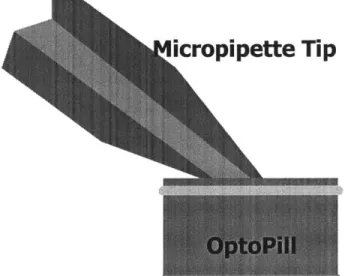
The micropipette is positioned atop dispensed pills that are oriented right-side up, with the micropipette tip directly in contact with the pill surface. This is illustrated in Figure 3-7. The pill is picked up using vacuum pressure. A vacuum pump is hooked up to the micropipette holder to apply this vacuum pressure. The pill is placed onto the target recess (or substrate) either by merely releasing the vacuum pressure to atmospheric pressure or applying a slightly higher positive pressure using a neutral gas like argon. 3.2.1. Determination of Micropipette Tip Design
The first step to developing the vacuum tool MPAP technique was to find a suitably designed micropipette that could serve as an efficient pick-up tool. The initial choices for this purpose were glass micropipettes manufactured by Sutter Instruments. The tips of these micropipettes could be pulled into different shapes and sizes to suit their application. The micropipettes were pulled from 1mm outer diameter (O.D.) by 0.5 mm inner diameter (I.D.) glass tubing. Micropipettes with several variations in their design were experimented with to determine an optimum design for pill pick-and-place.
The first variation was the O.D. of the micropipette tips, from 25 gm to 45 gm. A larger diameter micropipette offered the advantage of a larger rate of flow of gas through the micropipette resulting in a more effective vacuum pressure and was thus preferred. However, it was necessary that the O.D. of the micropipette was smaller than the optopill surface so that the pills could be viewed clearly using a microscope while maneuvering the pipette atop the pill. As the diameter of pills used ranged between 35 to 50 Rm, it was determined that a 35 gm O.D. micropipette tip was the optimum size.
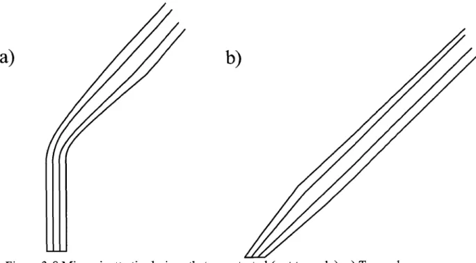
Another variation was the shape and angle of the tip of the pipette. Two designs were tested, one with no taper in the tip and a 45 degree bevel, and the other with a 60 degree taper and a fire polished flat end with no bevel. Figure 3-8 provides a rough sketch of both designs. As the tips of the micropipettes had to be positioned in the micropipette holder such that the flat end of the tip was parallel to the flat substrate on which the pills were dispensed, it was much easier and faster to position the tapered
design. Conversely, the beveled design required much time for adjustment to ensure its edge was horizontal and parallel to the flat.
However, it was also found that the tapered design limited the field of view of the pills as much of the target pill would be blocked by the vertical end of the tapered tip. Moreover, the pipettes with the tapered edge had a longer, finer 10mm tip as opposed to the 8mm tips on the beveled pipettes, and were thus easier to break. Thus the beveled design was ultimately preferred. Nevertheless, the beveled glass micropipettes from Sutter Instruments were still relatively easy to break during handling and pill pick-up, and a harder material was desired.
a)
b)
Figure 3-8 Micropipette tip designs that were tested (not to scale): a) Tapered micropipette tip. b) Beveled micropipette tip.
Quartz micropipettes with 35 pm O.D. tips beveled at 45 degrees from Precision Micro Devices were found to be better suited for MPAP due to their tougher material composition and shorter 6mm pulled tip [17]. These micropipettes were pulled from 1mm O.D. by 0.5 mm I.D. quartz tubing. These quartz micropipettes were used successfully to pick up optopills and place them both on flat substrates and in recesses. There was no pill breakage that occurred during pill pick-up, and the pills could be released from the 42
micropipette tips into their target locations by applying a positive pressure through the micropipettes using argon.
Thus, it was found that using clean quartz micropipettes with a 35 pm O.D. tip beveled at 450 and applying vacuum pressure through the micropipettes, optopills could be assembled onto their target recesses. The amount of vacuum pressure applied at the micropipette tip was measured to be approximately 0.1 atm or 1.5 psi. This vacuum tool MPAP provides a cleaner alternative to probe tip MPAP as no chemicals come in contact with the pills and pill breakage does not pose a problem.
It should be noted here that the micropipette tip design provides a degree of flexibility for various systems. The micropipette tip size may be changed according to the optopill size, and the tip design may be optimized to suit the specific set-up available for vacuum tool MPAP. For instance, if this MPAP technique is to be automated, a straight, non-tapered and non-beveled micropipette tip like that shown in Figure 3-9 may be desired.
Figure 3-9 Schematic of a pulled micropipette tip that is not tapered or beveled (not to scale).
3.2.2. Micropipette Storage and Cleaning Procedures
The micropipettes from Precision Micro Devices were prone to attracting static dust and were water adsorbent. Therefore, care had to be taken during storage of the micropipettes. The micropipettes were kept in a static dissipative case to prevent accumulation of charged particles within the case. The case was stored in a desiccator cabinet when the micropipettes were not in use to minimize the hydration of the glass. When taken out of the cabinet, the case was kept in two layers of ziplock bags with a packet of desiccant between the two bags to adsorb moisture. The ziplock bag helped to keep dust off the case. The desiccant could not be placed directly in contact with the case as the desiccant packet shed.
Despite these measures, the micropipettes tended to attract dust particles and solvent residue (since the optopills had been dispensed in solvent), and adsorb moisture during use for MPAP. A methodical way of cleaning the micropipettes had to be designed in order to enable reuse of the micropipettes.
Personnel at Precision Micro Devices recommended using solvents like acetone or isopropanol to clean the micropipettes. Initial cleaning attempts involved using squirt bottles to project a narrow stream of acetone, methanol and isopropanol through the micropipette. The micropipette was then dried using a nitrogen air gun directed as best as possible down the middle of one end of the micropipette. The micropipettes cleaned this way were examined under a microscope. While the solvent had been successfully evaporated using the air gun, there was still a significant amount of particulates that had not been removed from the micropipette tip. Thus it was determined that the squirt bottle method was insufficient for removing debris from the micropipette tip.
A sonication cleaning method was tried instead. The micropipettes were held by a clamp and suspended in a beaker of acetone. This beaker was positioned in a 40 kHz ultrasonicator and sonicated for 10 minutes. Using squirt bottles, methanol and isopropanol were then squirted around and through the micropipettes. These micropipettes were then blown dry with an air gun in the manner described previously. It was found that this cleaning procedure was able to remove all particulates that were
visible under the microscope from the micropipettes. This sonication and blow dry method was adopted for cleaning the micropipettes for MPAP reuse.
These micropipette storage and cleaning procedures are summarized in Appendix A.
Chapter 4
Vacuum Film Bonding
4.1. Introduction to Optopill-to-Recess Bonding Issues
A technique for bonding the assembled optopills into their target recesses had to be devised. Good quality, robust bonds between the optopills and the recesses are necessary to ensure the optopills stayed in place for post-assembly processing. Ideally, the bond would also provide for a good ohmic contact between the underlying circuitry and the heterostructure device.
There were two main issues that had to be considered when designing this optopill-to-recess bonding technique. One of them was the need for a suitable metallurgical stack that fulfills both optopill-to-recess bond requirements stated above. Several bonding stacks were investigated. While most of these bonding stacks utilized the eutectic AuSn alloy as a soldering agent, a Pd/Sn/Pd stack was also investigated. The results of the study of these bonding stacks will be discussed in Chapter 5.
The other pressing concern was to find a suitable method of applying uniform static pressure on the optopills in recesses during bonding. This static pressure was necessary to promote effective bond formation and improve bond quality, especially for the metallurgical stacks that were being studied. This was evident based on the results presented in [18] - [24]. This chapter discusses the development of a vacuum film bonding system to address this issue.
![Figure 1-1 Schematic of III-V VCSEL flip-chip bonded to Si CMOS circuit. [1]](https://thumb-eu.123doks.com/thumbv2/123doknet/14734012.573729/21.918.265.702.116.398/figure-schematic-iii-vcsel-flip-bonded-cmos-circuit.webp)
![Figure 2-2 Illustration of EoE technique. [14]](https://thumb-eu.123doks.com/thumbv2/123doknet/14734012.573729/27.918.142.784.111.342/figure-illustration-of-eoe-technique.webp)