Designing a Wireless Underwater Optical
Communication System
by
Heather Brundage
B.S. Ocean Engineering
Massachusetts Institute of Technology, 2006 Submitted to the Department of Mechanical Engineering in
Partial Fulfillment of the Requirements for the Degree of Master of Science in Mechanical Engineering
at the
Massachusetts Institute of Technology February 2010
ARCHIVES
MASSACHUSETTS INSThTUTE OF TECHNOLOGYMAY 0
5
2010
LIBRARIES
C February 2010 Heather Brundage. All rights reserved.
The author hereby grants to M.I.T. permission to reproduce and to distribute publicly paper and electronic copies of this thesis document in whole or in part in any way now
known or hereafter created.
Signature of Author ...
Department of Mechanical Engineering January 15, 2010
Il c~ /
Certified by...
C
....
- - Chryssostomos Chryssostomidis Director, MIT Sea Grant College Program Doherty Professor of Ocean Science and Engineering Professor of Mechanical and Ocean Engineering he,y visor
A ccepted by ...
David E. Hardt Chairman, Department Committee on Graduate Studies
Designing a Wireless Underwater Optical
Communication System
by
Heather Brundage
Submitted to the Department of Mechanical Engineering on January 15, 2010, in partial fulfillment of the requirements
for the degree of
Master of Science in Mechanical Engineering
Abstract
Though acoustic modems have long been the default wireless communication method for underwater applications due to their long range, the need for high speed communication has prompted the exploration of non-acoustic methods that have previously been overlooked due to their distance limitations. One scenario that drives this need is the monitoring of deep sea oil wells by AUVs that could be stationed at the well and communicate surveillance data wirelessly to a base station. In this thesis, optical communication using LEDs is presented as an improvement over acoustic modems for scenarios where high speed, but only moderate distances, is required and lower power, less complex communication systems are desired. A super bright blue LED based transmitter system and a blue enhanced photodiode based receiver system were developed and tested with the goal of transmitting data at rates of 1 Mbps over distances of at least 10 meters. Test results in a fresh water tow tank showed the successful transmission of large data files over a distance of 13 meters and at transmission rates of at least 3 Mbps. With an improved test environment, even better performance may be possible.
Thesis Supervisor: Chryssostomos Chryssostomidis Title: Director, MIT Sea Grant College Program
Doherty Professor of Ocean Science and Engineering Professor of Mechanical and Ocean Engineering
Acknowledgments
This work was supported by a National Defense Science and Engineering Graduate fellowship, in connection with the Office of Naval Research, as well as the MIT Sea Grant Collage program. Without their support, this project would not have been possible.
I would like to thank my advisor, Dr. Chrys Chryssostomidis, for giving me the support and freedom to explore fun and challenging projects.
Dr. Milica Stojanovic for being my unofficial advisor and consultant on all things communications-related.
Professor Steve Leeb, and his knowledgeable grad students, for generously contributing their time and resources to assist me in the design of the optical transmitter.
"The boys" of the AUV Lab (Justin Eskesen, Ian Katz, Seth Newburg, Mike Soroka) and Sarah Hammond for helping me in so many aspects of this project, putting up with my clutter and providing camaraderie.
Janice Ahern, Nancy Adams, Trudi Walters and Kathy de Zengotita for handling all the logistics, accounting, scheduling, and other innumerable pieces of the puzzle that made this project
possible and couldn't have happened without them! Norman Farr for a mid-thesis sanity check.
Alex Hornstein for late nights coding, a sympathetic ear, and providing me with the right tools for the job.
Friends and family for their support and encouragement.
and Michael Davis for reading through thesis drafts every day for a month, being a
troubleshooting expert, making sure I didn't drown in the tow tank, helping with circuit board layouts, making fantastic suggestions, keeping me company on late nights and long weekends in lab, providing immeasurable emotional support, and, in general, helping me and this project arrive at the finish line in good, working order.
List of Figures
Figure 1 Absorption coefficient of electromagnetic radiation at various wavelength (8)... 11
Figure 2 Absorption coefficients of visible light wavelengths (9) ... 11
Figure 3 Wireless optical communication system overview ... 13
Figure 4 Transmitter System Overview... 14
Figure 5 LE D Schem atic... 15
Figure 6 Laser diode diagram (24)... 16
Figure 7 TitanTM Series LED Lighting System (1 1)... 19
Figure 8 Signal beam width of LEDs with the narrow beam (110) lens at various distances. ... 20
Figure 9 MOSFET schematic diagram ... 21
Figure 10 Transmitter schematic ... 22
Figure 11 Channel 1 (bottom trace) shows the MOSFET gate voltage when being driven directly from a signal generator producing a 0-5 V square wave. ... 23
Figure 12 Channel 2 (blue trace) in both (a) and (b), which is zoomed in, show the MOSFET gate being driven by an IR2151 which is receiving a square wave signal from a signal generator (Channel 1, orange). ... 24
Figure 13 Channel 2 (blue trace) shows MOSFET gate voltage being driven by the TC4427 M O SFE T driver... 24
Figure 14 TTL232R USB-TTL Level Serial Converter Cable from FDTI ... 25
Figure 15 Schmitt inverter and truth table (31) ... 26
Figure 16 Transmitter system ... 26
Figure 17 Testing the transmitter design. ... 27
Figure 18 Oscilloscope test probe locations for the subsequent screen grabs... 28
Figure 19 Initial transm itter tests ... 28
Figure 20 Improved transmitter testing... 29
Figure 21 Wire-wound (a) vs. Ceramic (b) current-limiting resistors... 30
Figure 22 Final breadboard testing, the blue disks are 1 ohm ceramic resistors. ... 30
Figure 23 Final transmitter testing with inverter added to the PCB ... 31
Figure 24 Transmitter PCB mechanical layout... 32
Figure 25 Populated transmitter printed circuit board ... 32
Figure 26 Receiver system diagram... 33
Figure 27 Photoresistor symbol ... 33
Figure 28 Photothyristor symbol ... 34
Figure 29 Phototransistor symbol... 34
Figure 30 Picture of a photomultiplier (20)... 35
Figure 31 Spectral response of various photodiodes (39)... 38
F igure 32 P C 10-6B ... 38
Figure 33 Receiver electrical system diagram... 39
Figure 34 Basic passive current-to-voltage converter ... 40
Figure 35 Transimpedance Amplifier... 41
Figure 36 Transimpedance amplifier feedback resistor testing ... 42
Figure 37 Output of transimpedance amplifier when Cf is too large... 43
Figure 38 Tuning Cf (a) Cf too small (b) Cf just right (c) Cf too large... 43
Figure 40 Comparing two different voltage amplifiers (a) LM318 (b) LM7171 ... 44
Figure 41 Comparator input (top) vs output (bottom)... 46
Figure 42 Op-Amp Comparator Schematic ... 46
Figure 43 Receiver breadboard testing ... 47
Figure 44 Ringing is present in the receiver circuit while testing on the breadboard. ... 47
Figure 45 Receiver printed circuit board layout ... 48
Figure 46 Back side of the receiver printed circuit board with components ... 48
Figure 47 Receiver testing with the PCB (a) 1 Mbps (b) 3 Mbps ... 49
Figure 48 W ater testing set up ... 50
Figure 49 Transm itter water test set-up ... 51
Figure 50 Receiver water testing m ount ... 52
Figure 52 Com plete receiver test set-up ... 53
Figure 51 Semi-submerged receiver mounted in the tank ... 53
Figure 53 Aligning the transmitter and receiver ... 54
Figure 54 Testing sending/receiving capabilities without the optical link ... 55
Figure 55 30 KB JPEG file transmitted through cable (a) 1 Mbps (b) 2 Mbps (c) 3 Mbps ... 56
Figure 56 Graph of received signal strength at various transmission distances ... 56
Figure 57 Received data at 1 Mbps over 13 meters... 57
Figure 58 Testing at the distance limits of the system (a) 15 meters (b) 16.2 meters ... 58
Figure 59 (a) Original file (b) transmitted at 1 Mbps and (c) 3 Mbps over the optical link... 58
Figure 60 Received data signal at (a) 1 Mbps (b) 2 Mbps (c) 3 Mbps ... 59
Figure 61 Bubbles on the face of the glass in front of the transmitter... 59
List of Tables
Table 1 Comparison of various underwater acoustic modems (4)(5)(6)... 10Table 2 Comparison of LEDs and Laser Diodes (21)(23)(20)(22)(24)(25) ... 17
Table 3 A comparision of high-powered LEDs on the market... 18
Table of Contents
1 Introduction... 7
2 Background ... 9
2.1 W ireless Communication M ethods ... 9
2.1.1 Acoustics... 9
2.1.2 Electrom agnetic W aves ... 10
2.2 Design Constraints ... 12
3 System Design ... 13
3.1 Optical Transm itter ... 14
3.1.1 Photon Source ... 15
3.1.2 LED Driver ... 20
3.1.3 Data Signal... 25
3.1.4 Testing the Transm itter System ... 26
3.1.5 Finalizing the Transm itter System ... 30
3.2 Optical Receiver... 33
3.2.1 Photon Detector ... 33
3.2.2 Signal Processing ... 39
3.2.3 Receiver Testing ... 46
4 System W ater Testing ... 49
4.1 Setup... 49 4.1.1 Transm itter... 50 4.1.2 Receiver ... 52 4.1.3 Alignm ent ... 54 4.2 Testing... 54 4.3 Results ... 56 5 Conclusion ... 60 6 Bibliography ... 61 Appendix... 64
1 Introduction
A major driver of technology is to create machines that can perform tasks in place of humans. Whether the task is too repetitive and boring, requires more precision, or is too dangerous for a person to perform, a robotic system can provide the solution. Though people are no longer able to, or no longer wish to, perform a task, the state of artificial intelligence has not progressed to a point where people are comfortable being completely removed from the loop. Robotic operators still need to communicate with their machines to various degrees - sometimes to completely control them, other times to monitor progress or review data collected from
sensors.
The easiest technological way to communicate with a robot is through a physical connection, such as a copper or fiber optic tether. Though this allows for efficient and high-speed communication, a tether provides many operational challenges when dealing with a mobile robot, limiting the range and maneuverability of the vehicle, as well as requiring an often cumbersome tether management system. For these reasons, wireless communication is a much more feasible solution to the problem of communicating with robotic vehicles. In aerial and terrestrial applications, radio and satellite communications provide adequate speed and range. Underwater environments, on the other hand, have a much greater challenge in achieving wireless communication, while at the same time requiring wireless communication even more.
Since humans are limited in their ability to work underwater, remotely operated vehicles (ROVs) and autonomous underwater vehicles (AUVs) have been in service since the 1950's (1)(2) to perform underwater tasks, such as collecting data and retrieving items. Operation of these vehicles is challenging, but as oil resources are found further off shore, ROVs and AUVs are required to go deeper and stay deployed longer in order to perform critical tasks. One such task is monitoring a deep sea oil well - sending tethered ROV's thousands of meters below the surface in order to conduct surveys is expensive and time consuming! It costs on the order of $100,000 a day to operate an ROV, which can take two hours to dive to the bottom at 3000 meters. This hefty price tag is due to the many expenses including the cost of the boat, the crew, the ROV, and the ROV support team.
A cheaper alternative is to remove the boat and crew from the equation by leaving an AUV stationed at the well, able to charge and communicate with the surface and monitor the well as needed. This would greatly reduce the operational costs involved with current well monitoring and be a much more time and resource efficient approach. In this scenario, a tethered connection between the base station and the AUV would greatly limit the AUVs ability to maneuver. On the other hand, any sort of docking situation requiring a wet-mateable connection would degrade rapidly after hundreds cycles, making it unreliable for long term deployment. In this case, wireless data transfer is required to provide the cost saving benefits of stationing an AUV at a well head. The wireless communication method must be able to support data rates high enough to upload video and other sensor data. Thankfully, long distances are not required, since the AUV could dock or hover anywhere from .1-10 meters from the base station. Power usage and overall size need to be taken into consideration, since the AUV will be running off batteries.
In this paper, I will present a solution to the need for low-power, cost effective, high-speed wireless communication. In the next section, I will compare possible wireless communication methods, present an overview of past work in this area, and cover necessary background information. In the third section, I will present my design and the rationale behind key decisions. In the fourth section I will present data from system tests and in the fifth section I will review the system performance.
2 Background
2.1 Wireless Communication Methods
There are two main mediums by which data can be transmitted wirelessly - acoustic waves and electromagnetic waves. Both of these are used extensively in terrestrial applications. Humans take advantage of wireless acoustic transmission when speaking to one another, while radios work thanks to electromagnetic transmission. In the next few sections, I will discuss how these methods are suited for underwater wireless communication.
2.1.1 Acoustics
Though sound travels decently through air, it travels much better through water. The speed of sound in water is about 1500 m/s, compared to the approximately 340 m/s it travels in air. But the speed at which sound travels through water is highly dependent on the temperature, pressure and salinity of the water. As a result, the presence of thermoclines (temperature gradients) and haloclines (salinity gradients) in the ocean cause acoustic waves to refract when encountering these boundaries. This can drastically change the direction the sound is moving in, or even
channel the sound and propagate it long distances (thousands of meters).
Though some sounds can travel remarkable distances, higher frequency sound is attenuated much faster than lower frequency sound (3). This presents a trade-off between communication speed (high frequency acoustic signals allow for higher data transfer rates) and distance (lower frequency acoustic signals can travel further). This can be seen in Table 1, which compares various acoustic modems. A general trend is obvious in the table: as distance increases, data rate and transmission frequency go down, while size and power increase.
You can see from the table that the fastest acoustic modems can only transmit at data rates of less than a couple hundred kilobits per second. Though this works okay for commands, it is too slow to deal with video. Also, since sound propagates so well underwater, it means there can be a lot of acoustic "noise" in the channel, making it harder to receive a clean signal that doesn't get lost in the noise. This is especially true at deep sea well heads which can be very noisy. Though acoustic modems have their uses and are the only way to send a wireless signal long distances
underwater, acoustic wireless transmission is not ideal for this application which requires high speeds over short distances.
Distance Data Rate Center Frequency Power Weight in Air
Model (m) (kbps) (kHz) (Watts) (kg)
Link Quest UWM1000 350 17.8 35 1 4.2
Link Quest UWM2000 1500 17.8 35 4 5.1
Link Quest UWM3000 3000 5 10 12 6.7
LinkQuest UWM4000 4000 8.5 17 7 8.2 HERMES 120 150 310 32 Evo Logics S2C R 48/78 2000 28 63 80 6.5 Evo Logics S2C R 40/80 2500 33 65 80 6.5 Evo Logics S2C R 18/34 4500 14 24 80 6.5 Evo Logics S2C R 12/22 8000 10 17 80 7.4 Evo Logics S2C R 8/16 10000 6.5 12 80 7.8
Table 1 Comparison of various underwater acoustic modems (4)(5)(6)
2.1.2 Electromagnetic Waves
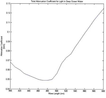
A much faster communication medium is electromagnetic waves. These waves travel at the speed of light, ~300,000,000 meters/second, which is about 200,000 times faster than sound travels through water! Electromagnetic waves are also unaffected by salinity, temperature and depth. Unfortunately, all electromagnetic waves are highly attenuated in water, meaning the signal cannot go very far. This is due to both absorption and scattering. Figure 1 shows the absorption of different wavelengths. You can see that blue optical light is attenuated the least of all electromagnetic radiation. The exact wave length that penetrates the furthest through sea water depends on the characteristics of the specific water, since absorption and scattering is influenced by the chemical and biological make up of the water, but in general wave lengths in the 470nm range at attenuated the least (7). You can see this in Figure 2, which shows the same data as in Figure 1, but zoomed in to only the visible light spectrum.
if I I
100 nm 1000 nm
cm1 1000 cmli i I4 100 cnVli 1 10 cnV1
l l 1 1 1 1
1mm
Figure 1 Absorption coefficient of electromagnetic radiation at various wavelength (8)
Total Attenuation Coefficient for Light In Deep Ocean Water
0.13 0.12 -0.11 0.1 0.09 -0.08 -0.07 --0.06 --0.05 - -D.04 1 1 --L 1 400 420 44 6 8 0 520 50 50 580 60 Wave Length (nm)
Figure 2 Absorption coefficients of visible light wavelengths (9)
11 106 E 105 S104 103 C .2100 o 10 0.1 0.01 10.3 10-6 ... ... ...
- -
-
-cm'
1
00 M 100 cm'11 10 cm'11 10 PM 0 PM WavelengthEven though blue visible light propagates the furthest in sea water, some people have tried using radio waves for wireless underwater communication. RF communications require large and specially designed antennas, above or below water. Wireless Fibre is one company that is currently selling wireless RF underwater systems which they claim can transmit data at 100 kbps over tens of meters (10). Though there are situations where RF communication could be beneficial, the speeds are still too slow for this application and the required antenna size is too large.
Noticing the dip in absorption illustrated in Figure 2, many people have explored using blue light to wirelessly transmit data underwater. In 1995, Bales and Chryssostomidis proposed LED wireless underwater optical communications systems that could theoretically transmit 10 Mbps over a range of 20 meters or 1 Mbps over a range of 30 meters (11). Giles and Bankman take that further in 2005 by calculating theoretical transmission distances for 220 kbps and 4.4 Mbps data rates in various types of water, suggesting the range can vary from less than 10m to over 25m (12). In 2006, Farr et al did preliminary testing with an omni-directional LED communication system and extrapolated to hypothesize that in the future, 10 MHz transmissions could be possible over distances of 100 meter (13). Using lasers instead of LEDs, Hanson and Radic demonstrated 1 Gbps communication over 2 meters in a laboratory water pipe in 2007 (14) and a commercial company, Ambalux Corporation, currently sells a laser-based optical communication system they claim can transmit at 10Mbps over 40 meters (15).
In optimizing for specific design criteria, other researchers have demonstrated impressive results in communication distance and speed. Many have reported transmission speeds in the hundreds of kilobits per second range, over distances of up to five meters (16)(17). More recently, Doniec et al reported 1.2Mbps transmission over 30 meters (18).
2.2 Design Constraints
The previous research shows that underwater wireless optical communication could be a viable solution to the problem of an AUV needing to communicate with a base station at a deep sea oil well head. However, this scenario does impose some specialized design constraints on the system. Mainly, that the system will need to be integrated into a space- and power-limited AUV.
This means that the system needs to use minimal power and take up minimal space. It also means that the system needs to work even without perfect alignment of the transmitter and receiver, since the hovering AUV cannot hold a position without some margin of error. Since the AUV will be deployed and therefore not easily accessible by repair and maintenance crews for a long period of time, a simple system that requires little to no maintenance and has a minimal probability of failure is preferred. Finally, the communication system needs to be high speed (>=1 Mbps) and transmit as far as possible. These priorities - high speed, low power, small size, low complexity, and maximum distance - are what must drive the system design.
3 System Design
A wireless optical communication system is made up of a couple key components (see Figure 3). The computer (be it a laptop or a microprocessor) sends data to the transmitter which converts the electrical signal into an optical signal. That signal passes through the transmission medium (in this case, water) and is picked up by the receiver. The receiver detects the optical signal, converts it back into an electrical signal and passes that data back to the receiving computer.
Receiver 101
Binary Data
Figure 3 Wireless optical communication system overview
There are many different ways light can carry data, but the simplest way is called on-off keying (OOK). In OOK, a binary one is represented as the light being on, and a binary zero is represented by the light being off. This means that the transmitter must be able to read in binary data and quickly and accurately change the state of the optical component accordingly. On the
101- Transmiter
Binary Data
other end, the receiver use a photodetector to determine if the light is on or off and outputs binary ones and zeros accordingly. The speed and reliability of the system is determined by how fast the transmitter can switch the state of the optical component and how quickly and accurately the receiver can determine the state of the light. In the following section, I will describe each subsystem in detail.
3.1 Optical Transmitter
The optical transmitter converts the electrical data signal into an optical signal and projects that optical signal into the transmission channel. It consists of the photon source, which acts as the electro-optical converter, as well as auxiliary systems required to operate and condition the photon source. Figure 4 shows a typical optical transmitter consisting of the input signal, the
optical driver system, the photon source, and any light-beam conditioning optics required, such as reflectors and lenses.
Photon
Source Optical Data Driver- -SystemBeam
Conditioning
Optics
Figure 4 Transmitter System Overview
When designing an optical transmitter, the first step is to decide on your photon source, as the rest of the transmitter is designed to support the selected photon source. In order to determine the best photon source for a system, the available sources must be compared in terms of the goals and constraints on the system, as described in section 2.2.
3.1.1 Photon Source
Selecting the photon source drives the design of the rest of the optical transmitter. Though any photon source, from an incandescent lamp to a laser, could be used, the size, power and switching speed constraints placed on the system narrowed down the selection to two feasible choices: light emitting diodes (LEDs) and laser diodes (LDs). As is to be expected, there are tradeoffs between switching speed, system complexity, and system cost.
3.1.1.1 Light Emitting Diodes (LEDs)
Light emitting diodes (LEDs) are pn-junction
semiconductors that emit visible or infrared light when Anode Cathode forward biased - when the anode is more positive than
the cathode (see schematic in Figure 5). Like regular
pn-junction diodes, LEDs are made from n-type Figure 5 LED Schematic (negative) and p-type (positive) silicon joined together
so that excited electrons on the n side can cross the pn-junction to combine with holes on the p side. The difference is that LEDs are designed in such a way that when electrons combine with holes, they release their energy as emitted photons (19). This random recombination creates spontaneous emission, which emits incoherent light, meaning the photons do not have a constant phase relation (20). Additionally, since photons are released only when electrons recombine with holes, if more electrons and holes recombine, then more photons are released. This means that light output of LEDs is linearly proportional to the drive current.
Unlike incandescent bulbs, which give off many wavelengths of light thereby producing white light, LEDs emit specific colors of light. The wavelength of the emitted photons (the color of light emitted) is determined by the band gap of the semiconductor. The width of the output spectrum (the variation in the wavelengths emitted) can vary upwards of 50nm around that center wavelength dictated by the band gap. Since water absorbs many wavelengths, it is beneficial to use a light source that only produces photons in the -470 nm (blue light) range, as discussed in Section 2.
The switching speed of an LED is determined by its recombination time constant. Depending on the design, the rise time can vary from 1 to 1 OOns (21), meaning LEDs can reach modulation speeds of up to hundreds of MHz.
Though LEDs are affected by extreme heat - they can become non-linear, reduce efficiency and even fail (20) - they are generally highly efficient, stable, and reliable light sources that have a long life time. Because of their simplicity and reliability, LEDs are relatively cheap and widely available.
3.1.1.2 Laser Diodes (LDs)
Laser diodes are similar to LEDs, in that Lens +ve terminal
they are built on pn-junctions (see Figure junction
6), but they are modified to allow the spontaneously emitted photons to cause other electron-hole pairs to recombine.
These photon-induced recombinations Lght emerqes tn
frm Liens +ve terminal
emit photons with the same energy, end
frequency and phase as the incident Figure 6 Laser diode diagram (24) photon that caused them. This is called
stimulated emission and results in coherent light. Stimulated emission occurs only after a threshold current has been reached. It has a much lower recombination time constant, and therefore laser diodes have a much faster rise time, allowing for modulation bandwidths in the GHz range (20). It also results in high optical power emissions in a very narrow optical spectrum width, around 1 nm (19).
Unfortunately, stimulated emission is challenging to maintain. Laser diodes are very sensitive to changes in temperature and current - the wavelength of the laser diode can change by about 0. 1nm/*C (22) and the efficiency and threshold current can change significantly due to age and temperature (20). Thermal, optical and electrical feedback is necessary to sustain operation and prevent the laser diode from failing. This adds complexity and cost to the system. The sensitivity of laser diodes results in shorter life times and lower reliability.
-3.1.1.3 Photon Source Selection
As the previous sections have shown, the choice between LEDs and Laser Diodes is complicated. Table 2 gives an overview of the findings:
Characteristic LED Laser Diode
Optical Spectral Width 25-100 nm .01 to 5 nm
Modulation Bandwidth <200 MHz > 1 GHz
Minimum Output Beam Wide (about 0.5*) Narrow (about 0.010)
Divergence
Temperature Dependency Little Very temperature dependant
Threshold and temperature
Special Circuitry Required None compensation circuitry
Low, off-the-shelf High, need specialized
Cost components available optics and electronics
Long, with little degradation Medium, power levels
Lifetime of power levels degrade over time
Reliability High, 108 hours Moderate, 105 hours
Coherence Incoherent Coherent
Eye Safety Eye safe Must take precautions
Table 2 Comparison of LEDs and Laser Diodes (21)(23)(20)(22)(24)(25)
Both LEDs and laser diodes have strengths and weaknesses when it comes to underwater free space optical communications. Laser diodes can switch faster and have higher optical power output, but LED systems are cheaper, simpler, and more reliable. Though the coherence and minimal divergence of laser diodes is optimal for optical fiber communication systems, it does not play as big a role in wireless optical communication. Additionally, though laser diodes can switch faster, LEDs can switch fast enough for our application (>=1 MHz). Since the goal is to have a small, cheap, reliable communication system that can handle at least 1 MHz, LEDs were
3.1.1.4 LED Selection
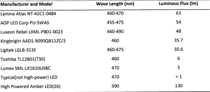
Once the decision was made to use LEDs, the specific LED(s) needed to be selected. Since the goals are to be able to transmit the signal as far as possible, the maximum amount of optical power in the 470 nm range is needed. This can be accomplished by choosing super bright LEDs and by using multiple LEDs. With that in mind, many different LED manufactures were researched to find the brightest blue (~470 nm) LED on the market. Table 3 shows a comparison of various high-power LEDs on the market (all data taken from their respective data sheets). You can see that high power LEDs can give off a luminous flux of 30-60 lumens. This is compared to the less than 1 lumen that standard LEDs produce. Though other colored LEDs, such as Amber, have been around for a long time and are able to produce upwards of 130 lumens per LED, blue LED technology is not as advanced and therefore has a lower lumen output.
Manufacturer and Model Lamina Atlas NT-42C1-0484 AOP LED Corp PU-5WAS Luxeon Rebel LXML-PBO1-0023 Kingbright AAD1-9090QB11ZC/3 Ligitek LGLB-313E
Toshiba TL12B01(T30) Lumex SML-LX1610USBC Typical(not high-power) LED High Powered Amber LED(26)
Wave Length (nm) 460-470 455-475 460-490 460 460-475 460 470 470 590
Luminous Flux (Im)
63 54 48 35.7 30.6 6 5 < 1 130
Table 3 A comparision of high-powered LEDs on the market
High power LEDs generally use 1-5 Watts of power and draw 700-1050mA current, meaning they require a forward voltage of 2-5 volts per LED in series, depending on the LED. In order to maximize light output, more LEDs are desirable, but this must be balanced with the power limitations placed on the system. In this case, the AUV that will carry the transmitter already has a 12 and 24 volt power supply, so it made sense to limit the number of LEDs used so that no more than 24 volts was needed to drive them. Additionally, as more LEDs are added, optical and thermal properties must be taken into account. Though LEDs are not nearly as sensitive to high
temperatures as laser diodes and do not require thermal monitoring, high power LEDs must still be attached to heat sinks to ensure they do not overheat. As more LEDs are added to the system, more or bigger heat sinks are required and all LEDs must be fully thermally coupled to the heat sink. Additionally, since each LED gives off its own light, optics must be used to focus the disparate beams into one beam.
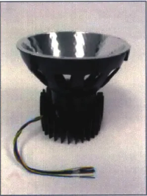
In order to simplify the system and ensure proper operation, it was decided to look for an off-the-shelf lighting engine that incorporated multiple LEDs. Designing specialized optics and heat sinks was not in the scope of this project and the specialized tools necessary to ensure proper thermal coupling between the LEDs and the heat sinks were not available. Though many LED manufacturers make single LED chips, very few integrate them with heat sinks and lenses. Luckily, one company, Lamina Lighting, did just that, and had incredibly bright blue LEDs to boot. Their TitanTM Series LED Lighting System (see Figure 7) uses their Titan blue lighting engine (NT-52B 1-0469), which has seven blue LEDs in series that typically provide 244 lumens at 1 amp and require 19.7 volts (27). It comes assembled with a heat sink, optics (lens and reflector) and wire harness.
Figure 7 TitanTM Series LED Lighting System (11)
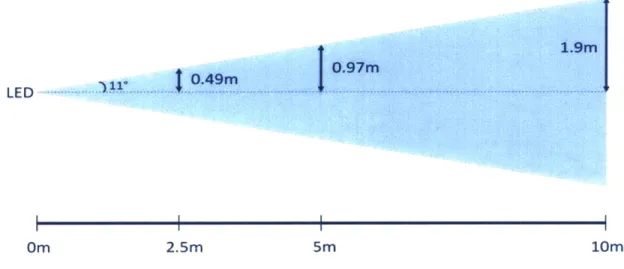
The lens selection also comes down to a trade off. The wider the light beam angle, the less accurately the AUV must hold position while transmitting data. At the same time, the optical signal received is weakened as the beam is widened, since the optical power is spread over a larger area. System constraints, such as the ability of the AUV to hold position within a half meter radius of a specified point and the desire to send the signal as far as possible, rule out the extremes of a single beam of light (like a laser, since the AUV cannot hold a position that tightly while hovering) and an omni-directional light source (since the optical power would be spread ... ... ... ...
further, meaning the distance would be reduced). Additionally, only four lens choices are
available for the Titan lighting system: narrow beam (110), narrow (240), medium beam (350),
and wide beam (480). Figure 8 shows how far the beam would spread over 10 meters when using the narrow beam (110) lens. As you can see, the AUV could hover as close as 2.5 meters away from the base station and still be able to maintain position well enough to complete a transmission. Since the narrow beam lens allowed the AUV to be an acceptable distance away without spreading the beam so far that optical power would be wasted, the narrow beam lens was chosen to be installed on the Titan lighting system.
1.9m
LED
..
I.
Om 2.5m 5m 10M
Figure 8 Signal beam width of LEDs with the narrow beam (110) lens at various distances.
3.1.2 LED Driver
Once the light source was determined, the next step was to design a way to modulate it (turn it on and off) in correlation with the binary data. Since LEDs are current-controlled devices (their output is linearly related to the supply current), a constant current switching power supply would be ideal to maximize efficiency. These are challenging to design from scratch, but there are commercially available constant-current LED drivers. Unfortunately, these are designed for lower speed switching applications, such as LED dimming, and therefore are not optimized for the high speeds optical communications require. No commercial, off-the-shelf LED drivers could be found that could supply the required power (~20 Watts) at the desired speed (>= 1 MHz).
An alternative way of controlling LEDs is to provide a constant voltage (much more common) and limit the current passing through the LEDs using resistors. In this situation, a transistor (an electronically controlled switch) can be used to start and stop the
G
flow of current through the LEDs, turning them on and off. A
metal oxide semiconductor field-effect transistor (MOSFET) is
s
best suited for the job. MOSFETs (see schematic in Figure 9)consist of a drain, gate and source. When there is no voltage Figure 9 MOSFET difference between the gate and the source, there is a very high schematic diagram resistance between the drain and the source so minimal current
flows from the drain to the source - the MOSFET is "off'. If, however, the gate is supplied with a voltage, the drain-source channel becomes less resistive (19) - the MOSFET is "on". Once the gate threshold voltage has been reached, the MOSFET is fully on and the only resistance between the drain and the source is the drain to source on resistance.
MOSFETs are better suited for this application compared to bipolar transistors because they have a much lower drain to source on resistance (milliohms as compared to 10-100 milliohms (19)). This means they will produce a smaller voltage drop and can handle larger currents. Additionally, MOSFETs are better than junction field-effect transistors (JFETs) because they have a much larger gate input impedance (1014 ohms compared to 109 ohms (19)). This means that they draw very little gate current. This is advantageous since the computer or integrated circuit (IC) sending the data signal to the MOSFET typically cannot source a lot of current. If the gate impedance were lower, more current would be needed to change the gate voltage.
Even though the gate impedance is high, there is also a gate capacitance. The larger the gate capacitance, the more current that is needed to charge the gate before the voltage will change. This means that the magnitude of the gate capacitance, and the amount of current that the incoming signal can source, greatly affects that switching speed of the MOSFET. For this reason, MOSFETs that need to switch high power loads very quickly (which is the case in
design) often employ a MOSEFT driver that takes in the data signal and is able to source significantly more current to the MOSFET gate.
There are different types of MOSFETs and MOSFET drivers. For this application, a MOSFET that could quickly switch more than 24 volts at 1 amp was necessary. This means it had to have a drain to source breakdown voltage of at least 50 V and minimal rise and fall time. Additionally, it had to be able to operate from TTL logic levels (0 volts = "0", 5 volts = "1"), which means the gate threshold voltage had to be below 5 volts. After comparing various MOSFETs, the 40N10 was selected. With a drain to source breakdown voltage of 1 OOV and a maximum drain current of 40A, it could more than handle the power requirements of the LEDs. Additionally, its gate threshold voltage is between 2 and 4 volts and it has a very short rise time of 30 ns (28). The TC4427A was selected as the MOSFET driver since it could operate off the 12 V power rail and could drive a high capacitive load very quickly - 1000 pf in 25 ns (29).
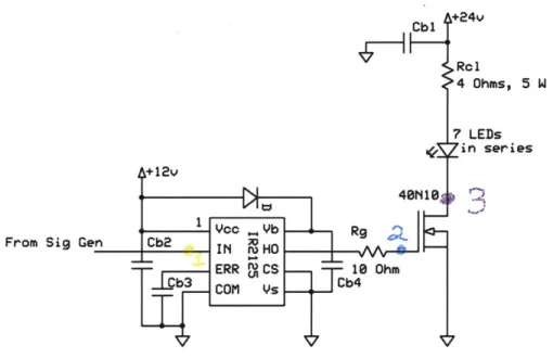
Figure 10 shows the transmitter circuit schematic. The TTL data signal (0-5 V) goes into the TC4427A MOSFET driver which runs off the AUV's 12 volt power rail. The driver controls the MOSFET gate which, when on, allows current to flow through the LEDs and current-limiting resistors which are powered by the AUV's available 24 volt power rail. The 4 ohms of resistance limit the current that flows through the LEDs to 1 amp.
Rcl 4 Ohms in series Data . -Signal In NC NC In A Out A GND £a Vdd In B Out B +12v Cb
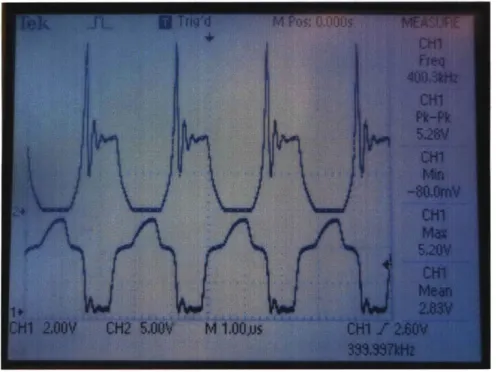
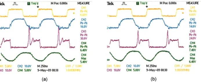
The oscilloscope traces below help illustrate the importance of the MOSFET gate driver in the switching speed of the system. They show the difference between not using a MOSFET driver (Figure 11), using a decent one (Figure 12), and using a better one (Figure 13). Channel 1 (the bottom trace) in Figure 11 shows the voltage on the MOSFET gate when it is being driven directly by a signal generator providing a 400 kHz, 0-5V square wave.
Channel 2 (top trace) shows the drain of the MOSFET. You can see from the figure that it takes over 1 is for the MOSFET gate to reach the full 5 volts the signal generator is trying to drive it to. It is not until the gate voltage passes its threshold that the MOSFET is completely "on" (trace 2 goes to 0 V). While the gate ramps up and down over a period of more than 1 ps, the MOSFET is partially on, allowing limited current through. You can see the results of this on trace 1 where the voltage slopes gently down to 0 volts and then slopes back up. This is undesirable, since it will affect the operation of the LEDs and the resulting optical signal.
Figure 11 Channel 1 (bottom trace) shows the MOSFET gate voltage when being driven directly from a signal generator
producing a 0-5 V square wave.
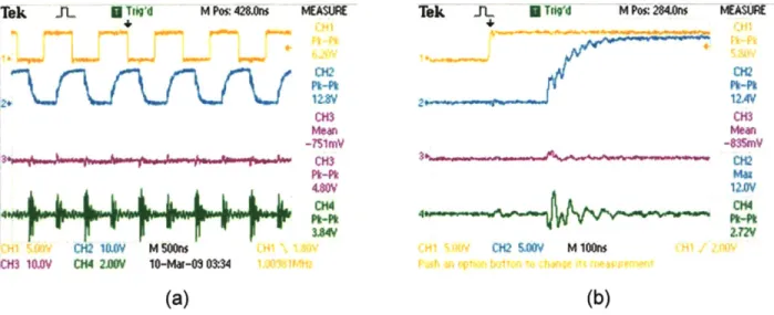
Channel 2 (the blue trace) in Figure 12 (a) and (b) shows the MOSFET gate voltage, but this time, the gate is being driven by an IR2125 MOSFET driver. The IR2125 is receiving a square wave from a signal generator (Channel 1, orange). In the figure, you can see that the gate voltage ramps up to the full signal voltage (in this case, 12 volts) in about 300 ns.
Tek JV *T09d M P0942.Ons MEASUR
Pk-CH2 10."V M50ns C3 10.OV CH4 220V 10-Ma-03 03:34
(a)
Tek JL 0 Tgde M Pos: 24.ns
C12 ft-Pt 12A) V CS3m 014 Pk-ft 013 MW~ ft-ft 4W~ 014 Pt-ft CH2 S0W M100ns
(b)
Figure 12 Channel 2 (blue trace) in both (a) and (b), which is zoomed in, show the MOSFET gate being driven by an IR2151 which is receiving a square wave signal from a signal generator
(Channel 1, orange).
The last trace shows an upgrade from the IR2125 to the TC4427 MOSFET driver. This driver is slightly more powerful than the IR2125 and has a faster rise and fall time. As can be seen in Figure 13, the rise time of the MOSFET gate (trace 2, blue), while being driven by the TC4427, is about 200 ns. This is significantly faster than the 1 is it takes for the MOSFET gate to reach its full voltage with no driver. Additionally, you can see that the drain of the MOSFET (trace 3, purple) has a much better defined "on" and "off', without that slow ramp up and down.
Tek IL a Trig'd M Pos: 0.0005 MEASURE
C H1 CH2 Pk-Pk 2* 16.0V CH3 333,6V CH4 7.OOV ~/~>7~<CH4 4 Max 6.20V H 0 CH2 1V 10.OV M 2SOns FH 1 1M CH3 10.OV CH4 5.00V S-May-03 08:01
Figure 13 Channel 2 (blue trace) shows MOSFET gate voltage being driven by the
TC4427 MOSFET driver.
3.1.3 Data Signal
Once the transmitter had been designed, a way was needed to get binary data from the computer delivered to the MOSFET driver in TTL levels (0 volts = "0". +5 volts = "1"). The communication protocol used (hand shaking, initialization packets, etc) is irrelevant, since it will just be passed through the optical transmitter system and returned to binary data on the receiver
end. The only issue is getting computer output data into TLL levels.
The computer on the AUV has excess USB ports available. Since the USB can handle communication rates of at least 1 Mbps and it also works well for bench testing with a laptop, it was decided to use USB to interface with the computer. USB uses its own protocol to transmit data, with specific synchronization sequences, packet sizes, and end-of-packet indicators. As mentioned above, these protocol specifics do not matter, since they will be passed through the optical transmitter like any other data. What is important is how binary zeros and ones are indicated. USB uses differential voltages, sent over a twisted pair cable, to communicate. A "1" is received when the D+ line is 200mV greater than the D- line, and a "0" is received when the D+ line is 200 mV less than the D- line (30). USB uses a specific communication protocol. Since this is not how TTL logic works, a USB-TTL converter was needed.
The FT232R USB-TTL level serial converter cable does just that. It uses a FT232RQ chip, housed within a USB connector, to turn USB data into asynchronous serial data at TTL levels. In RS232 serial communication, a binary "1" is represented by a negative voltage and a binary "0" is represented by a positive voltage. This means that when the serial data gets shifted to TTL levels in the cable, a logical
"0" is +5 volts and a logical "1" is zero volts. This Figure 14 TTL232R USB-TTL Level reversal doesn't matter to the transmitter, but in an Serial Converter Cable from FDTI effort to conserve system battery energy and prevent
the LED from overheating, a 74HC14 inverting Schmitt trigger was placed between the cable and the MOSFET driver to reverse the values. This means that a logical "0" is again represented
by 0 volts and a logical "1" is represented by +5 volts (see Figure 15 for Schmitt inverter schematic symbol and truth table). Without the inverter, the logical "0" of a dead line (no communication) would be represented by +5 volts, which would turn the MOSFET "on" and the LEDs would be constantly illuminated while idle, draining the battery!
Input Output
Input output
1 0
0 1-1
Figure 15 Schmitt inverter and truth table (31)
3.1.4 Testing the Transmitter System
Figure 16 shows the assembled transmitter system. Data is sent from the computer through a USB-TTL converter cable to the LED driver (which consists of the power MOSFET and
MOSFET driver) that switches the Titan series LED lighting system on and off.
Data
USB to TTL
LED Driver
TitanTM Lighting System
Figure 16 Transmitter system
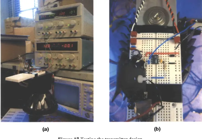
Once this was assembled, the LED driver circuit (see Figure 10) was constructed on a breadboard and the transmitter system was tested to assess performance. Figure 17 shows the test setup. The first picture (a) shows the LED lamp mounted on a metal bar so as to overhang the ledge. The bread board -close up in picture (b) - is attached to the top of the metal bar and two power supplies are used to provide +12V (for the MOSEFT driver) and +24V (to power the LEDs). What can't be seen in either picture is the signal generator that created the square wave input signal to the circuit (taking the place of the computer and USB-TTL converter cable in
initial testing). Since the USB-TTL converter cable was not used in initial testing, the 74HC14 inverter was unnecessary and therefore not hooked up to the LED driver circuit.
(a) (b)
Figure 17 Testing the transmitter design.
In order to understand the transmitter's ability to communicate at various data rates, the signal generator drove the transmitter with various speed square waves while the input signal (from the signal generator), the gate voltage and drain voltage were monitored on an oscilloscope (also not pictured). In the following oscilloscope screen shots: trace 1 (orange) is the signal generator input signal to the MOSFET driver; trace 2 (blue) is the voltage at the MOSFET gate; trace 3 (purple) is the drain of the MOSFET, when the MOSFET is "off' the drain voltage is high, when the MOSEFT is "on", current is allowed to flow through the MOSFET, connecting the drain pin to the source pin, which is tied to ground; and trace 4 (green) is not relevant to the discussion. See Figure 18 for the oscilloscope probe placements as they correspond to the oscilloscope screen print trace number and color.
+Cb1 24v Rol 4 Ohms, 5 W 7 LEDs in series i+ 12v 40IN10 p 1Vc _ Vb RgQ
From Sig Gen Cb2 I H0
-- ERR rO CS 10 Ohm
COM Vs Cb
Figure 18 Oscilloscope test probe locations for the subsequent screen grabs.
When the system was first tested, there were only a couple of basic bypass caps in the circuit and the current-limiting resistor was a single 4 ohm, wire wound resistor that was found in the lab. Between the parasitic inductance and capacitance in the resistor and the parasitic capacitance in inherent in the LEDs, an LC circuit was unintentionally created. As a result, when the MOSFET switched states, turning on and off 24 watts of power, the system experienced significant ringing.
This can be seen in Figure 19. In this instance Tek LU a Trig'd M Pos: 42&Ons MASURE
only, trace 4 (green) is the ground rail and the 2125 MOSFET driver is being used. In this
the2+ 16.OV
test, the signal generator is driving the CH3
Wean
transmitter at 1 MHz. You can see that the 4.37V
2125 MOSFET driver takes a significant
amount
of time toramp
arriunt up the gate voltage (as ampPk-Pk CH48.20V
discussed in section 3.1.2). Additionally, you CH2 1 oov M 500ns
CH3 10.OV CH4 5.O0V 1 0-Mar-03 03:13 7 , H,
can see the incredible amount of ringing in the
system, especially when the MOSFET turns Figure 19 Initial transmitter tests "6off' and the drain voltage spikes to over 35
volts! This ringing affects the entire system, not just the 24 V power rail, as can be expressly noted by looking at the 8.2 peak-peak voltage seen on the ground rail in trace 4.
In order to reduce this ringing a couple steps were taken. The first was to switch out the single 4 ohm wire-wound resistor for four 1 ohm ceramic resistors in series. This change from using wire-wound to ceramic resistors drastically decreased the parasitic inductance in the resistor, since current was no longer flowing through a coiled wire. Additionally, switching from a single resistor to four smaller resistors reduced the parasitic capacitance. This happens because though resistors add when placed in series, capacitors in series result in a total capacitance that is less than any single capacitor in series (see Equation 1).
1 1 1 1
CT C1 C2 Cn
Equation 1 Capacitors in Series
Finally, more appropriate and more total by-pass capacitors were used between the 24 volt supply and ground. Large value electrolytic by-pass caps (1000p1f) were replaced with low ESR capacitors and 47pif tantalum by-pass capacitors were added. Additionally, many small (0.01-0.1 pf) ceramic by-pass capacitors were added. These changes, along with upgrading the MOSEFT driver, resulted in a much cleaner signal overall.
Figure 20 shows the results of testing after making these changes. Like Figure 19, Trace 1 is the input signal, trace 2 is the gate voltage, and trace 3 is the drain voltage. You can see that the ringing has been significantly reduced and that the peak voltage experienced by the MOSFET drain is only 25 volts, instead of the previous 35 volts.
Tek -n aTrig'd M Pos: 0.0005 MEASURE + CH2 Pk-Pk 2 15'6V CH3 Pk-Pk 25.6V CH4 3* Pk-Pk 6.80V CH4 Max 5.80V CH2 10.OV M250ns Hi, CH3 1O CH4 5.OOV 8-May-03 08:44
The importance of using ceramic resistors over
wire-Figure 20 Improved transmitter testing. wound ones in this situation can be seen in Figure 21.
The first oscilloscope screen shot (a) shows the circuit with four, 1 ohm wire-wound resistors being used at the current-limiting resistors. The second screen shot (b) shows the exact same circuit, but the four wire-wound resistors have been replaced with four 1 ohm ceramic resistors. The peak drain ringing voltage has been reduced by 20% when using the ceramic resistors and the general ringing has also been reduced.
The peak drain ringing voltage has been reduced by 20% when using the ceramic resistors and the general ringing has also been reduced.
Tek -L a Tin' M Ps: O0A00 MEASUm Tek JL M Tit'd M PosMLOs wAS
CH2 16OV Pt-Pton AWY CH2 I(WY M25ns CH3 10,0V CH4 5M0V -May-03 0838 (a) CH2 10OV M250ns
CH 1ON CH4 SAV S-May-09 08:3
(b)
Figure 21 Wire-wound (a) vs. Ceramic (b) current-limiting resistors
3.1.5 Finalizing the Transmitter System
Once the tests had been conducted, a finalized circuit layout was determined (see breadboard with multiple small capacitors and four 1 ohm ceramic capacitors in Figure 22).
Figure 22 Final breadboard testing, the blue disks are 1 ohm ceramic resistors.
CH2 Pt-Pt 14tev C8V 24.0V CMaz &40V . ... ... ... _ ...
inductance inherent in breadboards and long wire leads. It was decided that the circuit board should fit the PC104 footprint so that it would easily be integrated with other systems. Additionally, prototyping space was included since it is well known that something is always forgotten. In this case, it turned out to be a great idea! As mentioned previously, initial tests did not utilize the USB-TTL cable, so the inverted voltage issue was not identified. Accordingly, no inverter was included in the original schematic or PCB layout. Thankfully, the prototyping space made it possible to retrofit the board with an inverter. Figure 24 shows the mechanical layout of the printed circuit board (PCB) and Figure 25 shows the actual board populated with components and altered to include the inverter.
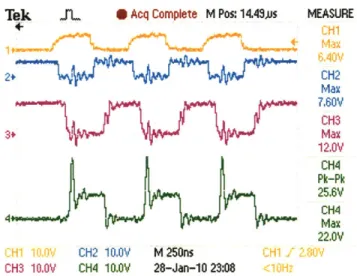
Unfortunately, modifying the board to include the inverter added more stray capacitance and therefore made the signals have more ringing and noise. This can be seen in Figure 23, where trace 1 (orange) is the input signal to the board (3 Mbps), trace 2 (blue) is the output of the inverter, trace 3 (purple) is the gate of the MOSFET, and trace 4 (green) is the drain of the MOSFET.
Tek JrL 0 Acq Complete M Pos: 14.43.us MEASURE
CH2 Max 7.60V CH3 3+ Max 12.0HJ CH4 Pk-Pk 25.6V? CH4 Max 22.0'? 11iT CH2 10,0'? M 250ns --C113 10.0'? CH4 10.0'? 28-Jan-10 23:08
Figure 23 Final transmitter testing with inverter added to the PCB
In future revisions, including the inverter as a surface mount component will greatly improve the signal. Additionally, it would be good to include test points to easily monitor the system, a key learning that was implemented with great success in the receiver printed circuit board.
I ohm 1 Ohm 1kain 3.5 Watt 3.5 att I Ohm 1 Ohm 3.5 Watt 3.Watt F9+ LED * ***..*
E3e E30 00000000 0 eeeee 0 4
*~ **9*009000 0 0 4 +24V 0000000000 0 0 4 0*000000 0 0 4 *0000*00* 0 0 4 - *0000 0 0 4 W GND GtID Opticl Trnswiter Hea~ sv adag.
MIT Sea Grant
July eam eeseeeee 0eeeeee9 00000000 00000000 00000000 00000000 00000000 00000000 Signal In cm TTL
r*
CTXD+su
Derd an RT'S Signal Out e. 0 eE3 I. 0 le .EV E3 0 +e2Figure 24 Transmitter PCB mechanical layout
Figure 25 Populated transmitter printed circuit board .... .. ...
3.2 Optical Receiver
The optical receiver system detects the optical signal and transforms it into an electrical signal. It consists of a photon detector, which converts an optical signal into an electrical current, as well as additional electronics to convert the photon detector's electrical signal into TTL voltage levels. Figure 26 shows this the system-level receiver design.
Amplification
Photon
--
+and
Data
Detector adDt
Processing
Figure 26 Receiver system diagram
Like the optical transmitter, the optical component of the receiver (in this case, the photon detector) determines the design of the rest of the system, which solely exists to condition the optical components output into a usable electrical form. Accordingly, the photon detector must be selected before the rest of the receiver design can continue.
3.2.1 Photon Detector
There are many different types of opto-electrical devices that can be used as photodetectors. Ideally, a photodetector would be able to quickly respond to all incident photons sent by the transmitter without introducing additional noise. Additionally, it would be small, robust, cheap, and power efficient. Unfortunately, many of these qualities are mutually exclusive and trade-offs must be made. In our application, switching speed is the top priority for a photon detector, followed by light sensitivity. Of course, this is assuming that power and size constraints are met. In the following sections, I will discuss different possible photon detectors and their strengths and weakness as they relate to an optical communications receiver.
3.2.1.1 Photoresistors
Photoresistors (see symbol in Figure 27), also known as light dependent Figure 27 resistors or cadmium sulfide (CdS) cells, are a type of photoconductor, Photoresistor meaning that their conductivity changes when exposed to electromagnetic symbol
radiation such as visible light(32). Photoresistors have a very high resistance, which can measure in the mega ohms (they are not conductive), when they are in the dark. When exposed to light, their resistance decreases linearly (over small regions) and may be as low as only a couple hundred ohms (19). Though they have very good light sensitivity, they respond very slowly. It typically takes over a millisecond for a photoresistor to fully respond to the presence of light. Additionally, it can take a couple of seconds for the photoresistor to return to its dark resistance after the light signal has ended. This is unacceptably slow for switching speeds of over 1 MHz.
3.2.1.2 Photothyristors
Photothyristors are another type of photodetector. They are just photo-activated thyristors, which are modified diodes. Like diodes, thyristors conduct current when their anode has a higher voltage than their cathode. But unlike diodes, thyristors have a third lead (the gate) that controls whether the
thyristor starts conducting current. The gate must have a positive voltage and Figure 28 sufficient current before the thyristor will turn on (33). After the thyristor is Photothyristor activated, the gate does not affect the thyristor anymore. This means that once symbol a photothyristor has been optically triggered, turning off the light will not turn
off the thyristor - only turning off power to the circuit or making the cathode have a positive voltage compared to the anode will do that. For this reason, photothyristors are not ideal for optical communication purposes.
3.2.1.3 Phototransistors
Phototransistors (see symbol in Figure 29) are like regular bipolar transistors or FETs, only their base (bipolar transistors) or gate (FETs) is exposed to light. When the photons hit the base or gate, either a current (bipolar transistors) or a voltage (FETs) is produced which starts to turn "on" the transistor (19). This means that when the phototransistor is in the dark, very little current flows through the transistor, but in the presence of light, the current or voltage signal produced by the light is amplified by the
Figure 29 Phototransistor
transistor's current gain as the transistor turns on and allows current to flow from the collector to the emitter. This internal gain (from one hundred to several thousand) makes phototransistors incredibly sensitive to any light signal (34). Unfortunately, they are only moderately fast (250 KHz) even though they are relatively robust with regards to noise (35).
3.2.1.4 Photomultipliers
Photomultiplier tubes (PMTs) are a type of vacuum tube that is very light sensitive (see Figure 30). Incident light produces electrons, which are accelerated and multiplied by dynode plates. The current can be multiplied over a million times after going through multiple dynode stages (34). Photomultiplier tubes are great for detecting low light level signals, as they are able to detect even single photons. Because of their high sensitivity, they are easily affected by ambient light. In order to produce such high gains, photomultipliers are large and need high voltage levels (thousands of volts) (36). They are fragile, easily affected
by magnetic fields, and expensive. Even though they can have a
response time of less than a nanosecond (37), their size, power consumption and fragility make them a poor choice for underwater optical communication.
Figure 30 Picture of a
photomultiplier (20)
3.2.1.5 p-n Photodiodes
Like the previous photon detectors, photodiodes convert light energy into electrical current. When incident light hits the photodiode, it turns the photodiode into a current source that pumps current from the cathode to the anode (19).
Anode Cathode
Photodiodes consist of n- and p-type semiconductors sandwiched together. The p-type has a surplus of holes and the n-type has excess electrons. Where the two types meet, the depletion region, holes and electrons recombine in order to equalize the number of free carriers in the semiconductor. This produces a positive net charge in the n-type material and a negative charge