HAL Id: tel-03139871
https://tel.archives-ouvertes.fr/tel-03139871
Submitted on 12 Feb 2021HAL is a multi-disciplinary open access
archive for the deposit and dissemination of sci-entific research documents, whether they are pub-lished or not. The documents may come from teaching and research institutions in France or abroad, or from public or private research centers.
L’archive ouverte pluridisciplinaire HAL, est destinée au dépôt et à la diffusion de documents scientifiques de niveau recherche, publiés ou non, émanant des établissements d’enseignement et de recherche français ou étrangers, des laboratoires publics ou privés.
model nanocatalysts for environmentally friendly energy
generation sources
Hang Liu
To cite this version:
Hang Liu. In situ investigations of chemical reactions on ZnO-Pt model nanocatalysts for environmen-tally friendly energy generation sources. Catalysis. Sorbonne Université; Northwestern Polytechnical University (Chine), 2019. English. �NNT : 2019SORUS201�. �tel-03139871�
Sorbonne Université
L'ECOLE DOCTORALE DE CHIMIE PHYSIQUE ET DE CHIMIE ANALYTIQUE DE PARIS CENTRE (ED 388)
In Situ Investigations of Chemical Reactions on ZnO-Pt
Model Nanocatalysts for Environmentally Friendly
Energy Generation Sources
Par
HANG LIU
Thèse de doctorat
Présentée et soutenue publiquement le 29/06/2019 Devant un jury composé de :
M. Philippe Jonnard Directreur de recherche Sorbonne Université (Président du jury)
M. Yanfeng Chen Professeur Nanjing University (Rapporteur) M. Xiaohua Ma Professeur Xidian University (Rapporteur) Mme. Lingyan Xu Maître de conférences Northwestern Polytechnical University (Examinatrice) M. François Rochet Professeur Sorbonne Université (Directeur de thèse) M. Wanqi Jie Professeur Northwestern Polytechnical
University (Co-directeur de thèse) M. Ahmed Naitabdi Maître de conférences Sorbonne Université (Co-encadrant,
1
Acknowledgements
First, I would like to thank Prof. Alain Dubois and my supervisor Prof. Wanqi Jie for providing me the opportunity to work in between the two laboratories, i.e. Laboratoire de Chimie Physique-Matière et Rayonnement in Sorbonne Université and the state key laboratory of solidification processing in Northwestern Polytechnical University.
Besides, I would like to thank my supervisor Prof. François Rochet for his insightful views, which incented me to widen my research during the three years. With his careful guidance, I overcame many difficulties of this project and learned a lot from him.
Also, I would like to thank my supervisor Prof. Ahmed Naitabdi for initiating and directing this project. I also appreciate his assistance, patient guidance and insightful views throughout this project. With his earnest instructions, I got over a lot of difficulties and made great progress in the process of the experiments.
Then I would like to thank all my colleagues in the lab (Alter Zakhtser, Anthony Boucly, Rabah Benbalagh, Régis Vacheresse and the others) for their help throughout these three years. Particularly, I give many thanks to Alter Zakhtser for his valuable contribution to this project and for sharing the happiness and sadness with me in these three years.
Finally, I would like to give many thanks to my parents, my father Tao Liu and my mother Yali Liu, who have been always supporting and understanding me unconditionally.
Special thanks to my girlfriend, Yuantao Liao, for standing by me during the ups and downs in these three years.
Paris, April 2019
2
Abstract
The inverse ZnO/Pt(111) catalyst has been shown to exhibit remarkable catalytic performances in the low temperature CO oxidation and represent a promising stable catalytic system. The identification of the active sites in CO oxidation is important for a mechanistic understanding of the structure-reactivity relationship. To reveal their nature, the catalytic role of the ZnO thin films on Pt(111) in the low-temperature CO oxidation was studied by UHV scanning tunneling microscopy (STM), low-energy electron diffraction (LEED) and near ambient pressure X-ray photoemission (NAP-XPS) in operando conditions. We have first established a reproducible recipe to fabricate well-ordered ZnO thin films on Pt(111) using e-beam evaporation process, followed by the structural characterizations of the thin films as a function of film thickness by STM and LEED. The film grows in layer-by-layer mode along the (0001) orientation, starting from a graphene-like monolayer to reaching the ZnO(0001)-Zn terminated bulk surface. From the structural evolution of ZnO thin films after exposure to 1 mbar of the O2: CO mixture (4:1), the special role of the ZnO/Pt boundaries was revealed. To shed more light on the role of the boundaries, a systematic comparative study of the ZnO/Pt(111) inverse catalyst with the plain Pt(111) surface was undertaken. The combined “embedded” mass spectroscopy and gas phase NAP-XPS analysis were relevant, first, to determine the regimes where mass transfer limitation starts to occur, allowing a sound discussion on the relation between steady-state molar fractions of reactants/product and surface reactivity, and, second, to calibrate the surface density of the adsorbates. Solid phase NAP-XPS spectra gave us access to the dynamics of the ZnO monolayer film covering only partially the Pt(111) single crystal surface. The pivotal, albeit unexpected role of ZnO-bound hydroxyls was clearly highlighted by the observation of the chemical signature of the CO+OH associative reaction products by XPS. The carboxyl formed at the low temperature (410 K) can be the intermediate species that leads to the evolution of CO2, the OHs at the Pt/ZnO boundary being the co-catalyst, which explains the synergistic effect of ZnO and Pt, we and others have observed. However, the species formed at the higher temperature (from 445 K) is a formate, that would essentially be a spectator.
3
Abbreviations
HOR: hydrogen oxidation reaction ORR: oxygen reduction reaction
NC-AFM: Noncontact atomic force microscopy SXRD: surface x-ray diffraction
PLD: pulsed laser deposition ML: monolayer
DFT: density functional theory TMO: transition metal oxide CUS: coordinatively unsaturated MLE: monolayer equivalent
STM: scanning tunneling microscopy UHV: ultrahigh vacuum
LEED: low energy electron diffraction STS: scanning tunneling spectroscopy XPS: X-ray photoelectron spectroscopy
NAP-XPS: near-ambient pressure X-ray photoelectron spectroscopy LDOS: local density of states
HOMO: highest occupied molecular orbital LUMO: lowest unoccupied molecular orbital BE: binding energy
KE: kinetic energy
QMS: quadrupole mass spectrometer Fcc: face-centered cubic
MTL: mass transfer limitation
IRAS: infrared reflective absorption spectroscopy h-BN: hexagonal boron nitride
XRD: X-ray diffraction
FT-IR: fourier transform infrared spectrometer UV-Vis: ultraviolet-visible spectrophotometer THz: terahertz
4
Contents
Acknowledgements ...1 Abstract ...2 Abbreviations ...3 Contents ...4 Chapter 1: Introduction ...61.1 Concerns of the environmental issues ...6
1.2 Hydrogen fuel cells ...7
1.3 Inverse oxide/metal catalysts ...8
1.4 Zinc oxide structures ... 11
Polar surface structures of the ZnO crystal ... 12
Structures of ultrathin ZnO films ... 14
1.5 CO oxidation on the inverse ZnO/Pt(111) catalyst ... 20
Chapter 2: Experimental setup ... 23
2.1 Electron beam evaporation (e-beam evaporation) ... 23
2.2 Scanning tunneling microscopy (STM)... 24
Theory of scanning tunneling microscopy ... 24
Description of scanning tunneling microscopy ... 27
Fabrication and cleaning of the tip for scanning tunneling microscopy... 29
2.3 Scanning tunneling spectroscopy (STS) ... 30
2.4 Low-energy electron diffraction (LEED) ... 32
Description of low-energy electron diffraction ... 32
Theory of low-energy electron diffraction ... 33
Surface structures ... 34
2.5 Near-ambient pressure X-ray photoelectron spectroscopy (NAP-XPS) ... 35
Principle of X-ray photoelectron spectroscopy ... 35
Description of X-ray photoelectron spectroscopy ... 38
Description of near-ambient pressure X-ray photoelectron spectroscopy ... 39
2.6 Quadrupole mass spectrometer (QMS) ... 43
Chapter 3: Fabrication of ZnO thin films on Pt(111) ... 45
3.1 Preparation of the Pt(111) substrate ... 45
3.2 Preparation of ZnO films on Pt(111) ... 46
5
3.4 Summary and conclusions ... 51
Chapter 4: Morphology evolution of ZnO films on Pt(111) under CO oxidation conditions .. 53
Summary and conclusions ... 58
Chapter 5: CO oxidation mechanisms at the ZnO/Pt(111) model catalyst ... 59
5.1 NAP-XPS setup as a flow reactor ... 59
5.2 QMS molar fractions for the plain Pt(111) and the ZnO/Pt(111) surfaces ... 60
5.3 CO oxidation reaction on the plain Pt(111) surface ... 63
5.4 CO oxidation reaction on the ZnO/Pt(111) surface ... 68
5.5 Carboxyl/formate species, reaction intermediates or spectators? ... 76
5.6 Summary and conclusions ... 81
Chapter 6: Conclusion and perspectives ... 83
6.1 Conclusions ... 83
6.2 Perspectives ... 85
Appendix: Synthesis of the large-diameter ZnTe crystal for THz emitting and detection ... 86
Introduction ... 86
Experimental setup ... 87
Results and discussion ... 88
Conclusions ... 93
6
Chapter 1: Introduction
1.1 Concerns of the environmental issues
The rapid development of the economy has brought about the increasing pace of the energy consumption throughout the world. For more than 30 years, the petroleum and coal have dominated most of the world energy consumption (Figure 1.1), which are satisfying the population’s need. However, the resulting emission from the combustion of the fossil fuel has become the main cause of the air pollution, which leads to a negative impact on the environment and people [1].
Figure 1.1: World energy consumption by energy source (1990-2040). Source: U.S. Energy Information Administration, International Energy Outlook 2017.
There are several key air pollutants arising from the combustion of the fossil fuels, such as sulfur oxides (SOx), nitrogen oxides (NOx), particulate matter (PM) and carbon monoxide (CO). These pollutants are mainly related to the human activity particularly due to transportations and household (Figure 1.2). These emissions are eventually causing the premature death of humans (e.g. heart disease and lung cancer), climate changes (warming and cooling effect) and acidification of water, etc. Nowadays due to the growing attention to air pollution, governments from all over the world are devoted to tackle this serious problem. Several regions in the world, such as Europe, and other major countries especially China are taking strong and leading actions not only in environmental remediation measures but also and most importantly in innovative solutions to provide energy with low environment impact. Based on more and more efforts and international collaborations, to 2040, the total global emission of
7 air pollutants will be controlled on a declining trend with applications of air-pollution control technologies and the transition to the cleaner energy [1].
Figure 1.2: Primary air pollutants and their sources [1].
1.2 Hydrogen fuel cells
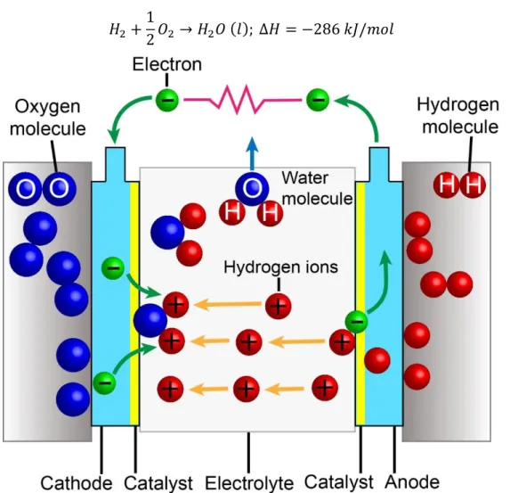
Hydrogen is an attractive synthetic fuel which can be used in fuel cells that are potential alternatives to the combustion and fossil fuel based energy generators They can be used especially for transportation and electricity generation [2] which are considered major energy sectors. Hydrogen fuel cell is a very promising technology which can convert hydrogen and oxygen efficiently into electricity at a relatively low operating temperature. There are a variety of different types of fuel cells which are classified either by the electrolyte employed or by the operating temperature [3]. Figure 1.3 gives an example of a fuel cell, which is the polymer electrolyte membrane fuel cell (PEMFC). PEMFC is a low-temperature fuel cell (the operating temperature 60-120 ℃), in which the two electrodes are separated by a proton exchange membrane (an electrolyte) [3, 4]. The basic working principle can be described as three steps:
In the first step, hydrogen is introduced to the anode of the fuel cell and then hydrogen molecules split into hydrogen atoms;
In the second step, the hydrogen oxidation reaction (HOR) takes place with a catalyst lining the anode. Then the protons (H+) can go through the polymer electrolyte membrane,
8 reaching the cathode. Meanwhile, the electrons travel through an external circuit to arrive at the cathode, creating a current. The HOR equation is expressed as:
𝐻2 → 2𝐻++ 2𝑒− (1)
In the third step, oxygen at the cathode reacts with the protons and electrons from the anode, forming water as the only side product. This reaction is the oxygen reduction reaction (ORR), which is described as:
1
2𝑂2+ 2𝐻
++ 2𝑒− → 𝐻
2𝑂 (2)
Hence, the overall reaction of PEMFC can be written as: 𝐻2+
1
2𝑂2 → 𝐻2𝑂 (𝑙); ∆𝐻 = −286 𝑘𝐽/𝑚𝑜𝑙 (3)
Figure 1.3: Schematic of a hydrogen fuel cell.
1.3 Inverse oxide/metal catalysts
The fundamental science and industrial technologies such as the energy conversion and the pollution control emphasize the crucial role of Pt-based materials as one of the prominent catalysts [3, 5, 6]. In fact, platinum, one of the most important transition metals, is widely used
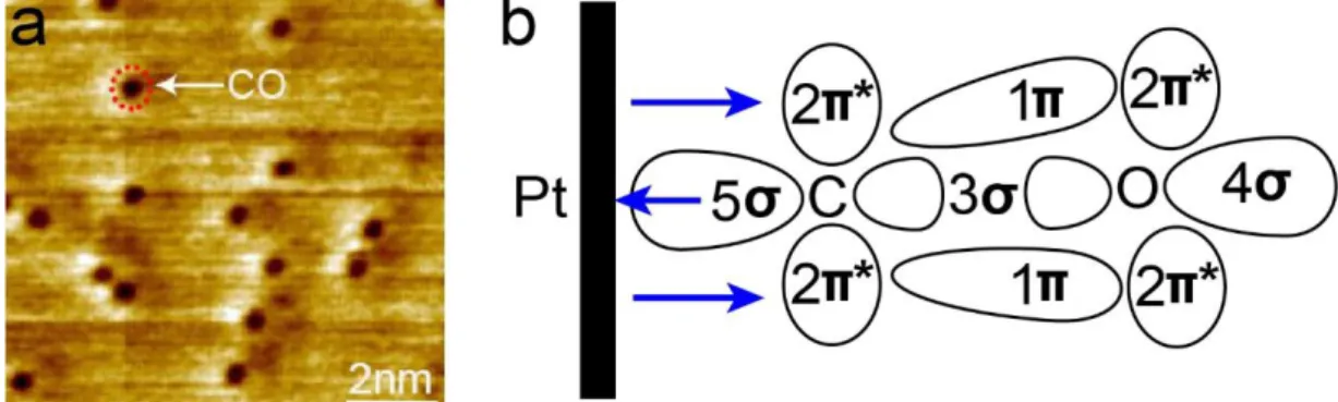
9 in heterogeneous catalysis due to its high activity and selectivity for many chemical reactions [7-9], such as CO oxidation [10] and CO2 hydrogenation [11]. Nevertheless, Pt mainly suffers from two severe issues, which are CO poisoning resulting in a rapid deactivation and material dissolution, respectively [12, 13]. CO strongly adsorbs on the Pt surface, which blocks the active sites and deactivates the catalytic reaction on the surface. For instance, in a hydrogen fuel cell, CO, which is the contamination in H2 gas, adsorbs on Pt catalysts and tremendously decreases the kinetics of the HOR and ORR at anode and cathode [3]. Figure 1.4(a) shows that CO molecules were observed as the dark protrusions on the Pt(111) surface at room temperature in a base pressure of 10-10 mbar. The strong adsorption of CO on the Pt surface is generally described by the Bolyholder model (Figure1.4(b)) [14], in which electrons are donated from CO via a σ bond to the d-band of Pt and meanwhile electron back-donation process takes place via transferring electrons from Pt to the 2π* orbital of CO.
Figure 1.4: (a) Our STM image of Pt(111) surface (tunneling condition: 0.2 V, 500 pA); (b) Schematic of the Bolyholder model.
On the other hand, Pt is a scarce and expensive metal as shown in Figure 1.5, which limits the widespread practical applications in industry. Recently, new research efforts have been emerging in order to address the limitations (CO poisoning, material dissolution and high price of Pt) and produce catalysts with enhanced stability [15, 16]. In particular, the transition metal-oxide nanocatalysts are of paramount interest in the development of efficient catalytic materials, which provides a suitable method to partially replace Pt by a more abundant transition metal [16-18]. Thus the decrease of Pt-load in the catalysts is currently attracting large attention as a suitable method to decrease the high cost of catalysts. Indeed, recently, Zn has emerged as one of the most promising elements in bimetallic catalysts owing in part to the stability of its oxide (ZnO) under reducing conditions [16, 18-20] and its greater affinity with oxygen compared with that of Pt. Elligham diagrams show Zn is thermodynamically able to reduce PtO2 to Pt, forming ZnO. Hence, Zn, an affordable metallic material (see Figure 1.5), could
10 offer a good opportunity to form an efficient catalyst when it combines with Pt. Indeed, ZnO/Pt is active for CO oxidation [19] and promotes catalytic reactions related to fuel cells [20, 21].
Figure1.5: Price of the elements ($/kg) versus their annual production (kg/yr) [22]. The classic heterogenous catalysts consist of metal particles dispersed over an oxide support, which is called conventional metal/oxide catalysts (Figure 1.6) [23]. In this system, metal nanoparticles suffer premature deactivation and decomposition, due several effects: (i) the encapsulation of the metallic catalysts by the support, (ii) the decomposition and corrosion of the support under operating conditions [24]. Besides, the oxide support is either considered as a simple template for the metal dispersion or it can directly participate in the catalytic process [17]. However, in recent years there is a motivation to improve the configuration of the conventional catalyst by taking advantage of the intrinsic properties of metal oxide. Indeed, oxide nanoparticles has presented special physical and chemical properties due to their size, a high density of defects and corner or edge sites on their surface [25]. The concept of the inverse oxide/metal catalyst was defined by Rodriguez and his coworkers [17, 26], which means nanoparticles of a metal-oxide are deposited on a metal surface (Figure 1.6). Another advantage of this system consists of the stability of metallic surfaces and the strong thermodynamic stability of thin film of metal-oxides. The study of inverse oxide/metal nanocatalysts offers great promises in the understanding of the role of oxide and oxide-metal interface in a catalytic process. Furthermore, the strong metal-oxide interaction of the inverse oxide-metal catalyst can have an effect on the electronic states of oxide nanoparticles, which produces new chemical properties [17]. In our work, the inverse ZnO/Pt(111) catalyst is studied to understand the
11 relationship between the chemical structure and the reactivity of ZnO nanostructures supported on Pt(111) single crystal relevant for CO oxidation reaction.
Figure1.6: Schematics of a conventional metal/oxide and an inverse oxide/metal catalyst.
1.4 Zinc oxide structures
Zinc oxide (ZnO) is an n-type semiconductor with a direct bandgap of ~3.3 eV at 300 K [27]. At the ambient pressure and room temperature, the thermodynamically stable structure of ZnO is wurtzite, (as shown in Figure 1.7 (a)), where each cation is surrounded by four anions at the corners of a tetrahedron, and vice versa [28]. The tetrahedral coordination typically represents sp3 covalent bonding, however ZnO shows a relative strong ionic character. Therefore, ZnO, as a Ⅱ-Ⅵ compound, shows the ionicity between an ionic behavior and a covalent behavior. ZnO has a hexagonal unit cell with two lattice parameters, 𝑎 = 3.2495 Å and 𝑐 = 5.2069 Å . In this type of structure, there are four common low-index surfaces: the non-polar (101̅0) and (112̅0) surfaces, and the polar (0001)-Zn and (0001̅)-O surfaces [29]. The polar surfaces are formed either by Zn or O ions, while the non-polar surfaces exhibit an equal number of Zn and O ions [30]. Apart from the wurtzite structure of ZnO, the zinc-blende structure can also be obtained by growth on the cubic substrate (as seen in Figure 1.7 (b)) [28], and the rocksalt structure is possibly stable at a relative high pressure (~10 GPa) (Figure 1.7 (c)) [31].
Figure1.7: Unit cells of ZnO crystals: (a) Wurtzite structure; (b) Zinc blende structure; (c) Rock salt structure. Zinc and oxygen atoms are yellow and white, respectively.
12 Polar surface structures of the ZnO crystal
Compared with the non-polar surfaces ((101̅0) and (112̅0)), the polar surfaces of ZnO ((0001)-Zn and (0001̅)-O surfaces) are more interesting from the scientific and technological points of view [32]. The hexagonal wurtzite structure of ZnO is represented as alternating planes made up of fourfold-coordinated Zn2+ and O2- ions along the c axis with alternating distances 1.99 Å and 0.69 Å, respectively [33]. Therefore, a (0001)-Zn terminated surface or a (0001̅)-O terminated surface is created by cutting the ZnO crystal perpendicular to the c axis. If these two ZnO polar surfaces are not compensated, the electrostatic potential increases due to the divergence of the net diploe moment when increasing the thickness of ZnO crystal [32-34], as shown in Figure 1.8. In order to reduce the electrostatic energy, three surface stabilization mechanisms are generally put forward [33]: (1) reduction of the charges of the Zn (O) surface by adsorption foreign molecules; (2) surface reconstruction by removal of surface atoms; (3) transfer of negative charge from the O plane to the Zn plane and creation of new surface states.
Figure1.8: Schematics of (a) the charged planes with the dipole moment normal to the surface and (b) the thickness versus the electrostatic potential [35].
The current work on (0001)-Zn terminated surface of the ZnO crystal by Dulub and coworkers [33, 36] shows that this polar surface is stabilized by the formation of triangular islands and pits, as shown in Figure 1.9 (a). Many triangular islands and pits are observed on the surface with a step height of ~ 2.7 Å, which corresponds to a single layer (half of the unit cell). Besides, the inner holes of the triangular islands are also found, whose orientation and shape depends on the size of the islands. Density functional theory (DFT) calculations (Figure 1.9 (b)-(d)) implies a 0.25 occupancy of Zn ions is deficient on the surface, and step edges of islands and holes are terminated by under-coordinated O atoms, which agrees with the
13 stabilization mechanism (2). In addition, this mechanism is suggested to be stable over a wide range of oxygen and chemical potentials [36].
Figure1.9: (a) STM images of the (0001)-Zn terminated surface; (b)-(d) DFT calculated ZnO islands with different sizes [33].
The morphology of the (0001̅)-O terminated surface is different compared to that of the (0001)-Zn terminated surface, as shown in Figure 1.10 (a). The hexagonal terraces are observed with mainly a double step height of ~ 5.4 Å, which are typically terminated by step edges including an angle of 120˚ [30]. DFT calculations illustrate that the double-height step edges are stoichiometric, which consist of O-terminated (1̅010) and Zn-terminated (001̅0) edges [30].
Figure1.10: (a) STM image of the (0001̅)-O terminated surface; (b) and (c) are the top-view and side-view models of hexagonal terraces, respectively [30].
14 Unlike the (0001)-Zn terminated surface which is stabilized by triangular islands and holes, the (0001̅)-O terminated surface is found to be stabilized by adding a half-monolayer hydrogen (H) which leads to the formation of terminal hydroxyls (OH) on the unreconstructed (1×1) ZnO surface at room temperature (shown in the noncontact atomic force microscopy (NC-AFM) image in Figure 1.11 (a)). This provides the stabilization mechanism of the surface (1) [37]. Moreover, the XPS measurement of the O 1s photoemission spectra confirms OH species on the surface, which has a shifted binding energy peak ( at 532.3 eV) compared to the main peak (530.4 eV) which corresponds to the O 1s of the lattice, as shown in Figure 1.11 (b) [37]. In fact, the hydroxyls would disappear from the surface when heating the ZnO sample to 450 ℃ [37]. The H source of OH groups formed on the (0001̅)-O surface might come from the ambient environment (such as H2O and H2) and bulk H (interstitial H atoms present in bulk of the crystal) [29, 38], which cannot be ignored even under excellent UHV conditions. Residual water molecules are ubiquitous in the UHV. Moreover, DFT calculations corroborate that the hydrogenated surface is the most stable one over a wide range of pressures and temperatures [39].
Figure1.11: (a) High-resolution, constant height NC-AFM image (50 × 80 Ǻ, VCP = 4.3 V, Δfset = -111 Hz) of the H-covered surface ZnO(0001̅) in the (1×2) H-covered state at room temperature; (b) O1s XPS spectra of the ZnO(0001̅) surface. [37]
Structures of ultrathin ZnO films
For the ultrathin ZnO film with a thickness of only a few atomic layers, a new stabilization mechanism becomes effective, which is due to the stabilizing role of the support
15 and/or due to the ability of finite systems sustaining a nonzero polarization along the polar axis [34].
The first DFT calculations on the new phase of the ZnO film were reported by Claeyssens and coworkers [40, 41], who were investigating the deposition of thin ZnO films as templates for aligned growth of ZnO nanorods. When considering ZnO thin films (less than 18 layers) terminating with the polar (0001) and (0001̅) surfaces, the energy of the flattened ZnO structure is much lower than that of the wurtzite ZnO structure. In this configuration, each Zn atom is bonded with three O atoms instead of four O atoms in the bulk, and vice versa, resulting in a co-planar structure composed of flat Zn3O3 hexagonal rings. In fact, this new ZnO structure is the same as the graphene or the hexagonal boron nitride (h-BN) structure. The transition between the wurtzite structure and graphene-like structure is shown in Figure 1.12.
Figure1.12: (a) Model of the polar wurtzite structure of a ZnO film; (b) Model of a graphitic structure of a ZnO film. Zn atoms are in light blue and O atoms are in red. [40, 41]
Afterwards, the experimental existence of the h-BN ZnO structure was observed by Tusche and colleagues [42], who were studying ZnO films grown on Ag(111) using scanning tunneling microscopy (STM) and surface X-ray diffraction (SXRD). ZnO was fabricated by pulsed laser deposition (PLD) at 300K using a stoichiometric ZnO target in a 5 × 10⁻⁷ mbar of O2, followed by annealing up to 680K. The coverage of the ZnO film was examined from 2.2 to 4.5 monolayers (ML) by STM measurements. Figure 1.13 (a) shows a STM image of a 2.2 ML ZnO film, which is characterized by an atomically flat ZnO double-layer decorated with some triangular islands on the third layer. Besides, the high resolution STM image of the 2.2 ML film, in Figure 1.13 (b), shows a distinct Moiré pattern corresponding to the coincidence lattice of 7 ZnO to 8 Ag(111) atoms, which is an indicator of the successful synthesis of the h-BN ZnO films on Ag(111). Back to Figure 1.13 (a), the inset shows the STM image of a 3.2
16 ML ZnO film on the same lateral scale as Figure 1.13 (a). Compared to the 2.2 ML ZnO film, the surface of the 3.2 ML ZnO film is rougher with incomplete layers forming small islands. The further SXRD illustrates the transition from the h-BN to the bulk wurtzite structure occurs around 3-4 ML coverage, which is connected to the surface roughness of the ZnO film, as shown in Figure 1.13 (c) and (d). Surprisingly, this transitional thickness to the bulk wurtzite is much smaller than the thickness calculated by Claeyssens and coworkers [40, 41], as mentioned above.
Figure1.13: (a) STM image of 2.2 ML ZnO on Ag(111). The inset is 3.2 ML on the same sale; (b) High resolution STM image of 2.2 ML film; (c) Distance (dnm) between layer number n and m; (d) Oxygen coordinate (un) in layer number n; (e) Schematic of the bulk ZnO (wurtzite) structure; (f) Schematic of h-BN ZnO structure. [42]
An important study was reported by Deng and coworkers [43], who were using the reactive deposition of e-beam evaporated pure Zn under NO2 at a pressure of 3 × 10⁻⁸ mbar at room temperature. The use of NO2 instead of O2 was mentioned because they discovered Zn was unable to fully oxidized with O2 up to 2 × 10⁻⁶ mbar. The ZnO film on Au(111) presents two types of nanostructure, both of which display a Moiré pattern with a periodicity of ~ 23 Å
17 forming a ZnO(0001)-(7 ×7)/ Au(111)-(8 × 8) supercell. The two types of structures are defined by different heights, ~ 3.5 Å indicating single-layer ZnO and ~ 5.5 Å referring to bilayer ZnO, as seen in Figure 1.14 (e) and (f) (the STM height is not comparable to the physical height due to the electronic contributions involved in the STM measurements). Both the single and bilayer ZnO adopt a planar, graphene-like structure. When increasing the temperature from room temperature to 550K, the bilayer ZnO gradually becomes the dominant species on Au(111) instead of single-layer ZnO, as shown in Figure 1.14 (a-d). DFT calculations explain the interaction between ZnO layers are twice stronger than adhesion of ZnO with Au substrate, and therefore the bilayer is energetically favored with increasing the temperature.
Figure 1.14: STM images (100 nm× 100 nm) of 0.9 ML ZnO on Au(111) using the reactive deposition followed by annealing at 550 K for (a) 5; (b) 30; (c) 60; and (d) 120 min; (e) and (f) are the Line scans specified in (a) and (d); (g) and (h) are the side views of the optimized structures of the single and bilayer ZnO(0001) on Au(111), respectively. [43]
Another study of ZnO on Au(111) focused on the transition from the graphene-like structure to the bulk wurtzite structure, as shown in Figure 1.15. Using STM and DFT calculations, the transition is found to occur around four layers of ZnO [44], which is in agreement with the aforementioned ZnO/Ag(111) system.
18 Figure 1.15: (a) STM image of a ZnO structure on Au(111) using reactive deposition method at 465 K; (b) Height profile along the solid green line in (a). [44]
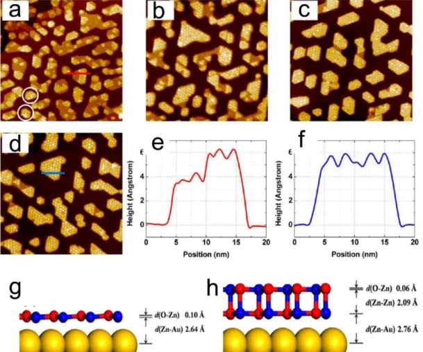
As for ZnO deposited on Pd(111), a significant study was reported by Weirum and coworkers [34], who deposited Zn under 5 × 10⁻⁷ mbar O
2 at room temperature, followed by annealing in O2 at 550 K. In the sub-monolayer range, two competing structures were observed, one is a honeycomb-like (4 × 4) phase, the other is a compact, graphene-like (6 × 6) phase, as shown in the STM images in Figure 1.16 (a) and (d), respectively. The (4 × 4) phase exhibits a honeycomb-like hexagonal unit cell (indicated in Figure 1.16 (a)) with a length of 11 Å, which corresponds to 4 times the lattice constant of the Pd(111) surface, in agreement with the p(4 × 4) LEED pattern in Figure 1.16 (b). The further DFT analysis confirms this structure has a Zn6OH5 stoichiometry, as shown in Figure 1.16 (c). The (6 × 6) phase shows a hexagonal structure with a lattice constant of 3.2 Å (indicated with a small rhomb in Figure 1.16 (d)), which is aligned with the in-plane lattice parameter (3.25 Å) of the ZnO(0001) surface. Moreover, a Moiré pattern with a periodicity of 16.5 Å is visible in Figure 1.16 (d), which corresponds to 6 times the Pd lattice constant or 5 time the ZnO lattice constant. This coincident lattice is reflected in the corresponding LEED pattern in Figure (e), which shows the Pd diffraction spots are surrounded by satellite spots. The subsequent DFT calculation suggests this compact phase has a Zn6O6 stoichiometry, as shown in Figure 1.16 (f).
19 Figure 1.16: (a) High-resolution STM image of the (4 × 4) phase (65 Å × 65 Å); (b) Corresponding (4 × 4) LEED pattern; (c) Structural model of (4 × 4) phase. Pd, O, Zn and H atoms are in gray, white, blue and red, respectively; (d) High-resolution STM image of the (6 × 6) phase (50 Å × 50 Å); (e) Corresponding (6 × 6) LEED pattern; (f) Structural model of (6 × 6) phase. Pd, O and Zn atoms are in gray, white and blue, respectively. [34]
Since Pd and Pt are the siblings in the nickel family, a further study of ZnO on Pt(111) was provided by Liu and colleagues [45], who prepared ZnO films by Zn deposition in 10-7 mbar of O2 at room temperature, followed by oxidation at 600 K in 10-6 mbar of O2 for 5 min in order to achieve better ordered films. In the sub-monolayer ZnO regime (as shown in Figure 1.17), the (6 × 6) ZnO phase could spontaneously transform into the (4 × 4) in UHV at room temperature after several hours, which would re-transform into the (6 × 6) phase after heating at 600 K under 10-6 mbar of O
2. In fact, the (4 × 4) ZnO phase observed on Pt(111) and Pd(111), must be attributed to a much higher affinity of these substrates towards hydrogen than Ag(111) and Au(111), since the (4 × 4) structure has not been obtained on Ag(111) and Au(111). In addition, the residual hydrogen (possibly from water) in UHV also may play a crucial role in the formation of hydroxyls on ZnO surfaces.
20 Figure 1.17: STM images and LEED patterns of the ZnO/Pt(111) surfaces at the sub-monolayer coverage: (a) as-prepared and (b) after a few hours at room temperature in UHV chamber. [45]
1.5 CO oxidation on the inverse ZnO/Pt(111) catalyst
Low temperature CO oxidation is considered as a prototype reaction on inverse oxide/Pt(111) catalysts, where 3d transition metal oxide (TMO) islands partly cover a platinum surface [46-48]. The attention of the researchers focused on the synergetic effect that could be observed at the platinum/TMO boundary [46, 48]. Indeed, the removal of pre-adsorbed CO by a steady-state flux of O2 (under a pressure in the 10-8 mbar range) was observed at room temperature, both for the FeO/Pt(111) system [46] and the NiO/Pt(111) system [47], which is naturally impossible on the pure Pt(111). It was shown that the reactivity of CO oxidation increases with the FeO1-x/Pt boundary length per surface unit [46], which supports the idea that the reaction takes place at the phase boundary. Further theoretical calculations addressing a series of 3d TMOs showed that the key reaction site is a coordinatively unsaturated (CUS) metal cation combined to nearby platinum atoms [48], as shown in Figure 1.18. Besides the TMO oxides (FeO and NiO) that were known experimentally to be efficient when combined with Pt(111), the theoretical calculations by Sun and coworkers [48], also explored the reactivity of a filled 3d band transition metal oxide ZnO. When compared to the pure Pt(111), the Pt-CUS Zn2+ ensemble favors the breaking of the O-O bond and lowers the barrier for CO oxidation by about 0.4 eV, according to calculations. Although the Pt-CUS Fe2+ ensemble presents a lower CO oxidation barrier than the Pt-CUS Zn2+ one, the single oxidation state of Zn (2+) is a tremendous advantage with respect to the former case, because the ferrous oxide can become ferric oxide under O2 rich conditions, which is highly detrimental to its efficiency [46]. Therefore, theoretical predictions make the ZnO/Pt(111) system worthy of interest, especially in oxygen-rich CO/O2 mixtures.
21 Figure 1.18: Schematic structure of the inverse TMO/Pt(111) system in top view (a) and side view (b). The supercell used is indicated by a white rectangle with in-plane x and y axes. The blue, red, and green spheres represent Pt, O, and 3d TMs atoms, respectively. [48]
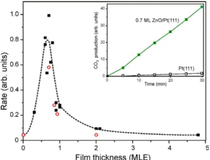
The first announcement of synergetic effect for a discontinuous sub-monolayer ZnO film supported by Pt(111) was made by Martynova and coworkers in 2013 [19]. Apparently, no experiment was carried out by the Berlin group at room temperature, where synergistic effects were already observed for the “benchmark” FeO/Pt(111) system [46]. However, at a temperature of 450 K and under an oxygen-rich O2: CO mixture (50 mbar: 10 mbar, He balance to 1 bar), the CO2 production rate measured at the outlet of the reaction chamber was found to be circa one order of magnitude higher on the films of the partial ZnO coverage than on the bare Pt(111), as shown in Figure 1.19. Indeed, at this temperature the pure Pt(111) surface may still be CO poisoned, as a technique like near-ambient pressure photoemission spectroscopy (NAP-XPS) indicates that in oxygen-rich mixtures the transition between CPt(111) to O-Pt(111) occurs in 515-535 K range, which was reported by Knudsen and coworkers [49]. Therefore, the activation of Pt-CUS Zn2+ sites can be effective at 450 K for CO oxidation.
Given the promises of the ZnO/Pt(111) system in low temperature CO oxidation, further studies need to be performed, focusing on several issues that were not addressed in the pioneering work of Martynova and coworkers [19]. First, instead of a single temperature (450 K), CO oxidation should be examined in a wide range of temperatures, from room temperature, where the added value of “inverse” catalysis is prominent due to the poisoning of Pt by CO, to the high temperature regime above ~ 520 K, where Pt itself is the most reactive [50] (the active phase is the O-covered metallic Pt(111) surface by Ertl and coworkers [51] when CO has desorbed from Pt areas). Second, information on the chemical species presented at the ZnO/Pt(111) surface should be collected when it is exposed to the O2: CO mixture, as the preceding work [19] was based on the gas composition measurements (at the chamber outlet) and the “post-mortem” STM observation of the surfaces. Another major aspect that has not
22 been addressed in previous studies concerns the identification of intermediate species in the CO oxidation reaction. Our study provides a better investigation in this regard and hence offers a clear understanding of the mechanism of the CO oxidation reaction.
Figure 1.19: CO2 production rate measured over ZnO films on Pt(111) as a function of the nominal film thickness (in MLE). The solid and open symbols show data for the films prepared using reactive Zn deposition at 85 and 300 K, respectively. The inset shows kinetic curves for CO2 production on the pure Pt(111) and 0.7 ML ZnO(0001) film. [19]
23
Chapter 2: Experimental setup
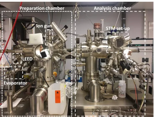
The experiments reported in the thesis were conducted in two independent ultrahigh vacuum (UHV) chambers, one related to the scanning tunneling microscopy (STM) measurements, and the other dedicated to the synchrotron near-ambient pressure X-ray photoelectron spectroscopy (XPS) measurements. Both UHV systems for STM and NAP-XPS measurements comprise two chambers, one is the preparation chamber equipped with the electron beam evaporator (e-beam evaporator), low-energy electron diffraction (LEED), and the facilities for crystal cleaning, and the other is the analysis chamber containing a STM microscope (a variable temperature XA microscope from Omicron NanoTechnology) or an NAP-XPS analysis setup.
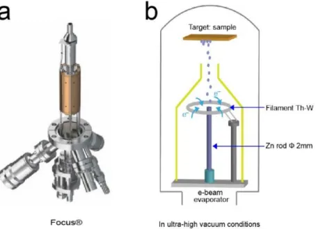
2.1 Electron beam evaporation (e-beam evaporation)
Zinc evaporation is performed using e-beam evaporation in UHV conditions method. Figure 2.1 shows the e-beam evaporator and the schematic of e-beam evaporation process, respectively. Zn wires (diameter = 2 mm, purity = 99.5%) are contained in a Mo crucible in the evaporator. When the evaporator works, the crucible is bombarded with electron beams from a tungsten filament controlled by a power supply. Consequently, Zn wires are heated in the crucible above the melting temperature (692.68 K). Zn atoms in the vapor phase precipitate and then form a thin film onto the Pt(111) single crystal.
24
2.2 Scanning tunneling microscopy (STM)
Scanning tunneling microscopy was invented by Gerd Binnig and Heinrich Rohrer [52-54] in 1982, who were awarded the 1986 Nobel physics prize in physics. STM has proven to be a powerful technique in surface nanoscience and nanotechnology over the past three decades, which provides access to investigate the surface topography with atomic resolution, the local density of states in samples ranging from metal, semiconductors to superconductors, and manipulate individual atoms and molecules on the sample surface.
Figure 2.2: The STM setup of Laboratoire de Chimie Physique - Matière et Rayonnement of Sorbonne Université in France.
Theory of scanning tunneling microscopy
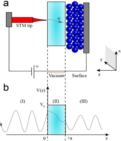
The concept of quantum tunneling effect plays an important role in the design and development of STM, as shown in Figure 2.3(a). In classical physics, an electron cannot penetrate or cross a barrier if its energy is smaller than the energy of the barrier. However, in quantum mechanics, an electron can tunnel through a barrier with some probability. Figure 2.3(b) shows the process of an electron crossing a potential barrier. For a rectangular barrier, the wave function of an electron in the direction z is described by the Schrodinger’s wave equation as:
25 (− ℏ
2
2𝑚∗∇2+ 𝑉(𝑧)) Ψ(𝑧) = 𝐸𝜓(𝑧) (4)
where ℏ is the reduced Planck constant, Ψ is the wave function of the electron, 𝑚∗ is the effective mass of the electron, ∇2 is the Laplacian, 𝐸 is the energy of the electron and 𝑉(𝑧) is
the potential energy. Particularly, the potential energy 𝑉(𝑧) varies with the position z, which causes the Schrodinger wave equation becomes a non-constant coefficient differential equation. Therefore, to solve this problem, the Schrodinger wave equation is separated in three regions where 𝑉(𝑧) is constant in each region, which are
Region (I): 𝑧 < 0, 𝑉 = 0 (5)
Region (II): 0 ≤ 𝑧 ≤ 𝑎, 𝑉 = 𝑉0 (6)
Region (III): 𝑧 > 𝑎, 𝑉 = 0 (7)
Consequently, the corresponding solution of the Schrodinger wave equation in each region is
Region (I): 𝜓(𝑧)I= 𝐴1𝑒𝑖𝑘𝑧+ 𝐴1′𝑒−𝑖𝑘𝑧 (8)
Region (II): 𝜓(𝑧)II = 𝐴2𝑒𝐾𝑧+ 𝐴′2𝑒−𝐾𝑧 (9) Region (III): 𝜓(𝑧)III= 𝐴3𝑒𝑖𝑘𝑧+ 𝐴
3
′𝑒−𝑖𝑘𝑧 (10)
where 𝐴1, 𝐴1′, 𝐴
2, 𝐴2′ and 𝐴3 are constants, 𝑘 = √ 2𝑚𝑒𝐸
ℏ2 and 𝐾 = √
2𝑚𝑒(𝑉0−𝐸)
ℏ2 . Since there is no
potential disturbance to reflect the wave in Region (Ⅲ), 𝐴3′ = 0.
By following the boundary conditions at 𝑧 = 0 and 𝑧 = 𝑎, which are
𝜓(0)I= 𝜓(0)II (11)
𝜓ꞌ(0)
I= 𝜓ꞌ(0)II (12)
𝜓(𝑎)II = 𝜓(𝑎)III (13)
𝜓ꞌ(𝑎)II = 𝜓ꞌ(𝑎)III (14)
The tunneling probability can be obtained as 𝑇 = |𝐴3
𝐴1|
2
= 4(𝑉0− 𝐸)𝐸
4(𝑉0− 𝐸) + 𝑉02𝑠𝑖𝑛2(𝐾𝑎) (15)
which is the squared modulus of the ratio between the probability density of the transmitted electrons and the probability density of the incident electrons. If 𝐾𝑎 ≫ 1, 𝑇 can be simplified as
26 𝑇 ≈16(𝑉0− 𝐸)𝐸
𝑉02 𝑒−2𝐾𝑎 (16)
which means the tunneling probability decreases exponentially with the width of the potential barrier.
The electron tunneling can also be described by the Bardeen’s model [55], which uses time dependent perturbation theory. Using Fermi’s golden rule, the tunneling current between the tip and sample is expressed as:
𝐼 =4𝜋𝑒 ℏ ∫ [𝑓(𝐸𝐹− 𝑒𝑉 + 𝐸) − 𝑓(𝐸𝐹+ 𝐸)]𝜌𝑇(𝐸𝐹− 𝑒𝑉 + 𝐸)𝜌𝑆(𝐸𝐹 + 𝐸)|𝑀𝑇𝑆| 2𝑑𝐸 +∞ −∞ (17) where 𝑓(𝐸) is the Fermi-Dirac distribution, 𝜌𝑇(𝐸) is the local density of state of the tip, 𝜌𝑇(𝐸)
is the local density of state of the sample, 𝑒𝑉 is the energy shift caused by the applied bias on the sample and 𝑀𝑇𝑆 is the tunneling matrix element. In principle, it is possible to calculate the tunneling current using the Bardeen’s model. However, the structure of the tip is not straightforward to be obtained experimentally which complicates the simulation of the STM tip. Based on the Bardeen’s model, Tersoff and Hamann formulated a model of the STM tunneling junction with a spherical tip ( the s-wave tip model), which is widely used nowadays [56, 57]. Due to the approximation of the s-wave tip wave function, the tunneling current can be simplified in the following way:
𝐼(𝑉) ∝ 𝑉𝜌𝑇(𝐸𝐹)𝑒2𝑘𝑅∑|𝜓
𝑣(𝑟0)|2𝛿(𝐸𝑣− 𝐸𝐹) 𝑣
(18) where 𝑅 is the radius of curvature, 𝑟0 is the tip position, 𝜌𝑇(𝐸𝐹) is the tip density of states, 𝑘 = √2𝑚Φ𝑒𝑓𝑓/ℏ is the inverse decay length inside a vacuum barrier with the local work function
Φ𝑒𝑓𝑓, and ∑ |𝜓𝑣(𝑟0)|2𝛿(𝐸
𝑣− 𝐸𝐹)
𝑣 is related to the surface local density of states 𝜌(𝑟⃗⃗⃗ , 𝐸). 0
Therefore, the tunneling current is proportional to the density of states (DOS) of the sample surface at the tip position 𝑟⃗⃗⃗ : 0
𝐼(𝑉) ∝ 𝜌(𝑟⃗⃗⃗ , 𝐸)0 (19)
The Tersoff and Hamann model is of paramount importance in interpretation of STM images. However, this model only represents an approximation with the s-wave function of the tip electronic states. To overcome the problem from the Tersoff and Hamann model, a generalized model is put forward. In this case, a finite bias window between the tip and the sample surface and a transmission coefficient are considered. The tunneling current is thus integrated as:
27 𝐼(𝑉) ∝ ∫ 𝜌𝑇(𝐸 − 𝑒𝑉)𝜌𝑆(𝐸)𝑇(𝑧, 𝐸, 𝑒𝑉)𝑑𝐸
𝐸𝐹+𝑒𝑉 𝐸𝐹
(20) where 𝜌𝑇 and 𝜌𝑆 are density of states of the tip and the sample surface, respectively. 𝑇(𝑧, 𝐸, 𝑒𝑉) is the transmission coefficient between the tip and the sample, E is the energy, V is the bias voltage and z is the tunneling distance. In a first approximation, the density of states of the tip 𝜌𝑇 and the transmission coefficient 𝑇(𝑧, 𝐸, 𝑒𝑉) are assumed constant when a small bias voltage is given. As a result, the tunneling current can be considered proportional to the density of states of the sample surface, which is integrated in (𝐸𝐹, 𝐸𝐹+ 𝑒𝑉) energy window.
Figure 2.3: (a) Illustration of the tunneling process; (b) Electrons pass through on a potential barrier.
Description of scanning tunneling microscopy
Figure 2.4(a) shows the schematic of an STM setup. A tip is a significant ingredient of the STM setup, which is attached to a piezoelectric tube. The piezoelectric tube consists of three mutually perpendicular piezoelectric transducers, which are x, y and z, respectively. Once a voltage is applied, the piezoelectric transducers can expand or contract to make the tip move on
28 the sample surface. Using the coarse approach and the subsequent fine approach, the tip can be brought to the sample surface within few Ångströms. In this case, the electron wavefunction of the tip is overlapped with the electron wavefunction of the sample. Upon applying a voltage, a tunneling current can be generated between the tip and the sample, which decays exponentially with the tip-sample distance. Therefore, the tunneling current is highly sensitive to adjust the tip-sample distance.
When the tip starts to scan the sample surface along the x and y directions, there are two scanning modes, which are the constant current mode and the constant height mode, shown in Figure 2.4(b) and (c), respectively. In the constant current mode, the tunneling current is converted to a voltage by the tunneling current amplifier, which is then compared with a reference value. The difference from the reference value is amplified to drive the z piezo to move on the sample surface: if the tunneling current is smaller than the reference value, the voltage then applied to the z piezo tends to extend the tip towards the sample surface, and vice versa. In this case, the feedback loop adjusts the distance z between the tip and the sample surface at each point of x and y for keeping the tunneling current constant during scanning. In the constant height mode, the tip-sample distance z is fixed during the two-dimensional scanning (x and y). Comparing to the constant current mode, the constant height mode is suitable for a flat sample surface, otherwise, the tip might have a high risk of crashing into the sample surface.
As the tip scans over the sample surface along the x and y direction, the equilibrium z positions, which represent a contour plot of the corresponding tunneling-current surface, is acquired and displayed in the computer. Generally, the bright spots in an STM image indicate high z values (e.g. protrusions) and the dark spots refer to the low z values (e.g. holes and pits). For a more quantitative illustration of the topography of the sample, a line scan is often applied in an STM image, in which the unit of x or y is nanometer (nm) and the unit of z is picometer (pm).
29 Figure 2.4: (a) Schematic representation of an STM setup. The movements of x, y and z piezo are controlled by a computer. Source: http://en.wikipedia.Org/wiki/Scanning _ tunneling _ microscope; (b) Constant current mode; (c) Constant height mode.
Fabrication and cleaning of the tip for scanning tunneling microscopy
The tip quality is important because it determines the performance of the scanning tunneling microscope. Specifically, the tip shape (mechanical rigidness), geometry (sharpness) and chemical composition (cleanness) are three key elements for acquiring a high resolutio n STM image [58]. Tungsten (W) tip are widely used in the UHV conditions because of its high melting temperature (3695 K), the great mechanical strength and the simple fabrication using an electrochemical etching method. Figure 2.5(a) shows the schematic of the electrochemical etching method for a W tip fabrication, which is called the drop-off technique of the electrochemical etching [59]. During the etching process, the highest etching rate of the W wire (Ф = 0.25 mm) occurs at the interface between air and an electrolyte (2M NaOH), which
30 gradually causes the necking and dropping of the bottom part of the W wire in NaOH, eventually results in a STM tip formation, as shown in Figure 2.5(b) and (c). The tip sharpness mainly affected by the dropping part (immersed part) of the W wire in NaOH. For example, the big weight of the dropping part may cause the tip bending and recoil, making the apex of the tip deformative and blunt. The small weight of the dropping part may cause the immersed W wire completely dissolved in NaOH. In a word, the proper immersed length of the W tip in NaOH is very significant for making a sharp tip, however the suitable parameter of the immersed length is usually obtained empirically.
Once the W tip is fabricated after the electrochemical etching process under the ambient conditions, the tip is inevitably covered by a thin residual layer of tungsten oxide and various contaminants, such as residuals and hydrocarbon from the electrolyte and ambient conditions [58]. Therefore, an annealing procedure of the tip in the UHV chamber is very mandatory to remove the surface oxide and contaminants of the tip. Moreover, the annealing process can reduce the plastic deformation and other stress-induced defects of the tip caused by the etching process [60].
Figure 2.5: (a) Schematic of the electrochemical etching for a tip fabrication; (b) and (c) are low- and high-magnification transmission electron microscope (TEM) images of the W tip fabricated with an electrochemical etching technique [58].
2.3 Scanning tunneling spectroscopy (STS)
Not only can the STM setup image the topography of the sample surface, but it can also measure the local electronic features by taking the scanning tunneling spectroscopy on the
31 sample. In general, the feedback loop of the STM is off when the tip is positioned at an interesting area of the sample. Then the voltage ramps and keeps a constant tip-sample distance, meanwhile the tunneling current is obtained over the desired range of the voltages. The changes of the slopes in the I-V curve reflects the variations of conductance between the tip and the sample. If the density of states of the tip 𝜌𝑇 and the transmission coefficient 𝑇(𝑧, 𝐸, 𝑒𝑉) are assumed constant in the considered range of the bias voltage, the derivation of Equation (20) related with the bias voltage 𝑉 is expressed simply as:
𝑑𝐼
𝑑𝑉∝ 𝜌𝑇(𝐸𝐹)𝜌𝑆(𝐸𝐹 + 𝑒𝑉)𝑇(𝑧, 𝐸𝐹+ 𝑒𝑉, 𝑒𝑉) (21) In principle, the measurement of 𝑑𝐼/𝑑𝑉 is a good approximation to the local density of states (LDOS) of the sample surface at the bias voltage 𝑉 applied between the sample surface and the tip.
Figure 2.6 (a) and (b) show the two schematics of the tunneling processes. Once the positive sample bias voltage is applied (Figure 2.6(a)), the electrons tunnel from the occupied states of the tip to the unoccupied states of the sample, which probes the empty states of the sample (LUMO, the lowest unoccupied molecular orbital). On the contrary, when the negative sample bias voltage is applied (Figure 2.6 (b)), the electrons tunnel from the occupied states of the sample to the unoccupied states of the tip, which probes the filled states of the sample (HOMO, the highest occupied molecular orbital). Figure 2.6(c) gives an example of the I-V curve of STS measured on a semiconductor and the corresponding conductance 𝑑𝐼/𝑑𝑉 calculated from the I-V curve. In this schematic, the surface band gap of the sample can be recognized both from the I-V curve and the conductance 𝑑𝐼/𝑑𝑉 curve. Particularly, the HOMO and LUMO states of the sample near Fermi level can be observed from the conductance curve.
32 Figure 2.6: (a) Schematic of positive sample bias; (b) Schematic of negative sample bias; (c) Schematic of the I-V curve and the corresponding differential conductance dI/dV-V curve.
2.4 Low-energy electron diffraction (LEED)
Low-energy electron diffraction was discovered by Davisson and Germer in 1927 [61, 62] and did not become a popular tool for surface analysis until 1960 due to the inadequate vacuum techniques and the slow detection methods. LEED is a science tool which is very sensitive to determine the surface structure. The basic reason of the high surface sensitivity of LEED is that the mean free path of the electron is very low (5-10 Å) in solid materials based on the energy range of low-energy electrons (20-200 eV). In this case, a few atomic layers of the sample are detected by the electron beam and consequently the scattered electrons originate specifically from the sample surface.
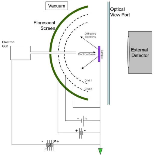
33 Figure 2.7 shows a typical setup of LEED. In the electron gun, electrons are emitted by a cathode filament with a negative potential ranging from 10 to 600 V, which is respect to the sample. Then the electrons are focus into a beam, around 0.1-0.5 mm wide, by a series of electron lenses. Some of the electrons incident on the sample are reflected and collected by a fluorescent screen. The electric potential of the fluorescent screen rises to 3-7 kV to energize the electrons, which makes the electrons are strong enough to excite the screen. The grids, which are in between the screen and the sample, are used to cut off the inelastically scattered electrons which carry no structural information about the sample surface.
Figure 2.7: Schematic of a LEED setup. Source: https://en.wikipedia.org/wiki/Low-energy_electron_diffraction.
Theory of low-energy electron diffraction
It is very convenient to describe the interaction between scattered electrons and incident electrons in reciprocal space. In three dimensions, the correlation between the real space lattice {𝒂, 𝒃, 𝒄} and the reciprocal lattice {𝒂∗, 𝒃∗, 𝒄∗} is expressed as:
34 𝒂∗ = 2𝜋𝒃 × 𝒄 𝒂 ⋅ (𝒃 × 𝒄) (22) 𝒃∗ = 2𝜋𝒄 × 𝒂 𝒃 ⋅ (𝒄 × 𝒂) (23) 𝒄∗ = 2𝜋𝒂 × 𝒃 𝒄 ⋅ (𝒂 × 𝒃) (24)
The condition of the constructive interference is described by the Laue condition,
𝒌 − 𝒌0 = 𝑮ℎ𝑘𝑙 (25)
where 𝒌0 is the wave vector of an incident electron (𝑘0 = 2𝜋/𝜆0) and 𝒌 is the wave vector of a scattered electron (𝑘 = 2𝜋/𝜆).
𝑮ℎ𝑘𝑙 is a vector of the reciprocal lattice and can be represented by
𝑮ℎ𝑘𝑙= ℎ𝒂∗ + 𝑘𝒃∗+ 𝑙𝒄∗ (26)
where (ℎ, 𝑘, 𝑙) is a set of integers. Since elastic scattering is only considered, the magnitudes of the incident wave vector and the scattered wave vector are unchanged, |𝒌0| = |𝒌|. As we
discussed above, LEED is very sensitive to the sample surface which is due to the mean free path of the low energy electrons in a crystal. In that case, the diffraction equation (23) reduces to the two-dimensional form:
𝑮ℎ𝑘= ℎ𝒂∗+ 𝑘𝒃∗ (27)
where 𝒂∗ is perpendicular to 𝒃 with the magnitude |𝒂∗| = 1
|𝑎| sin 𝛼 , 𝒃
∗ is also perpendicular to
𝒂 with |𝒃∗| = 1
|𝑏| sin 𝛼 and 𝛼 is the angle between the real space vector 𝒂 and 𝒃.
Surface structures
Considering LEED patterns are the periodic diffraction patterns in two dimensions, the general term “surface structure” should be mentioned. A surface structure could either be the surface structure of the substrate material or could be related to the structure of a deposit [63]. Different from the atoms in the bulk, the atoms near the surface usually experience the surface reconstruction or relaxation to be stabilized. Referring to the surface reconstruction, the Wood’s notation is commonly used:
35 which describes the reconstruction of the (ℎ𝑘𝑙) plane of a material. 𝑚 and 𝑛 are given as multiples of the non-reconstructed surface unit cell vectors a and b. For example, in Figure 2.8(a) and (b), (2×2) reconstruction means that vectors of the unit cell (green balls) are twice longer than those of the unit cell of the non-reconstructed structure underneath (grey balls). Once the unit cell is rotated with respect to the unit cell of the non-reconstructed surface, the angle 𝜙 is given additionally. The example is shown in Figure 2.8(c), which indicates the unit cell of the reconstructed surface (green balls) are rotated 30˚ with respect to the unit cell of the surface underneath (grey balls).
Figure 2.8: (a) p(2×2) structure (green) on the square lattice (grey); (b) c(2×2) structure (green) on the square lattice (grey); (c) (√3 × √3)R30˚ structure (green) on the hexagon lattice (grey). In general, p indicates primitive and c indicates centered.
2.5 Near-ambient pressure X-ray photoelectron spectroscopy (NAP-XPS)
XPS is a surface-sensitive quantitative analysis technique. With the development of a high-resolution XPS by Kai Siegbahn and his research group in Uppsala University in Sweden [64], XPS allowed to measure accurate binding energy of photoelectron peaks, in which the investigation of electronic structure has been realized. The work of Kai Siegbahn was awarded by the physics Nobel prize in 1981.Principle of X-ray photoelectron spectroscopy
An XPS measurement is operated by irradiating the sample surface with a beam of monochromatic X-rays. If the photon energy is high enough, electrons from the sample atoms can be excited and create the photoelectrons, which are then emitted from the sample surface. Figure 2.9 is the schematic of a photoemission process. In this process, the electrons on a given orbital are first promoted from a bound state to an excited state by absorbing certain photon energy ℎ𝜐. Before escaping to vacuum, the photoelectrons travel some distance inside the
36 sample, in which the photoelectrons collide elastically or inelastically with the lattice atoms of the sample. The elastically scattered electrons escape from the sample surface without any kinetic energy loss, which will form the main XPS core level peak (also called adiabatic peak). On the contrary, the inelastically scattered electrons escape from the sample surface with losing a part of the kinetic energy, which will create the background of the XPS spectrum. Therefore, the surface sensitivity of XPS is determined by the electron inelastic mean free path (IMFP), which is the characteristic length that an electron on average travels through before suffering an inelastic scattering. After reaching the sample surface, the photoelectrons still need to overcome a barrier potential which exist at the sample surface in order to get to the vacuum level. That barrier potential refers to the work function of the sample.
In general, the binding energy of a photoelectron coming from the sample can be obtained by the Einstein equation:
𝐸𝑏 = ℎ𝜐 − 𝐸𝑘− Φ𝑠𝑎𝑚𝑝𝑙𝑒 (29)
where 𝐸𝑏 is the binding energy of the core level, ℎ𝜐 is the photon energy of the X-ray, , 𝐸𝑘 is the kinetic energy and Φ𝑠𝑎𝑚𝑝𝑙𝑒 is the work function of the sample.
Figure 2.9: Schematic of the photoemission process.
Particularly, when the kinetic energy is measured by the XPS analyzer (Figure 2.10), the work function of the analyzer should be considered. By grounding both the sample and the analyzer to align the Fermi level, the equation (29) can be rewritten as:
37 where 𝐸𝑏 is the binding energy of the core level, ℎ𝜐 is the photon energy of the X-ray, , 𝐸𝑘 is the kinetic energy and Φ𝑎𝑛𝑎𝑙𝑦𝑧𝑒𝑟 is the work function of the analyzer.
Figure 2.10: Schematic of the sample and analyzer energy level.
The binding energy of a core electron measured by XPS is influenced by the interactions between the electron and the surrounding environment, which are Coulomb interactions with other electrons and the attraction from the nuclei. Changes in the chemical environment have an influence on the valence electron of the element, which then lead the electrons to a spatial redistribution and affect the value of the binding energy of the core electron. Consequently, the variation of the binding energy of the core electron is observed as a shift on the XPS peak of the core electron, which is called the chemical shift (Δ𝜉). Due to the advantage of XPS, chemical shift can be easily interpretable in XPS spectrum with a well-defined energy position, such as the different oxidation state and different chemical environment.
Due to the spin-orbit splitting effect, all orbital levels (except s orbital) will show two spin-orbit splitting peaks in XPS spectrum, i.e. doublet pairs. Based on the quantum mechanics, the total angular momentum ( 𝑗 ) is expressed as:
𝑗 = 𝑙 + 𝑠 (31)
where 𝑙 is the orbital angular momentum ( 𝑙 = 1 for p orbital, 𝑙 = 2 for d orbital and 𝑙 = 3 for f orbital) and 𝑠 is the spin angular momentum (𝑠 = ±1/2). The formula (31) gives two values 𝑗1 and 𝑗2, which corresponds to the two peaks due to splitting, respectively. (e.g. 𝑛𝑓5/2 and 𝑛𝑓7/2, where 𝑛 is the principal quantum number.) Moreover, the relative intensities of the doublet pairs are given by 𝑗1+1
𝑗2+1. Thus, for p electrons the relative intensities are 1: 2 , while for
38 Also, the energy separation of the doublet pairs depends on both the principal (𝑛) and angular momentum (𝑗) of the core level electrons and can result in widely separated doublet pairs.
Description of X-ray photoelectron spectroscopy
Figure 2.11 shows the schematic of the XPS principal in UHV. Basically, the XPS system consists of three critical components, which are the X-ray source, the electron analyzer and the detector with appropriate signal counting electronics. Electrons are first emitted from the sample surface by the X-ray source (usually Mg/Al X-ray sources). Then they are supposed to decelerate or accelerate by the electrostatic lenses in the analyzer to the pass energy Ep and focus on the inlet slit. The potentials applied to the inner and outer hemisphere of the electron analyzer correspond to a selection of electrons with the kinetic energy Ep. Therefore, the photoelectrons are registered in a small kinetic energy range, which determines the resolution of the analyzer. Electrons are finally detected by the electron multiplier of the detector in pulse counting mode.
39 The XPS system should be kept in UHV because the photoelectron signal will be strongly decreased by the interaction of the photoelectrons with the atmosphere if the vacuum is not good enough. Standard XPS systems operate in a vacuum in the low 10-10 mbar range. Although the inelastic mean free path (IMFP) of electrons in the gas phase is determined by the kinetic energy of electrons and the gas pressure, the count rate of detected photoelectrons is exponentially decreasing with increasing the pressure of atmosphere, as shown in Figure 2.11. For example, electrons with a kinetic energy 100 eV have an IMFP around 1 mm in 1 mbar gas phase. Besides, the sample should also be kept in UHV to be clean because the sample surface will be contaminated by the gas phase if the vacuum is bad.
Figure 2.11: XPS signal versus increasing pressure [65].
Description of near-ambient pressure X-ray photoelectron spectroscopy
Due to the exponential decrease of the photoelectron signal in gas phase, NAP-XPS technique is designed to partially overcome the pressure gap in surface science. Unlike the ordinary XPS, NAP-XPS allows the sample to be exposed in high pressures in order of millibars, which can study the dynamics of catalytic reactions. The most significant change for NAP-XPS is the introduction of the differential pumping in the electron analyzer system which dramatically decreases photoelectron attenuation between the sample and the analyzer. The early design of the differential pumping system is shown in Figure 2.12 (a). In this design, the photoelectrons travel through differential pumping regions before reaching the analyzer, which are unfocused between the apertures. The unfocused photoelectrons would cause a serious loss in collection efficiency. Fortunately, the new design of the differential pumping system (Figure 2.12 (b)) is combined with a series of electrostatic lenses which greatly increase the electron collection rate. Different from the laboratory X-ray source (Al/Mg source) used in the XPS, the
40 synchrotron-based light is applied onto the NAP-XPS, which can produce a high flux of photons and a more focalized size at the sample generating more photoelectrons. Nowadays, a number of synchrotron-based NAP-XPS setups have arisen all over the world, such as SOLEIL, DIAMOND, BESSY, ALS and SSRL [66].
Figure 2.12: Schematic of photoelectron path from the sample to the analyzer entrance. (a) Early design of differential pumping system and (b) the new design of the differential pumping system with electrostatic lens (green lines) [67].
A schematic diagram of the SOLEIL synchrotron is shown in Figure 2.13. Several steps are involved to obtain the synchrotron radiation. First, the electron beam is emitted by the electron gun, which is then accelerated by the linear accelerator to 10 MeV. The electrons are further accelerated to 100 MeV in the booster ring and up to a maximum energy of several GeV in the storage ring where the electrons are stored. When the electron beam circulates in the storage ring, the trajectory of the electron beam is altered by the diploe magnets and the electron beam is focused by the quadrupole magnets after the change of the trajectory. The beamlines, the end stations, are installed tangentially to take advantage of the synchrotron light for experiments. Comparing to the laboratory X-rays, the synchrotron light has a very broad spectral range, which covers from microwaves to hard X- rays. Thus, the photon energy can be selected based on different experiments. As for the TEMPO beamline, the synchrotron beam, a high flux of photons with the energy range from 50 to 1500 eV, is introduced into the analysis chamber of the NAP-XPS through a Si3N4Al window in order to keep the beam in UHV (the pressure range of 10-9 mbar).The beam spot has a diameter of 0.1 mm on the sample in the analysis chamber, which makes an angle of 54˚ with the sample normal.
41 Figure 2.13: Diagram of SOLEIL synchrotron radiation facility in France. Source: https://www.synchrotron-soleil.fr/fr/recherche
Figure 2.14 shows the NAP-XPS at the TEMPO beamline, which is composed of several chambers, i.e. the load lock, the preparation chamber, the analysis chamber and the catalysis chamber (not shown in Figure 2.14). Especially, the analysis chamber is the gold coated mu-metal chamber which equipped with 7 lines inlets. Five lines are reserved for dosing gases, in which four for pure gases and one for mixed gases. The other two lines are used as dosing liquid like water for example. The sample stage is mounted on a vertical manipulator (the inset of Figure 2.14), which is mainly dedicated to catalysis reactions as the sample can be heated up to 1000 ℃ in the atmosphere of the reactive gases (the maximum working pressure 20 mbar) allowing to investigate the in situ catalytic reactions.

![Figure 1.2: Primary air pollutants and their sources [1].](https://thumb-eu.123doks.com/thumbv2/123doknet/14668999.741368/9.892.121.771.170.583/figure-primary-air-pollutants-sources.webp)