HAL Id: hal-03047338
https://hal.archives-ouvertes.fr/hal-03047338
Submitted on 10 Dec 2020HAL is a multi-disciplinary open access archive for the deposit and dissemination of sci-entific research documents, whether they are pub-lished or not. The documents may come from teaching and research institutions in France or abroad, or from public or private research centers.
L’archive ouverte pluridisciplinaire HAL, est destinée au dépôt et à la diffusion de documents scientifiques de niveau recherche, publiés ou non, émanant des établissements d’enseignement et de recherche français ou étrangers, des laboratoires publics ou privés.
Deposition of Sb2Se3 thin films on Pt substrate via
electro-chemical atomic layer epitaxy (EC-ALE)
Fatima Haidar, Annie Pradel, Yuan Chen, Marie-Christine Record
To cite this version:
Fatima Haidar, Annie Pradel, Yuan Chen, Marie-Christine Record. Deposition of Sb2Se3 thin films on Pt substrate via electro-chemical atomic layer epitaxy (EC-ALE). Journal of Electroanalytical Chemistry, Elsevier 2020, 879, pp.114774. �10.1016/j.jelechem.2020.114774�. �hal-03047338�
Deposition of Sb2Se3 Thin Films on Pt Substrate via Electro-Chemical Atomic Layer Epitaxy (EC-ALE)
Fatima Haidar1, Annie Pradel1, Yuan Chen2,3,*, Marie-Christine Record1,4,*
1 ICGM, Univ Montpellier, CNRS, ENSCM, Montpellier, France
2 Hubei Provincial Key Laboratory of Green Light Industrial Materials, Hubei University of Technology,
Wuhan 430068, Hubei, China
3 School of Materials and Chemical Engineering, Hubei University of Technology, Wuhan 430068, Hubei,
China
4 IM2NP, UMR CNRS 7334, Aix-Marseille University, FST St Jérôme, Av. Escadrille Normandie-Niemen,
F-13013 Marseille, France. Corresponding Authors:
Yuan CHEN, [email protected] ; Marie-Christine RECORD, [email protected]
Abstract: This work deals with the deposition of a Sb2Se3 thin film on a Pt substrate using Electro-Chemical
Atomic Layer Epitaxy (EC-ALE). We first investigated the UPD of selenium on a Pt substrate. Two routes have been evidenced to get a UPD layer of Se, either the polarization of the Pt-substrate at around 0.35 V in the Se solution or the deposition of full UPD Se together with bulk deposition of Se and dissolution of the latter one at lower potentials. The following investigation on the electrochemical behavior of antimony on selenium-covered platinum electrode by cyclic voltammetry and anodic potentiodynamic studies led us to choose the two-steps procedure for the Se deposition. After an optimization of the deposition parameters, the alternate deposition of Sb and Se elements to form the Sb2Se3 compound by
EC-ALE on platinum substrate has been performed. The stoichiometry of the deposited film has been evaluated by coulometry and it has been confirmed by atomic force microscopy (AFM).
Keywords: Underpotential deposition; EC-ALD; Cyclic voltammetry; Coulometry; AFM; Sb2Se3;
Introduction
Sb2Se3 is a V-VI semiconductor with a layered crystal structure (space group Pnma; n°62) [1]. This
compound is interesting as a thermoelectric material on two counts: first, it has a Seebeck coefficient of 46.2 μV/K in its polycrystalline form [2], and second, it is a component of the solid solutions
(Bi,Sb)2(Te,Se)3, which are the best materials used to date for cooling applications [3-7]. In addition, it also
has promising applications in several other fields such as optoelectronic, photovoltaic and batteries. As a consequence, both elaboration and characterization of this compound have been widely studied (see for example Ref. [8-13]). Miniaturization of the thermoelectric devices requires the use of thin films, which are usually prepared by physical methods under vacuum. Electrochemical deposition may provide an alternative process to these classical methods. Indeed, by contrast to other methods, electrochemical deposition is a low cost, room temperature production technique, which allows one to cover substrates with complex shapes. Some studies have already been reported on electrochemical deposition of Sb2Se3
[14-17]. Compared to other electrochemical methods, EC-ALE allows one to obtain deposits with flat surface which can easily be used for instance in the elaboration of superlattices. These nanostructures exhibit the highest Seebeck coefficients so far. The Electrochemical Atomic Layer Epitaxy (EC-ALE) technique, which was put forward by J. Stickney [18], was used in a previous work to deposit Sb2Se3 on a
polycrystalline gold substrate [19]. This method is based on the alternate underpotential deposition (UPD) of atomic layers of the elements to make up a compound, advantageously combining the technique of electrochemical deposition and that of atomic layer epitaxy (ALE). Since separate solutions and potentials are used to deposit atomic layers of each element, all the steps of each cycle can be investigated and optimized independently. Ideally, one cycle of deposition results in the formation of one compound monolayer, the number of cycles determining the overall thickness of the complete electrochemical deposit. The process of electrodeposition is highly related to the nature of the substrate. However, in spite of the wide utilization of platinum as substrate material for electrodeposition, only few investigations involving this substrate have been carried out in the field of EC-ALE [20-22] and none of them concern the Sb2Se3 deposition. We recently investigated the deposition of Se and Sb on Pt substrates
[23]. It was shown that the Se-UPD layer with full coverage could be directly formed on a Pt substrate. The cyclic voltammograms also showed that the two-step method needed for Se-UPD deposition on Au substrate [19], which consisted in the deposition of UPD together with bulk Se followed by the dissolution of bulk Se, could also be carried out on Pt substrate. The Sb underpotential deposition on Pt substrate is much more complex. It implies a multi-step process including an unavoidable preliminary adsorption of SbO+ species on the Pt electrode, followed by their reduction to metallic Sb and further underpotential
deposition of Sb on this Sb-modified Pt electrode to increase the coverage of the metallic Sb monolayer. In this work, based on these previous results [23], we investigated the electrochemical behavior of antimony on a selenium-covered platinum electrode by means of cyclic voltammetry, anodic
potentiodynamic measurements and coulometry, and performed the EC-ALE process to elaborate Sb2Se3
thin films that we characterized by coulometry and atomic force microscopy (AFM). 1. Materials and methods
1.1. Reagents
Solutions were prepared using ACS reagent grade or higher-grade chemicals (Sigma-Aldrich, Inc., USA) and deionised water (Milli-Q > 18.2 MΩ∙cm, Merck KGaA, Darmstadt, Germany). In this study three different solutions have been used: 1) the antimony solution containing Sb2O3 (99.999%) and the supporting
electrolyte Na2SO4, with concentration of 0.05 mM and 0.2 M, respectively; 2) the selenium solution
containing SeO2 (99.999%) and Na2SO4, with concentration of 0.5 mM and 0.2M, respectively; 3) the blank
solution consisting in supporting electrolyte solution with same pH and ionic strength as the ones of deposition solutions. This latter one was used to rinse the electrochemical cell. The concentrations of Sb2O3 and SeO2 were chosen based on both literature data and experimental observations. The
concentration used in literature for Sb2O3 solutions [20, 24-30] ranges from 0.01 mM to 0.05mM, and we
can confirm from experiment that 0.05 mM which is the most often used concentration, is higher than the solubility limit of antimony oxide in sulfuric acid solution. The concentration used in literature for SeO2
solutions [22, 31-43] ranges from 0.05 mM to 2 mM, with 0.5 mM as the most often used one. The pH values for all the solutions were adjusted to 1.00 with H2SO4. All the solutions were freshly prepared and
degassed for 30 minutes with pure Ar gas (Ar Bip, O2 < 10 ppb, Air Products and Chemicals, Inc., France)
just before starting each series of measurements. All the solutions were maintained under Ar atmosphere during the experiments, which were performed at room temperature.
1.2. Substrates
The platinum substrates consisted of quartz slides, coated with 200 nm thick platinum films (99.9% pure) by physical vapor deposition. A thin layer of Cr (25 nm) was beforehand deposited under the Pt film to improve the adhesion of platinum onto quartz. Before use, the platinum substrates were first annealed at 375 °C for 18 h in sealed glass tubes under vacuum (10-6 Torr) and then soaked in hot nitric acid for 5
min. Before each experiment, in order to clean and check the substrate, cyclic voltammetry (CV) scanning (repeated 25 times) of the Pt substrate in 0.1 M H2SO4 solution was performed with potential varying from
−0.27 to 1.20 V. The real area of the Pt electrode was estimated to be 3.79 cm2. This estimation was done
from the I-t curve of CV by integrating the reduction peaks of adsorbed hydrogen ions (see our previous paper [23]).
1.3. Electrochemical equipment
All the electrochemical experiments were performed with the EC-ALE equipment developed in our group and described in our previous works [19,44]. In the electrochemical cell, a platinum sheet (Sigma-Aldrich, Inc., USA) is used as counter electrode. The working electrode is made of platinum substrate. All electrochemical potential values are measured with respect to the potential of an Ag/AgCl reference electrode (3.0 M NaCl, 0.209 V vs. standard hydrogen electrode (SHE), Ametek, Inc., USA). The atomic layer deposition of Se and Sb elements was electrochemically studied by means of cyclic voltammetry, anodic potentiodynamic scanning and coulometry.
1.4. Deposit characterization
The Sb2Se3 thin films were characterized by coulometry and atomic force microscopy (AFM). The AFM
measurements were performed with a Bruker Nanoscope Dimension 3100 atomic force microscope (AFM, Bruker, Palaiseau, France) in the tapping mode under ambient conditions. The cantilever tips were Silicon Point Probe Plus NCSTR (Nanosensors, Neuchâtel, Switzerland; force constant 6.5 N/m, resonance frequency 157 kHz). All the image treatments were performed using Gwyddion [45].
2. Results and discussion
As noted in the Introduction section, the formation of both Sb and Se atomic layers on Pt was already investigated in our previous paper [23]. The results are as follows.
As it was shown in literature [46-52] that antimony can adsorb irreversibly on Pt surface by simply immersing Pt electrode in a solution containing SbO+ ions at the OCV, we designed the following
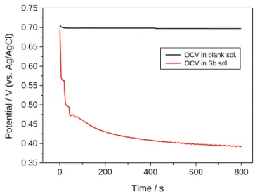
experimental procedure to adsorb adequate Sb species on a clean Pt electrode : (i) Before the beginning of the experiments, the clean Pt electrode is placed in the electrochemical cell filled with blank solution ; (ii) the Sb solution is introduced into the electrochemical cell and kept flowing for 5 s. Then the Sb solution is kept still for 15 s ; (iii) the step (ii) as a cycle is repeated totally for 40 times, and the variation of the OCV of Pt electrode during this process is recorded (see red curve in Figure 1) ; (iv) as a control, a similar experiment procedure is performed as steps (i) to (iii), but during the whole process the blank solution is used instead of the Sb solution. The evolution of the OCV of Pt electrode during this process is shown as the black curve in Figure 1.
From the results shown in Figure 1, one can see that the OCV of Pt electrode decreases continuously in the Sb solution, indicating that Sb species (SbO+) are indeed adsorbed irreversibly on Pt electrode. Before
the beginning of the experiments, the clean Pt electrode is kept in the electrochemical cell filled with blank solution, where the OCV is approximately 0.70 V. The high OCV is due to the chemical oxygen Ochem
adsorbed on Pt electrode in an acid solution environment according to the literature [46]. When the Sb solution is introduced into the cell, the SbO+ species are irreversibly adsorbed on Pt and replace the
adsorbed chemical oxygen Ochem at their sites, leading to the structural change of the double-layer on the
surface of Pt electrode. The structural change of the double-layer leads to the change of OCV. Therefore, the decrease of the OCV demonstrates the occurrence of the irreversible adsorption of Sb species. The OCV of Pt electrode in Sb solution approximately reaches a plateau after 800 s (40 cycles), indicating that the amount of irreversibly adsorbed Sb species reaches a maximum. This observation also illustrates that the irreversible adsorption process of Sb species on Pt substrate is kinetically slow, or in other words, the process of replacing Ochem by SbO+ species is kinetically slow.
At the opposite, the underpotential deposition of Se on Pt substrate was quite straightforward. Therefore, in the present work, we started the alternate deposition of Sb and Se elements by first depositing Se atomic monolayer onto the Pt electrode.
0 200 400 600 800 0.35 0.40 0.45 0.50 0.55 0.60 0.65 0.70 0.75
OCV in blank sol. OCV in Sb sol. Time / s Poten tia l / V (vs . Ag/Ag Cl)
Figure 1. Evolution of the OCV of Pt electrode during the irreversible adsorption process of Sb (red curve) compared to a reference experiment with blank solution (black curve).
2.1. UPD of Selenium on Pt substrate (Pt/Se)
The underpotential deposition of Se element on Pt substrate was carried out on the basis of our previous investigation reported in [23]. At the time, it was shown that the underpotential deposition of Se occurred at 0.48 V (with respect to the potential of Ag/AgCl reference electrode) and its bulk deposition occurred
at 0.24 V, which leads us to conclude by comparison with results of ref. [53], that Se is preferentially deposited onto Pt(111). As with the UPD of Se on Au substrate [19], two additional reductions were evidenced at lower potentials: 1) the reduction of 3-D bulk-deposition of Se to H2Se, which is soluble, at
-0.34V, 2) the formation of red Se due to the coexistence in the cell of HSeO3- and H
2Se at -0.4V. Therefore
there are two possibilities to get a UPD layer of Se, either the polarization of the Pt-substrate at around 0.35 V in the Se solution or the deposition of full UPD Se together with bulk deposition of Se and dissolution of the latter one at lower potentials. For the first Se layer, both procedures are relevant. However, a polarization at 0.35 V cannot be used for the deposit in the subsequent cycles since the stripping of UPD-Sb on Se-covered Pt substrate starts occurring below 0.35V, as demonstrated below in section 2.2. Therefore, the two-steps procedure was used in the present work. The potential window to deposit both UPD and bulk Se is [-0.25V, 0.1V] as evidenced in [23]. Thus, the procedure for the first layer deposition will be as follows: i) the Pt electrode is rinsed for 15 s in the Se solution at OCV and kept for 10 s in this solution at 0 V to deposit the bulk Se ; ii) while the electrode is maintained at the same potential the cell is rinsed with blank solution for 10 s to get rid of HSeO3- ions in order to avoid the formation of
red Se ; iii) the potential is moved down to – 0.36 V and maintained at this value for 10 s while the blank solution is rinsing such that bulk Se is reduced to HSe-.
2.2. UPD of antimony on Se-covered Pt substrate (Pt/Se/Sb)
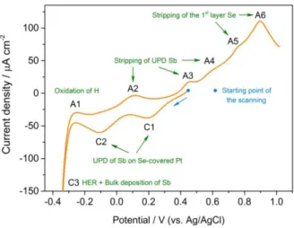
The investigation of the UPD of antimony on Se-covered Pt was performed as follows: (i) the previously prepared UPD Se-covered electrode was kept at 0.45 V, a potential where the UPD-Se layer is stable, while the Sb solution was introduced into the cell; (ii) the UPD Se-covered electrode was scanned from 0.45 V to −0.35 V and positively back to 1.05 V.
Figure 2 shows the CV curve of the Se-covered Pt electrode in Sb solution. C1 and C2 peaks are assigned to the UPD peaks of Sb on Se-covered Pt electrode and A2, A3 and A4 their corresponding stripping peaks. Such assignment is based on a detailed study of the peak evolution during anodic potentiodynamic scanning after different polarizations reported in the following part of the present section. In agreement with previous results [18], the additional peaks appearing in the anodic part of the curve in the range [0.7V – 1V] correspond to the stripping peaks of Se UPD on the Pt electrode. No peak that could be assigned to bulk Sb deposition or stripping, is observed in the CV curve. It could be due to the fact that bulk Sb deposition, which is closely related to the concentration of the solution (0.05 mM), is slow and cannot occur to a large extent during a relatively fast cyclic voltammogram (20 mV/s). This assumption is
supported by the results presented just below that show the need for long polarization duration to observe the appearance of the stripping peak of bulk Sb. One can find similar electrochemical behavior of antimony in the literature [26-27,54-55].
Figure 2. Voltammograms of Se-covered Pt substrate in the Sb solution at pH 1.0. The scanning rate is 20 mV/s.
In order to determine the optimum potential for Sb UPD onto Se-covered Pt, i.e. the potential leading to a high coverage of Sb UPD while avoiding the Sb bulk deposition, we performed an anodic potentiodynamic scanning experiment. The Se-covered Pt electrode was polarized for 20 s at various potentials (from -0.16 V to -0.26 V) while the Sb solution was kept flowing through the cell to provide enough Sb ions. Then the cell was rinsed by the blank solution and the anodic potential scanning was performed up to 1.05 V. The current curves are given in Fig. 3a. When the polarization potential was equal or higher than -0.20 V, five peaks (A2 - A6) only were observed on the curve.
For potentials equal or lower than -0.21 V an additional peak, A1, could be seen and its intensity increased as the polarization potentials decreased. Therefore, the peak A1 should correspond to the oxidative stripping peak of the bulk deposited Sb. According to these results, a potential higher than -0.20 V has to be chosen for the UPD Sb on Se-covered Pt substrate.
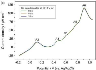
Since the Sb concentration of the solution is low (0.05 mM), the Sb bulk deposition should be slow. However, to ensure that bulk deposition of Sb was avoided, we performed two additional experiments. The Se-covered Pt electrode was polarized for different durations at -0.20 V (Fig. 3b) and -0.19 V (Fig. 3c)
in a flowing Sb solution to provide enough Sb ions, then the cell was rinsed with blank solution and an anodic potential scanning was performed up to 1.05 V with a scanning rate of 20 mV/s.
Figure 3. Anodic potentiodynamic scanning curves of the Se-covered Pt substrate obtained in the blank solution at pH 1.0: i) after polarization for 20 s at various potentials (Fig. 3a); ii) after polarization for different durations, at -0.20 V (Fig. 3b), at -0.19 V (Fig. 3c). In all cases, the polarizations were performed in a flowing Sb solution and the cell was rinsed before the anodic potentiodynamic measurements. The scanning rate was 20 mV / s.
As shown in Fig. 3b, the A1 peak corresponding to the oxidation of the bulk Sb deposition is observed when the polarization potential is -0.20 V for a time duration of 40 s and 60 s. By contrast, when the polarization potential is -0.19 V, irrespective of the time duration, this peak does not appear (see Fig. 3c). Therefore, the ideal potential for Sb underpotential deposition on a Se-covered Pt electrode seems to be -0.19 V and the chosen procedure is as follows. After having rinsed the cell for 60 s with the Sb solution, the Pt electrode is kept in this solution for 10 s at -0.19 V and then rinsed with blank solution at the same potential for 15 s.
2.3. Elaboration and characterization of Se-Sb compound for three EC-ALE cycles (6 atomic layers) 2.3.1. Alternative deposition of Se and Sb
The underpotential deposition parameters for the first three EC-ALE cycles were defined based on the above results. They are given in Table 1.
The potential window to deposit both UPD and bulk Se is [-0.25V, 0.1V] as evidenced in [18]. Thus, during the second and third cycles, in order to narrow the potential variations in the system, a potential similar to the value used for Sb UPD was used for the Se deposition.
Owing to changes in the atom environment and in the film resistance during the completion of the successive depositions, the deposition parameters had to be adjusted and are thus somewhat different from cycle to cycle.
Generally, as the alternative deposition progresses, the deposited part will generate additional resistance [26-27,54-55], which will cause the deposition potential to shift negatively. In our experiments, we tried different negatively-shifted potentials for deposition, and then determined the deposition potential of each layer according to the amount of stripping from anodic potentiodynamic scanning curve. The optimization of the experimental parameters has to be done at the beginning of the deposition. After three cycles, the latter values can be used for all the subsequent cycles, which is why we limited the deposition to 3 cycles.
For each cycle in step 1, the solution containing the reactant (I for Se, II for Sb) is introduced into the cell and is kept flowing in it during few seconds to properly fill in the cell. Step 2 corresponds to the deposition one ; the solution is then maintained static to avoid perturbations in the process. In step 3, the cell is rinsed with the blank solution flowing in it for few seconds. In step 4, when relevant, the applied potential is greatly reduced to dissolve bulk Se.
Table 1. Electrodeposition parameters of the first three EC-ALE cycles for Sb-Se compound
Cycles Elements Step 1 Step 2 Step 3 Step 4
Cycle 1 Se I, OCV, 15 s Is, 0 V, 15 s III, 0 V, 10 s III, -0.36 V, 10 s Sb II, -0.19 V, 60 s IIs, -0.19 V, 10 s III, -0.19V, 15 s
Cycle 2 Se I, -0.19 V, 15 s Is, -0.19 V, 15 s III, −0.19 V, 10 s III, −0.40 V, 10 s Sb II, −0.20 V, 45 s IIs, -0.20 V, 25 s III, -0.20 V, 15 s
Sb II, −0.20 V, 45 s IIs, -0.20 V, 25 s III, -0.20 V, 15 s
I, II, and III represent the flowing Se, Sb, and blank solutions, respectively. Is and IIs represent the static Se and Sb solution, respectively. OCV: open circuit voltage
After each cycle, an anodic potentiodynamic scanning was performed. The corresponding curves are plotted in Fig.4. In all cases, the stripping peaks of both Sb and Se can be observed. For the first layer the curve is in agreement with those presented in Figure 3. There are 3 stripping peaks at around 0.1 V, 0.45 V and 0.6 V for Sb and 2 stripping peaks at around 0.75 V and 0.9 V for Se. For the subsequent layers, additional peaks appear around 0.6V, they can be related to the stripping of Se atoms deposited onto Sb ones.
Figure 4. Anodic potentiodynamic scanning curves obtained after each cycle (Se + Sb) 2.3.2. Coulometry analysis
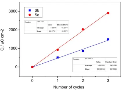
After deposition, each atomic layer is immediately removed using the blank solution, and the amount of electric charges is calculated by integrating the corresponding oxidative peak in current-time curve while deducting the background current. The results are shown in Fig. 5. As expected, the calculated charges for both Se and Sb deposits increase linearly with the number of cycles. The corresponding slopes are 981 μC cm−2 and 482 μC cm−2, respectively. The coverage rate for both Se and Sb can be estimated from these
Figure 5. Charges involved in the oxidative stripping of Se and Sb as a function of the number of EC-ALE cycles.
Since the reduction of Se and Sb involves four and three electrons, respectively, the determination of the stripping charges leads to a stoichiometric ratio of 3.06:2 for Se to Sb. This stoichiometric ratio approximates that of the Sb2Se3 compound.
2.3.3. Atomic Force Microscopy
The morphology of the deposited layer analyzed by AFM is shown in Figure 6a along with the morphology of the Pt substrate in Figure 6b. As expected, the average roughness increases from the bare Pt substrate (2.63 nm) to that of the deposit layer (3.45 nm). No information on the coverage rate can be obtained from these results, however by measuring the contact potential difference (CPD) we are able to determine the work function of the sample surfaces and evaluate the stoichiometry of the deposit.
If the work function of the sample surface differs from that of the tip, an electrostatic force originating from the adjustment of the Fermi levels between the tip and the sample occurs when the applied voltage between the tip and the sample is zero. When the applied voltagecorresponds to the work function difference, no electrostatic force occurs. When oscillating the tip voltage, the gradient of the electrostatic force is modulated and detected as frequency shift of cantilever resonance frequency [56].
a) b)
Figure 6. Atomic force microscopy (AFM) micrographs of (a) 3 cycle-Sb-Se deposit on Pt substrate and (b) bare Pt substrate.
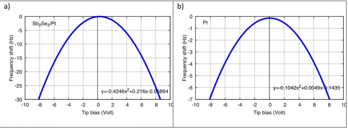
Figure 7 shows the shift in frequency of the cantilever resonance as a function of the bias voltage applied to the tip to null out the contact potential for the Pt/tip system (Fig. 7a) and for the Sb2Se3-Pt/tip system
(Fig. 7b). In each case, the data are well fitted with a quadratic function; the corresponding equations are given in the figure. This evolution agrees with the quadratic variation of the electrostatic force with the applied bias voltage [57]. The maximum of the frequency shift corresponds to a voltage of -23,5 mV for the Pt/tip system and of 255 mV for the Sb2Se3-Pt/tip one. The bias voltage is much higher for the Sb2Se3
-covered Pt substrate. Since the contact potential is due to the difference in work function between the tip and the sample, the work function of the deposit can be calculated as follows: Ws (deposit) = - e. V (Sb2Se3-Pt/tip) - e. V (Pt/tip) + Ws (Pt) = 5.42 eV
V (Sb2Se3-Pt/tip) and V (Pt/tip) are the bias voltages of the two systems and Ws (Pt) is the work function
of Pt. The value of the work function for platinum equals 5.65 eV [58]. By using the work functions of Sb and Se (4,7 eV and 5,9 eV, respectively), the work function of Sb2Se3 can be evaluated with the following
relation: Ws (Sb2Se3) = [2 x Ws(Sb) + 3 x Ws(Se) ] /5. Its value amounts to 5.42 eV, which is identical to the
calculated one from measurements (see above). This result supports that the deposit obtained via EC-ALE corresponds to the expected compound, Sb2Se3.
a) b)
Figure 7. Frequency shift vs. bias voltage with the tip placed above (a) the Sb2Se3-Pt system, (b) the Pt
substrate. The data are fitted with a quadratic function. Conclusion
Voltammetry, anodic potentiodynamic scanning and coulometry experiments have been performed to optimize the electrochemical deposition parameters for Sb-Se thin films on platinum substrates. Based on previous results regarding the electrochemical behaviors of selenium and antimony on bare platinum electrode, the electrochemical behavior of antimony on a selenium-covered platinum electrode has been investigated and once the parameters optimized, the alternate deposition of Sb and Se elements by EC-ALE has been carried out. By using coulometry and AFM measurements, it was shown that the stoichiometry of the Sb-Se deposit corresponds to that of Sb2Se3.
References
[1] O. Madelung, Semiconductors: other than group IV elements and III-V compounds. Germany: Springer-Verlag, 1992.
[2] K.Y. Rajpure, C.D. Lokhande and C.H. Bhosale, A comparative study of the properties of spray-deposited Sb2Se3 thin films prepared from aqueous and nonaqueous media. Materials Research Bulletin, 34 (7) (1999) 1079-1087. https://doi.org/10.1016/S0025-5408(99)00095-1
[3] H.W. Jeon, H.P. Ha, D.B. Hyun, J.D. Shim, Electrical and thermoelectrical properties of undoped Bi2Te3-Sb2Te3 and Bi2Te3-Sb2Te3-Sb2Se3 single crystals. Journal of Physics and Chemistry of Solids, 52 (4)
(1991) 579-585. https://doi.org/10.1016/0022-3697(91)90151-O
[4] W.M. Yim and F.D. Rosi, Compound tellurides and their alloys for Peltier cooling – A review. Solid-State Electronics, 15 (10) (1972) 1121-1140. https://doi.org/10.1016/0038-1101(72)90172-4
pseudo-ternary alloys in the temperature range 77 to 300° K. Journal of Materials Science, 1 (1) (1966) 52-65. https://doi.org/10.1007/BF00549720
[6] F.D. Rosi, B. Abeles, and R.V. Jensen, Materials for thermoelectric generation. Journal of Physics and Chemistry of Solids, 10 (2–3) (1959) 191-200. https://doi.org/10.1016/0022-3697(59)90074-5
[7] X.B. Xiao, T.J. Zhu, and X.H. Ji, Thermoelectrics Handbook: Macro to Nano, Ed. D.M. Rowe. CRC, Boca Raton, FL, 2006: p. 25.
[8] A.M. Fernández and M.G. Merino, Preparation and characterization of Sb3Se3 thin films prepared by
electrodeposition for photovoltaic applications. Thin Solid Films, 366 (1–2) (2000) 202-206. https://doi.org/10.1016/S0040-6090(00)00716-1
[9] K.Y. Rajpure and C.H. Bhosale, Preparation and characterization of spray deposited photoactive Sb2S3
and Sb2Se3 thin films using aqueous and non-aqueous media. Materials Chemistry and Physics, 73 (1)
(2002) 6-12. https://doi.org/10.1016/S0254-0584(01)00350-9
[10] D. Wang, D. Yu, M. Mo , X. Liu, Y. Qian, Preparation and characterization of wire-like Sb2Se3 and
flake-like Bi2Se3 nanocrystals. Journal of Crystal Growth, 253 (1–4) (2003) 445-451.
https://doi.org/10.1016/S0022-0248(03)01019-4
[11] M.-Z. Xue and Z.-W. Fu, Pulsed laser deposited Sb2Se3 anode for lithium-ion batteries. Journal of
Alloys and Compounds, 458 (1–2) (2008) 351-356. https://doi.org/10.1016/j.jallcom.2007.03.109 [12] L. Yu, J. Chen, and Z.-W. Fu, Pulsed laser deposited heterogeneous mixture of Li2Se–Sb2Se3
nanocomposite as a new storage lithium material. Electrochimica Acta, 55 (3) (2010) 1258-1264. https://doi.org/10.1016/j.electacta.2009.10.046
[13] X. Wang, K.F. Cai, F. Shang, S. Chen, Preparation and electrical transport properties of
nanostructured Sb2Se3 films fabricated by combining spin-coating and gas-induced reduction. Journal of
Nanoparticle Research, 15 (4) (2013) 1541-1-1541-8. https://doi.org/10.1007/s11051-013-1541-5 [14] J.D. Desai and K.N. Ganage, Electrodeposition of Sb2Se3 thin films from alkaline bath. Bulletin of
Electrochemistry., 15 (7-8) (1999) 318-320.
[15] A.P. Torane and C.H. Bhosale, Preparation and characterization of electrodeposited Sb2Se3 thin films from non-aqueous media. Journal of Physics and Chemistry of Solids, 63 (10) (2002) 1849-1855. https://doi.org/10.1016/S0022-3697(02)00167-1
[16] X. Shi, X. zhang, Y. Tian, C. Shen, C. Wang, H-J Gao, Electrodeposition of Sb2Se3 on indium-doped tin
oxides substrate: Nucleation and growth. Applied Surface Science, 258 (6) (2012) 2169-2173. https://doi.org/10.1016/j.apsusc.2011.02.097
[17] Y. Lai, C. Han, X. Lv, J. Yang, F. Liu, J. L, Y. Liu, Electrodeposition of antimony selenide thin films from aqueous acid solutions. Journal of Electroanalytical Chemistry, 671 (0) (2012) 73-79.
https://doi.org/10.1016/j.jelechem.2012.02.018
[18] B. W. Gregory and J. L. Stickney, Electrochemical atomic layer epitaxy (ECALE). Journal of Electroanalytical Chemistry & Interfacial Electrochemistry, 300 (91) (1991) 543-561.
https://doi.org/10.1016/0022-0728(91)85415-L
[19] Y. Chen, L. Wang, A. Pradel, A. Merlin, M. Ribes and M.-C. Record, Underpotential deposition of selenium and antimony on gold. Journal of Solid State Electrochemistry, 19(8) (2015) 2399-2411. https://doi.org/10.1007/s10008-015-2881-0
[20] J.Y. Yang, W. Zhu, X. Gao, S. Bao, X. Fan, X. Duan and J. Hou, Formation and characterization of Sb2Te3 nanofilms on Pt by electrochemical atomic layer epitaxy. Journal of Physical Chemistry B, 110 (10) (2006) 4599-4604. https://doi.org/10.1021/jp0565498
[21] W. Zhu, J.Y.Yang, X.H.Gao, S.Q.Bao, X.A.Fan, T.J.Zhang and K.Cui, Effect of potential on bismuth telluride thin film growth by electrochemical atomic layer epitaxy. Electrochimica Acta, 50 (20) (2005) 4041-4047. https://doi.org/10.1016/j.electacta.2005.01.003
[22] C.J. Xiao, J. Yang, W. Zhu, J. Peng and J. Zhang, Electrodeposition and characterization of Bi2Se3 thin films by electrochemical atomic layer epitaxy (ECALE). Electrochimica Acta, 54 (27) (2009) 6821-6826. https://doi.org/10.1016/j.electacta.2009.06.089
[23] Y. Chen, H. Huang, Z. Wei, Y. Chang, A. Pradel, P. Boulet and M.-C. Record, A voltammetric study on the atomic layer deposition of selenium and antimony on platinum electrode. Proceedings of the 17th
International Conference on Sustainable Energy Technologies, SET2018, 21-23 August 2018, Wuhan. University of Nottingham: Buildings, Energy & Environment Research Group. (4) (2019) 219-228. [24] V. Venkatasamy, I. Shao, Q. Huang and J. Stickney, ALD approach toward electrodeposition of Sb2Te3 for phase-change memory applications. Journal of Electrochemical Society, 155 (11) (2008)
D693-D698. https://doi.org/10.1149/1.2969911
[25] J.Y. Yang, W. Zhu, X.H. Gao, X.A Fan, S.Q Bao, XK Duan, Electrochemical aspects of depositing Sb2Te3
compound on Au substrate by ECALE. Electrochimica Acta, 52 (9) (2007) 3035-3039. https://doi.org/10.1016/j.electacta.2006.09.045
[26] X.H. Gao, J.Y. Yang, W. Zhu, J. Hou, S. Bao, X. Fan and X. Duan, Deposition of antimony telluride thin film by ECALE. Science in China Series E, 49 (6) (2006) 685-692. https://doi.org/10.1007/s11431-006-2022-1
[27] W. Zhu, J.Y. Yang, D. Zhou, et al. Development of growth cycle for antimony telluride film on Au (111) disk by electrochemical atomic layer epitaxy. Electrochimica Acta, 53 (10) (2008) 3579-3586. https://doi.org/10.1016/j.electacta.2007.12.046
[28] T.L. Wade, B.H. Flowers, H., Jr, Billy, R. Vaidyanathan, K. Mathe, C.B. Maddox, U.Happek, J.L Stickney, Electrochemical atomic- layer epitaxy: electrodeposition of III- V and II- VI compound semiconductors. Materials Research Society Symposium Proceedings (2000), 581 (Nanophase and Nanocomposite Materials III), 145-150. https://doi.org/10.1557/PROC-581-145
[29] T.L. Wade, R. Vaidyanathan, U. Happek, and J.L. Stickney, Electrochemical formation of a III- V compound semiconductor superlattice: InAs /InSb. Journal of Electroanalytical Chemistry, 500 (1-2) (2001) 322-332 https://doi.org/10.1016/S0022-0728(00)00473-3
[30] W. Zhu, J.Y. Yang, D.X. Zhou, C.J Xiao, X.K Duan, Electrochemical aspects and structure characterization of VA- VIA compound semiconductor Bi2Te3/Sb2Te3 superlattice thin films via
Electrochemical Atomic Layer Epitaxy. Langmuir, 24(11) (2008) 5919-5924. https://doi.org/10.1021/la8001064
[31] T.E. Lister and J.L. Stickney, Formation of the first monolayer of CdSe on Au(111) by electrochemical ALE. Applied Surface Science, 107 (1996) 153-160. https://doi.org/10.1016/S0169-4332(96)00488-6 [32] T.E. Lister, L.P. Colletti, and J.L. Stickney, Electrochemical formation of CdSe monolayers on the low index planes of Au. Israel Journal of Chemistry, 37 (2-3) (1997) 287-295.
[33] M.K. Mathe, S.M. Cox, B.H. Flowers,Jr., R.Vaidyanathan, L. Pham, N. Srisook, U. Happek, J.L. Stickney, Deposition of CdSe by EC-ALE. Journal of Crystal Growth, 271(1-2), 55-64.
https://doi.org/10.1016/j.jcrysgro.2004.07.022
[34] F. Loglio, M. Innocenti, F. D'Acapito, R. Felicin G. Pezzatini, E. Salvietti, M.L. Foresti, Cadmium selenide electrodeposited by ECALE: electrochemical characterization and preliminary results by EXAFS. Journal of Electroanalytical Chemistry, 575 (1) (2005) 161-167.
[35] G. Pezzatini, S. Caporali, M. Innocenti, M.L. Foresti, Formation of ZnSe on Ag(111) by
electrochemical atomic layer epitaxy. Journal of Electroanalytical Chemistry, 475 (2) (1999) 164-170. https://doi.org/10.1016/S0022-0728(99)00347-2
[36] X. Zhang, X.Z. Shi, and C.M. Wang, Optimization of electrochemical aspects for epitaxial depositing nanoscale ZnSe thin films. Journal of Solid State Electrochemistry, 13 (3) (2009) 469-475.
https://doi.org/10.1007/s10008-008-0587-2
[37] M.K. Mathe, S.M. Cox, V. Venkatasamy, U. Happek, J.L. Stickney, Formation of HgSe thin films using Electrochemical Atomic Layer Epitaxy. Journal of Electrochemical Society, 152 (11) (2005) C751-C755. https://doi.org/10.1149/1.2047547
[38] V. Venkatasamy, M.K. Mathe, S.M. Cox, U. Happek, J.L. Stickney, Optimization studies of HgSe thin film deposition by electrochemical atomic layer epitaxy (EC-ALE). Electrochimica Acta, 51 (21) (2006) 4347-4351. https://doi.org/10.1016/j.electacta.2005.12.012
[39] R. Vaidyanathan, J.L. Stickney, and U. Happek, Quantum confinement in PbSe thin films
electrodeposited by electrochemical atomic layer epitaxy (EC-ALE). Electrochimica Acta, 49 (8) (2004) 1321-1326. https://doi.org/10.1016/j.electacta.2003.07.019
[40] Z.Q. Qiao, W. Shang, and C.M. Wang, Fabrication of Sn–Se compounds on a gold electrode by electrochemical atomic layer epitaxy. Journal of Electroanalytical Chemistry, 576 (1) (2005) 171-175. https://doi.org/10.1016/j.jelechem.2004.10.015
[41] R. Vaidyanathan, J.L. Stickney, S.M. Cox, S.P. Compton, U. Happek, Formation of In2Se3 thin films
and nanostructures using electrochemical atomic layer epitaxy. Journal of Electroanalytical Chemistry, 559 (2003) 55-61. https://doi.org/10.1016/S0022-0728(03)00053-6
[42] R. Vaidyanathan, M.K. Mathe, P. Sprinkle, S.M. Cox, U. Happek, J.L. Stickney, Electrodeposition of Cu2Se thin films by electrochemical atomic layer epitaxy (EC-ALE). Materials Research Society
Symposium Proceedings, 2003, 744: 289-294. https://doi.org/10.1557/PROC-744-M5.34
[43] R. Vaidyanathan, S.M. Cox, U. Happek, D. Banga, M.K. Mathe, J.L. Stickney, Preliminary studies in the electrodeposition of PbSe/PbTe superlattice thin films via Electrochemical Atomic Layer Deposition (ALD). Langmuir, 22 (25) (2006) 10590-10595. https://doi.org/10.1021/la061625z
[44] Y. Chen, L. Wang, A. Pradel, M. Ribes and M.-C. Record, A voltammetric study of the underpotential deposition of cobalt and antimony on gold. Journal of Electroanalytical Chemistry, 724 (19) (2014) 55-61. https://doi.org/10.1016/j.jelechem.2014.03.025
[45] Czech Metrology Institute, Brno, Czech Republic, open software, http://gwyddion.net/ [46] Q.-H. Wu, S.-G. Sun, X.-Y. Xiao, Y.-Y. Yang, Z.Y. Zhou, An EQCM study of Sb adsorption and co-adsorption with CO on Pt electrode in perchloric acid solutions. Electrochimica Acta, 45 (22–23) (2000) 3683-3690. https://doi.org/10.1016/S0013-4686(00)00462-X
[47] E. Herrero, J.M. Feliu, and A. Aldaz, Poison formation reaction from formic acid on Pt(100) electrodes modified by irreversibly adsorbed bismuth and antimony. Journal of Electroanalytical
Chemistry, 368 (1–2) (1994) 101-108. https://doi.org/10.1016/0022-0728(93)03032-K
[48] A. Fernandez-Vega, J.M. Feliu, A. Aldaz, J. Clavilier, Heterogeneous electrocatalysis on well defined platinum surfaces modified by controlled amounts of irreversibly adsorbed adatoms: Part II. Formic acid oxidation on the Pt (100)-Sb system. Journal of Electroanalytical Chemistry and Interfacial
Electrochemistry, 258 (1) (1989) 101-113. https://doi.org/10.1016/0022-0728(89)85165-4 [49] J.M. Feliu, A. Fernandez-Vega, A. Aldaz, J. Clavilier, New observations of a structure sensitive electrochemical behaviour of irreversibly adsorbed arsenic and antimony from acidic solutions on Pt (111) and Pt (100) orientations. Journal of Electroanalytical Chemistry and Interfacial Electrochemistry, 256 (1) (1988) 149-163. https://doi.org/10.1016/0022-0728(88)85014-9
[50] N. Kizhakevariam and M.J. Weaver, Structure and reactivity of bimetallic electrochemical interfaces: infrared spectroscopic studies of carbon monoxide adsorption and formic acid electrooxidation on antimony-modified Pt(100) and Pt(111). Surface Science, 310 (1–3) (1994) 183-197.
https://doi.org/10.1016/0039-6028(94)91383-8
[51] S.G. Sun, J. Noël, J. Lipkowski, Z. Altounian, Electrocatalytic properties of glassy metals: Combined Auger electron spectroscopy and electrochemical studies of the surface composition and electrocatalysis of CO oxidation at amorphous Pt66Sb34 alloy. Journal of Electroanalytical Chemistry and Interfacial
Electrochemistry, 278 (1–2) (1990) 205-216. https://doi.org/10.1016/0022-0728(90)85134-Q
[52] S.G. Sun, J. Lipkowski, and Z. Altounian, Electrocatalytic Oxidation of Formic Acid and Methanol at the Amorphous Pt66Sb34 Electrode. Journal of Electrochemical Society, 1137 (8) (1990) 2443-2451.
https://doi.org/10.1149/1.2086958
[53] S. Iqbal, C. Bondü, H. Baltruschat, Quantitative Determination of H2Se at Model Metal fcc(111)
Selenide Surface: DEMS, STM, and AFM Studies. The Journal of Physical Chemistry C, 119(35) (2015) 20515–20523. https://doi.org/10.1021/acs.jpcc.5b06635
[54] J.Y. Yang, W. Zhu, X.H. Gao, X.A. Fan, S.Q. Bao, X.K. Duan, Electrochemical aspects of depositing Sb2Te3 compound on Au substrate by ECALE. Electrochimica Acta, 52 (9) (2007) 3035-3039.
https://doi.org/10.1016/j.electacta.2006.09.045
[55] J.Y. Yang, W. Zhu, X.H. Gao, S. Bao, X. Fan, X. Duan, J. Hou, Formation and characterization of Sb2Te3
nanofilms on Pt by Electrochemical Atomic Layer Epitaxy. Journal of Physical Chemistry B, 110 (10) (2006) 4599-4604. https://doi.org/10.1021/jp0565498
[56] S. Kitamura ), K. Suzuki, M. Iwatsuki, High resolution imaging of contact potential difference using a novel ultrahigh vacuum non-contact atomic force microscope technique. Applied Surface Science, 140 (1999) 265-270. https://doi.org/10.1016/S0169-4332(98)00538-8
[57] A. Sweetman, P. Sharp, A. Stannard, S. Gangopadhyay and P.J. Moriarty, AFM of self-organised nanoparticle arrays: frequency modulation, amplitude modulation, and force spectroscopy in
Nanostructured Thin Films, edited by Geoffrey B. Smith, Akhlesh Lakhtakia, Proc. of SPIE (7041) (2008) 704102.
[58] H.B. Michaelson, The work function of the elements and its periodicity. Journal of Applied Physics, 48 (11) (1977) 4729-4733. https://doi.org/10.1063/1.323539