An Analysis of Techniques Implementing Virtual
Load Line Voltage Sense and Regulation for ,
Automotive
USB Buck Application
by
Ethan Koether
S.B. EE, M.I.T., 2013
MgSBACUSE1TS W41TU OF TECHNOLOGYJuL
1520
LIBRARIES:
Submitted to the Department of Electrical Engineering and Computer
Science
in partial fulfillment of the requirements for the degree of
Master of Engineering in Electrical Engineering and Computer Science
at the
MASSACHUSETTS INSTITUTE OF TECHNOLOGY
June 2014
@
Massachusetts Institute of Technology 2014. All rights reserved.
A uthor ...
Signature redacted
Department of Electrical Engineering' and Computer Science
Certified by...
Certified by...
Signature redacted
VMay 23, 2014
John Tilly
Design Manager, Linear Technology
Thesis Supervisor
Signature redacted.
David J. Perreault
Professor of Electrical Engineering
redacted
Thesis Supervisor
Accepted by ...
Albert R. Meyer
Chairman, Masters of Engineering Thesis Committee
An Analysis of Techniques Implementing Virtual Load Line
Voltage Sense and Regulation for Automotive USB Buck
Application
by
Ethan Koether
Submitted to the Department of Electrical Engineering and Computer Science on May 23, 2014, in partial fulfillment of the
requirements for the degree of
Master of Engineering in Electrical Engineering and Computer Science
Abstract
This thesis analyzes three diseparate methods of virtual voltage sense in order to achieve voltage regulation at the end of load line cables without the need for two sense cables. This thesis also explores the implementation of the discussed Current Interrupt Method in order to regulate the output voltage of an automotive USB buck converter as well as the difficulties associated with the implementation. A board-level proof of concept of the implementation is achieved, and then improved through an integrated design tested within a simulation.
Thesis Supervisor: John Tilly
Title: Design Manager, Linear Technology Thesis Supervisor: David J. Perreault Title: Professor of Electrical Engineering
Acknowledgments
There are many whom I wish to acknowledge who helped me towards the completion of this thesis. I would like to thank Linear Technology Corporation for providing me the opportunity to work on this thesis, providing me with the means to complete my research, and providing me with the insights of the veteran engineers at Linear Technology. I would particularly like to thank my supervisor, John Tilly, for the endless guidance and lessons he gave me throughout my work. John has been a fantastic supervisor, and his passion and insight regarding electrical engineering have been inspiring. I would also like to thank Trevor Crane and Jeff Witt for their help and insight in this project.
I would like to thank my faculty thesis supervisor, Professor David Perreault, for his help and guidance over the course of this project.
I would like to thank the students and faculty at MIT who I have had the good fortune of meeting, working with, and learning from throughout my academic career at MIT. I have learned so much from you all and only wish that I had the time to learn more. I would like to specifically recognize Professor Ippen, my academic advisor for the support and insight he gave me as a young electrical engineer throughout my time at MIT.
Finally, I would like to thank my parents, Gerard and Kelly, and my sister, Mary, without the support of whom, none of this would have been possible. You have always supported me and continue to motivate me and inspire me in my work. God bless you.
Contents
1 Introduction 17
1.1 Automotive USB Buck Regulation . . . . 18
1.1.1 Virtual Voltage Sense Regulation . . . . 18
1.1.2 Decision for an Active Feedback Solution . . . . 20
1.2 Automotive USB Buck Regulator Application Space . . . . 20
2 Proposed Strategies for Virtual Load Line Voltage Sense 23 2.1 Method A: Inference of Load Line Resistance through Incremental Changes in Voltage and Current . . . . 23
2.1.1 Analytical Solution of Method A Strategy . . . . 24
2.1.2 Constraints on Field of Application from the Error Term . . . 26
2.2 Method B: Direct Impedance Measurement . . . . 27
2.2.1 Input impedance of Mobile Electronic Devices . . . . 28
2.2.2 Effect of Device Input Resistance on Voltage Regulation . . . 30
2.3 Method C: Current Interrupt Measurement . . . . 31
2.3.1 Analytical Solution of Method C . . . . 32
2.4 Comparison of Virtual Sense Techniques for Automotive USB Buck A pplication . . . . 34
3 Feedback Loop Design for Current Interrupt Regulation Technique 37 3.1 The Backwards Projection Algorithm . . . . 37
3.2 Basic System Architecture . . . . 39
3.3.1 Current Interrupt Method Block Model
3.3.2 Sample-and-hold System Architecture .
3.4 Control System Architecture . . . . 3.5 Voltage Regulation Control Loop . . . .
3.5.1 Continuous-Time Analysis . . . .
3.5.2 Discrete-Time Analysis . . . .
3.6 Overview of Feedback Loop Behavior . . . .
4 Implementation of the Current Interrupt Method
4.1 Considerations for Board Level Implementation of the Current Inter-rupt Technique . . . . 4.1.1 Device Characteristic Considerations for Power MOSFET and
Protection Diode . . . . 4.1.2 RC Snubber . . . . 4.1.3 Time-to-Sample . . . . 4.2 Feedback Loop Signal Chain Implementation . . . . . 4.2.1 Sample-and-Hold Circuitry . . . . 4.2.2 Calculation Circuitry . . . . 4.2.3 Control Circuitry . . . . 4.3 Circuit Implementation and Results . . . . 4.3.1 Characteristic Waveforms of Current Interrupt 4.3.2 System Step Response . . . . 4.4 Invariance of Regulation . . . . 4.4.1 Load Current . . . . 4.4.2 Different Cable Lengths . . . . 4.4.3 Range of Output Capacitors . . . . 4.4.4 Frequency Variation . . . . 4.4.5 Variation in Open Switch Time . . . .
Method
4.5 Conclusion From Board Level Technique Implementation
. . . 49 . . . 50 51 51 . . . 52 . . . 53 . . . 54 . . . 54 . . . 54 . . . 56 . . . 56 . . . 58 . . . 59 . . . 60 . . . 60 . . . 61
4.5.1 Parasitics at the Measurement Node . . . . 39 . . . . 40 . . . . 41 . . . . 42 . . . . 42 . . . . 43 . . . . 45 47 47 . . . . 47 62
4.5.2 4.5.3
4.5.4
Errors in Sampling Time . . . . Errors from Non-Ideal Aspects of the Load Line Model . . . . Conclusion from Data . . . .
62
63 63
5 Integrated Technique Implementation 65
5.1 Overview of the Transistor Level Circuit . . . . 65
5.2 Improvements to Measurement Node's Sample Time . . . . 66
5.3 Improved USB Voltage Calculation Algorithm . . . . 66
5.4 Overview of Transistor Level Circuit Blocks . . . . 68
5.4.1 Op Amp Considerations and Design . . . . 69
5.4.2 Sample-And-Hold Block . . . . 70
5.5 Analysis of Simulated Voltage Regulation . . . . 71
5.5.1 Variation Over Load Current . . . . 72
5.5.2 Variation Over Length . . . . 73
5.5.3 Variation Over Temperature . . . . 74
5.6 Conclusion and Future Work . . . . 75 A Mathematical Derivation of Current Interrupt Method Circuit
Char-acteristics
B Input Impedance Measurement C Sample-and-Hold System Transform
79
83
List of Figures
1-1 Automotive USB circuit diagram. . . . . 18
1-2 Traditional approach to automotive USB voltage regulation with re-m ote voltage sensing. . . . . 19
1-3 Desired method of automotive USB voltage regulation with virtual sensing . . . . . 19
1-4 Diagram of automotive USB power circuitry. . . . . 21
2-1 Circuit implementation of method A. . . . . 24
2-2 Input current waveform and resulting voltage seen over the load lines. 25 2-3 Circuit implementation of method B. . . . . 27
2-4 Input impedance of iPad 3G (ID = 2A, VUSB = 5.03V). . . . . 28
2-5 Input impedance of iPhone 5G (ID = 990mA, VUSB = 5.19V). . . . . 29
2-6 Input impedance of iPod Nano 3G (ID = 340mA, VUSB = 5.13V). . . 29
2-7 Block diagram of connected device's input impedance . . . . 30
2-8 Circuit implementation of method C. . . . . 31
2-9 Plots depicting method C including the current delivered to the con-nected device and the measurement voltage waveform. . . . . 32
2-10 The smallest achievable errors in the worst case scenarios over the range of possible load capacitances for method A and method C. . . . . 35
3-1 Depiction of algorithm . . . . 37
3-2 Basic power delivery system architecture. . . . . 39
3-3 Practical circuit implementation of integrator. . . . . 41
4-1 Effective RLC configuration for the uncompensated circuit. . . . . 49
4-2 RC snubber implementation. . . . . 50
4-3 Sample-and-hold circuitry. . . . . 52
4-4 Calculation circuitry. . . . . 52
4-5 Control circuitry. . . . . 53
4-6 Full board level schematic of current interrupt method implementation. 55 4-7 Board level implementation of "Current Interrupt Method" ... 56
4-8 Board level implementation of "Current Interrupt Method" success-fully charging an iPad 3G. . . . . 56
4-9 Voltage over the measurement node for the parallel RC connection draw ing 2A . . . . 57
4-10 Voltage at the USB port for the parallel RC connection drawing 2A. . 57 4-11 Current drawn over the connecting load lines for the parallel RC con-nection drawing 2A. . . . . 58
4-12 Measured step response of circuit compared with simulated step response. 58 4-13 Variation in USB voltage over range of frequency of operation. ... 60
4-14 Variation in USB voltage over range of open switch times. . . . . 61
5-1 Full transistor level schematic of current interrupt method implemen-tation . . . . 67
5-2 Percent error in voltage regulation at the USB as load capacitance is varied using the original method. The load current was taken to be 2A and the length of cable was taken to be 3m in the simulation. .... 69
5-3 Percent error in voltage regulation at the USB as load capacitance is varied using the improved method. The load current was taken to be 2A and the length of cable was taken to be 3m in the simulation. . . 69
5-4 Transistor level design for op amps within circuit. . . . . 70
5-5 Transistor level design of sample-and-hold circuit block. . . . . 70
5-6 Voltage seen at the measurement node while the "current interrupt" sw itch is open. . . . . 72
5-7 Voltage at the USB port regulated to 5V. The simulated connected device utilizes a 5pF load capacitor and is drawing 2A of current over 3m of cable. . . . . 72 5-8 Comparision of the voltage at the USB port with regulation
imple-mented via the second algorithm and without regulation. The regula-tion is over 3m of cable with a 10puF load capacitor. . . . . 73 5-9 Voltage regulation at the USB as load current is varied using the first
algorithm. The length of cable was taken to be 3m in the simulation. 74 5-10 Voltage regulation at the USB as load current is varied using the second
algorithm. The length of cable was taken to be 3m in the simulation. 74 5-11 Voltage regulation at the USB as the length of the load line cables are
varied. The load current was taken to be 2A and the load capacitor was taken to be 5pF in the simulation. . . . . 75 5-12 Voltage regulation at the USB as temperature is varied. The load
current was taken to be 2A. The load capacitance was taken to be 5puF. The length of cable was taken to be 3m in the simulation. . . . 75 B-1 Impedance analyzer circuit with supply voltage and current. . . . . . 84
List of Tables
1.1 Virtual voltage sense buck regulator application space constraints . . 22
4.1 Variation in Voltage Regulation at USB Port over a range of connected device, load current, and load capacitance. . . . . 57 4.2 Variation in Voltage Regulation at USB Port Over Cable Length . . . 59
4.3 Variation in Voltage Regulation at USB Port Over Load Capacitor Value for L = 1.6pH. . . . . 59
Chapter 1
Introduction
Technological advancements take place every day in this world, and a category of these developments call for the ability to deliver power over long cables, referred to here as the load lines. Examples of this include remote security systems, halogen lights, notebook adapters and CAT5 cable systems. The difficulty that arises inherently from this setup, either as a result of a non-negligible line resistance, or as a result of high current levels, is that there will be a voltage drop over the load lines connecting the power supply to its target circuit. Many circuits require a regulated input voltage and so this non-negligible voltage drop can cause problems with the operation of the network receiving the power. The task of developing robust methods of regulating power delivery over long load lines needs to be completed for the progression of technology.
This thesis examines three methods of voltage regulation over a pair of load cables without the use of voltage sense wires in order to achieve an economic implementation. The practicality of implementing each technique and range of application are explored. This thesis also examines the application of one of the techniques found most suitable for the regulation of an automotive USB buck power supply.
R/2 ID
S
Power Supply Connected
Device
R/2 ID
Figure 1-1: Automotive USB circuit diagram.
1.1
Automotive USB Buck Regulation
Car manufacturers are looking to include USB ports in their car consoles so that consumers can charge their mobile devices while in transit. The car's 12V battery connected to a 12V to 5V buck converter is the power source for charging operations. Practical application constraints require the power supply to be connected to the USB port over several meters of cable as depicted in figure 1-1. The reason for this
is that car manufacturers will potentially look to place the USB ports far away from the power supply in areas such as the center console or the backseat headrest for passenger's use. The task of supplying power to a USB port in a car in order to charge a portable device is a problem that requires long distance voltage regulation and compensation for the voltage drop across the cables connecting the source to the load. The configuration depicted in figure 1-1 leads to a large voltage drop over the connecting load lines when a device draws a sufficient amount of current. The voltage at the USB port, however, must be regulated strictly around 5V or else the connected device may not charge properly or may become damaged. Regulation at the power supply is therefore necessary so that after the voltage drop over the load lines, the voltage at the USB port is set appropriately at 5V [6].
1.1.1
Virtual Voltage Sense Regulation
Remote voltage sensing that allows compensation for the voltage drop over the con-necting lines can be achieved by using two long sense cables of the same length as the load line cables as depicted in figure 1-2. This traditional approach allows the regulation circuitry to measure the voltage at the USB port directly and then use that measurement in a feedback loop in order to regulate the voltage at the USB
ID_ R/2
S
Power Supply Connected
-- Device
ID R/2
Regulation Circuitry
Figure 1-2: Traditional approach to automotive USB voltage regulation with remote voltage sensing.
R/2 ID
-AvAVAV-USIB
Power Supply Connected
A R/2
.4ID Dvc
Regulation Circuitry
Figure 1-3: Desired method of automotive USB voltage regulation with virtual sens-ing.
port. The drawback to this method is that it requires doubling the number of cables needed to supply power to the USB port. These extra cables take up more space and they require larger harnesses in the car for mechanical support. These harnesses then take up further space and add weight to the car, ultimately reducing the efficiency of the car and increasing the CO2 emission of the car. This solution is not an economic
solution for car manufacturers.
Car manufacturers are instead looking at virtual remote voltage sensing solutions that indirectly infer the voltage drop over the load lines and the connected device without the use of sense cables. The block diagram for this type of solution is shown in figure 1-3. The inferred voltage could then be used in a feedback loop to regulate the voltage at the USB port appropriately. Since this solution only requires measurements at the output of the power supply, it eliminates the costs that come with implementing
extra wiring to accomplish the voltage regulation.
1.1.2
Decision for an Active Feedback Solution
There are two possible feedback strategies that can be used in order to implement this cable drop compensation scheme: a passive solution or an active solution. The passive solution is programed to know the numerical value of the resistance of the load lines. The system observes the current drawn from the power supply by the connected device and increases the voltage supplied to the load lines according to Ohm's law. This strategy has been implemented previously in other projects [4].
This passive regulation solution has several drawbacks. One issue is that the distance between the USB port and the power supply can vary between cars and car manufacturers do not wish to complete a Kelvin resistance measurement of each load line for each constructed car. Another problem with the passive solution is that the temperature of this network will be subject to high variation when inside the car. Cable resistance and other device parameters change over temperature and so the resistance of the load lines will vary by a non-negligible amount from what the regulation circuitry is programed to expect. This will cause larger errors in the voltage regulation at the USB port than are acceptable. These issues can be avoided and a more accurate voltage regulation can be achieved with an active solution that continuously measures the voltage drop over the load lines.
1.2
Automotive USB Buck Regulator Application
Space
The virtual sense techniques behave by superimposing some signal on the power wave-forms supplied to the connected device over the load lines. The transformation of the superimposed signals by the system is then observed with the intent of extracting in-formation regarding the voltage at the end of the load lines. The different constraints on the implementation of the automotive USB buck converter must be considered in
+VUSB
Buck Conver Car Battery and
Regulation Circuitry
Figure 1-4: Diagram of automotive USB power circuitry.
order to understand how current or voltage signals may be appropriately used within the power supply system.
The maximum current that can be drawn by a device that supports USB charging is 2.4A. The USB connection standard requires that the connected device have an input capacitor between 1pF and 10pF [2]. Note that this capacitor will appear as a load capacitor to the regulation circuitry and will be utilized by each of the virtual voltage sense techniques. The distance between the power supply and the USB port, and so the length of the cable one way, can vary between im and 5m. The average gauge of the load cables will be 20AWG. The possible lengths of cable and the average wire gauge can be used to calculate that the net resistance of the connecting cables will be between 66mQ and 333mQ [7].
The upper bound on the switching frequency for an automotive power supply is chosen in this thesis to be 2MHz based on typical commercial practice at the time of writing. Power converter size can be reduced by operation at high frequencies, and even frequencies above 2MHz are possible today. At the same time, some customers prefer to operate at relatively low frequencies of a few hundred kHz or below to simplify design and minimize switching loss. It is therefore difficult to put a hard bound on the switching frequency. The maximum bandwidth of the power supply is, then, selected as 400kHz for this thesis (approximately 1/5th of the estimated switching frequency of 2MHz) and will be the upper bound for the frequency of operation.
Table 1.1: Virtual voltage sense buck regulator application space constraints Application Space for Automotive USB Buck Applications
Current Drawn from USB (ID) < 2.4A Load Capacitance (CL) 1IF - 10pF
Frequency of Operation
(f)
< 400kHz Length of Cable One Way (f) 1m - 5m Resistance of Cable (R) 66mQ - 333mQChapter 2
Proposed Strategies for Virtual
Load Line Voltage Sense
Linear Technology Corporation has developed several different methods of virtual sense load line sensing that they have implemented in their past products
[31,
[4]. These methods infer the approximate voltage at one end of a load line pair by observ-ing the voltage signal characteristics at the output of the power supply. The chosen technique will ultimately be implemented in a feedback loop for the automotive USB system in order for the power supply to compensate for the voltage drop over the load lines and regulate the voltage at the USB port correctly. An analysis of three promising virtual sense techniques has been carried out and used to select a technique most appropriate for USB buck converter regulation in an automobile.2.1
Method A: Inference of Load Line Resistance
through Incremental Changes in Voltage and
Current
The first technique of virtual voltage sense considered, method A, repeatedly incre-ments the current supplied over the load line cables by a small amount and examines the incremental change in voltage over the input terminals of the load line cables.
R L
a --- a
+I
-yL
USB Connection
Figure 2-1: Circuit implementation of method A.
Ohm's law is then applied in order to approximate the resistance of the load line ca-bles as Av/Ai, and this measured resistance can then be used along with the known value of the current being drawn over the load lines to infer the voltage drop over the load lines. The implementation of method A is depicted in figure 2-1 where the current source, i(t), models the power supply, the resistance, R, and inductance, L, together model the load line cables, and the load capacitance, CL, and current source,
ID, in parallel represent the connected device that is drawing current.
2.1.1 Analytical Solution of Method A Strategy
An analytical solution of the voltage sensed by method A is presented for insight into the technique's ability. The USB-connected device is drawing a current, ID,
over the load line cables when the regulation technique is not being invoked. When the regulation technique is invoked, the power supply injects a square wave of peak-to-peak amplitude Ai, and frequency,
f,
onto the current waveform by modulating the switching converters current reference. This waveform is depicted in figure 2-2. The voltage drop over the load line terminals is the superposition of the voltage drop over the resistor, R, the inductor, L, and the load capacitor, CL, and is also depicted in figure 2-2. The voltage drop over the resistor is therefore, vR(t) = i(t)R,the waveform of the voltage drop over the resistor is a square wave with magnitude
R(ID +Ai/2). The voltage drop over the inductor is vL(t) = Ldi/dt. This technique
takes its measurements immediately before the transition in the current waveform, taking advantage of the fact that the voltage drop over the inductor is zero since
the magnitude of the current is not changing. At the current waveform's transition, the voltage over the inductor spikes. The voltage drop over capacitor over time is
VOL = 1/CL f iCL (t)dt + VCLO, where VCO is the initial bias voltage on the capacitor. The waveform of the voltage drop over the load capacitor will then be a triangle wave of peak-to-peak voltage Ai/(4CLf).
i(t) v(t)
ID
0-
- --- VM1 -- - - --- --IDt t
ID-- Vm O
Figure 2-2: Input current waveform and resulting voltage seen over the load lines.
The implementation of method A is easiest to see if the voltage waveform is sampled at it's peak values corresponding to t = 1/(2f), immediately before the voltage spike is induced by the inductance of the load lines and the changing current. Taking the high value of the current square wave to be the first half period of the cycle, the voltage, vmi, sampled at t = 1/(2f) is equal to the superposition of voltage drops generated by the resistance of the load line cables and the load capacitance in the connected device.
Vm1 = R (ID+j -+-i -- VC0
2 2CL 2f
The voltage over the load line cables is then sampled at t = 1/f, the end of the half-cycle corresponding to the low value of the current square wave. This measurement,
VmO, will consist of the voltage drop generated by the resistance of the load line cables, and the initial bias voltage on the load capacitor, since the voltage over the load capacitor was discharged by amount it was symmetrically charged to during the first half-cycle.
The ratio of the peak-to-peak change in voltage to the peak-to-peak change in current gives a measurement of the resistance of the load line cables, plus another signal distortion term that comes from charging and discharging the load capacitor.
Ai
Avm = vm - vO= RAi + A
ACLf
Aiim _1
R = A(2.1)
Ai 4CLf
2.1.2
Constraints on Field of Application from the Error
Term
The load capacitance of the connected device can vary between 1pF and 10pF from device to device and will not be known prior to the circuit's implementation. The load capacitance, therefore, cannot be assumed in implementing the technique. This imposes the constraint, when implementing this technique, that the entire change in the voltage measured over the load line cable's terminals, AVm, must be assumed to be contributed by the resistance of the load line cables.
Rm AVm (2.2)
This condition imposes the constraint on the application of this method that
«
<Ai, in order for the measured value of the resistance of the load line cables, Rm, to
be a viable estimate. If Rm is assumed to be the resistance of the load line cables, then the fractional error between the regulation voltage VReg., and the voltage at the USB port, VUSB, is
AVerror ID
______ -(2.3)
VReg A 4CLfVReg.
Equation 2.3 shows that method A can only be utilized in circuits that allow for a large load capacitance at the end of the load line cable pair, a high frequency of operation, and minimal current. The only variable that can be used in equation 2.3, to reduce the regulation error using method A in the automotive USB application is
the frequency of operation,
f.
The frequency of operation should be maximized in order to minimize this error, however, table 1.1 shows that it has an upper bound of 400kHz in typical automotive applications. Section 2.4 details a comparison between this solution, method B, and method C, for automotive USB buck application.2.2
Method B: Direct Impedance Measurement
R L + Z \ VI N CL D
A
--
USB Connection
Impedance AnalyzerFigure 2-3: Circuit implementation of method B.
The direct impedance measurement technique, method B, focuses on taking a direct measurement of the resistance of the load line cables using an impedance ana-lyzer. Its implementation is depicted in figure 2-3. The impedance analyzer consists of an ac power source in series with a vector ammeter. This branch is then connected in parallel with a vector voltmeter. The rest of the circuit, consists of a voltage source,
VIN, representing the power supply, connected via the load line cables to a portable device, represented by a load capacitor, CL, in parallel with a current source, ID.
The load line cables are represented by a resistor of resistance, R, in series with an inductor of inductance, L. The impedance analyzer uses an AC voltage source to inject an AC voltage at the measurement node. The resulting drawn AC current is compared to the AC voltage and is used to calculate the impedance of the circuit at the frequency of interest. The power supply, VIN, can be constructed to have a large impedance at the frequencies of interest relative to the load line network so that that the impedance analyzer will only see the load line network, and not the two in parallel. The measured impedance can then be used to infer the resistance of the load
line cables.
1
Zi,(s) = R + Ls + =Zin(s) eJZin(s) (2.4)
CLS
2.2.1
Input impedance of Mobile Electronic Devices
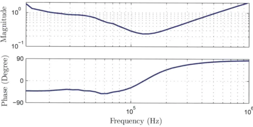
In order to understand the feasibility of this method, it was first important to look at the input impedance of several portable electronic devices in order to understand how their individual input impedances will affect the charging network's total impedance measurement. The input impedances of several mobile electronic devices are depicted in figures 2-4, 2-5, and 2-6. The method of collecting the data for these plots is detailed in appendix B. One can see through these plots the potential for a high frequency measurement of the resistance of the load line cables of the charging network to be distorted by the effective input impedance of a connected device.
1) 0 10... 10 90 90 10 5 10 6 fRequency (Hz)
Figure 2-4: Input impedance of iPad 3G (ID - 2A, VUSB = 5.03V).
The easiest frequency at which to observe the input resistance of the connected device is at the input impedance's resonant frequency because at this frequency the effective series combination of the inductor and capacitor looks like a short circuit. The effective input resistance at the resonant frequency is large for each device rel-ative to the expected resistance of the load line cables. This is an issue because the measurement should only infer the voltage drop over the load line cables and this requires the input resistance of the connected device to look small. If the effective
C) $-10 1 0. . . . . . . . . . . . . .. 1U on 0 5... 10 Frequency (Hz) 106
Figure 2-5: Input impedance of iPhone 5G (ID= 990mA, VUSB= 5.19V).
10 10-90 0 C) CJ2 105 Frequency (Hz) 6 10
Figure 2-6: Input impedance of iPod Nano 3G (ID= 340mA, VUSB= 5.13V).
input resistance of the device is too large, the error in the measurement of the voltage drop inferred over the load line cables will be too large.
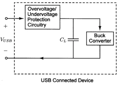
There are several factors that contribute to this effective input resistance. Figure 2-7 shows a more accurate schematic of the input impedance of a connected device. First, there is contact resistance between the USB port and the internal circuitry of the connected device. This contact resistance varies probabilistically from connection to connection, but was measured on average to be 1OOmQ in the iPod Nano 3G. Second, many mobile electronic devices that rely on USB charging have protection circuitry
... - - ! - I - - ! -... ... . .. .. . .. .. .. ... ... .. .. .. ... ... .. .. .. .. ... .. . .. .. ... .. .. . .. .. . .. .. .. ... ... .. . .. ... .. .. ... .. ... .. . .. .. .. .. . . . .. ... .. .. .. ... ..... . .. .. . . . .. .. .. .. . .. .. .. ... .. ... .. .. .. ... ... .. .. .. . WU -V
between their input ports and the charging circuitry. This protection circuitry adds impedance to the current path within the connected device. On top of the protection circuitry, internal parasitic resistances that vary with frequency, such as ESR from the load capacitor, also contribute to the measured input resistance. A measurement of the input resistance can be extracted from an impedance measurement at values away from the resonant frequency of the device's internal impedance, but constant resistances, series resistance from the protection circuitry, and frequency dependent parasitics will affect the impedance measurements at other frequencies as well.
Overvoltage/ Undervoltage 0-4-10 Protection + Circuitry Buck VUSB CL Converter
USB Connected Device
Figure 2-7: Block diagram of connected device's input impedance.
2.2.2 Effect of Device Input Resistance on Voltage
Regula-tion
The voltage this technique is regulating the voltage at the USB port, not the voltage at the load capacitor. The load capacitor, however, is the decoupling capacitor in the frequency measurement, and this means that any input resistance seen between the input terminals of the connected device and the load capacitor will be included in the measurement of the load line resistance. At the same time, table 1.1 shows the resistance of the connecting cables, R, will be between 66mQ and 333mQ, which is of the same magnitude as the input resistances of the connected devices depicted
in figures 2-4, 2-5, and 2-6. The measurement depicted in figure 2-3 will measure the resistance of the line to be R
+
Rist where Ri2 t is the internal resistance of theconnected device, and so the voltage at the USB port, VUSB, will be regulated to
VReg. + ID Rint.
/AVerror _DRt (2.5)
VReg- B VReg.
On top of this error, any of the parasitics that contribute to the total internal re-sistance of the connected device are frequency dependent, however, the measurement is meant to quantify the DC resistance of the load line cables. The measured internal resistance will not precisely equal the internal resistance of the connected device when the DC voltage and current are supplied. This will further distort the measurement of the load line resistance.
The direct impedance measurement technique is compatible with systems where a decoupling capacitor can be placed exactly at the point at which one wants to regulate the voltage. These systems should draw minimal current and have negligible parasitic impedance over the network whoes voltage drop is to be compensated, compared to the DC impedance of the network.
2.3
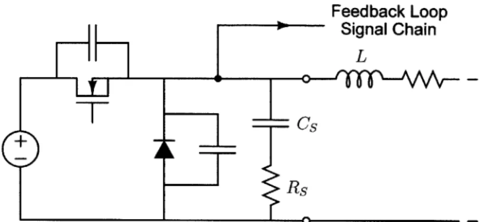
Method C: Current Interrupt Measurement
t=0 R L
VI N - Vt L ID
VIN-IT I
L---i USB Connection Figure 2-8: Circuit implementation of method C.
The third technique, method C, is labeled the "Current Interrupt Method" be-cause it stops the flow of current into the charging network in order to bring the
voltage drop over the load lines to OV, and then samples the voltage stored over the load capacitor as an approximation of the voltage at the USB port.
The implementation of method C is depicted in figure 2-8. The voltage source,
VIN, models the power supply, the resistance, R, and inductance, L, model the load lines, and the load capacitance, CL, and current source in parallel, ID, model the connected device. In this method, a switch separates the power supply and the load lines, and a protection diode with forward voltage, VD, bridges the two input terminals of the load line network.
2.3.1
Analytical Solution of Method C
i (t) Vm(t) ICL(t) v(t1),v(t2) = iL(t) 0 t 0 -t t1 t2 At
Figure 2-9: Plots depicting method C including the current delivered to the connected device and the measurement voltage waveform.
Initially the switch is closed and the current path is from VIN, through the con-necting load lines and into the current source of the connected device. The voltage over CL equals the voltage at the USB port, VUSB, which is the voltage that should be regulated to VReg.. After the switch is opened at time t = 0, the current through the
connecting load lines, iL(t), will ramp down to OA, as shown in figure 2-9. Meanwhile, the current supplied by the load capacitor to the current source in the connected de-vice, ic, (t), will ramp up until it is supplying the entire load current, ID. The voltage over the diode during this time frame is depicted in figure 2-9. After a time period of At there is no current through the diode and connecting load lines and the voltage drop over the connecting load lines will equal OV. The voltage over the diode will equal the voltage over the load capacitor and so is sampled at time, t,. This sampled
voltage equals VUSB minus the voltage dissipated from the load capacitor as a result of supplying power to the current source between the moment when the switch was opened and the sampling time.
VUSB V(tm) j t C
(tm)+ I tm - for tm > At (2.6)
CL ( 2
Equation 2.6 shows that the voltage sampled over the diode at time, tm, is equal to
VUSB minus the error term that comes from the load capacitor being discharged. Fig-ure 2-9 shows that in the case where two points are sampled, (ti, v(ti)) and (t2, v(t2)),
an estimate of the voltage over the load capacitor before the "current interrupt" switch was opened can be calculated to further reduce the error in the inferred USB voltage,
VUSB,1-v(t1) -v(t2) ID
VUSB,1 = - tl v(tl) = VUSB + At (2-7)
The time it takes for the current in the load lines to fall to OA, At, is derived in appendix A.
At = (2.8)
VD + IDR +VUSB
If VUSB, from equation 2.7 is assumed to be the voltage at the USB port in steady state, then the feedback loop will servo to the point at which VReg. = VUSB,1. Sub-stituting equation 2.8 into equation 2.7, and solving for this servo point gives the steady-state voltage at the USB port as a function of circuit parameters.
(VReg. - VD -- DR) + (VReg.+VD + IDR 2 _ IDL
VUSB 2 2 2CL (2.9)
From (2.9), JAVerror/VReg.13 is plotted in figure (2-8).
Method C is most compatible with systems of minimal current and load line cable inductance, with a relatively larger load capacitor. Method C has the undesirable effect of strong EMI generation because of the "current interrupt" feature. Method
C is compared to methods A and B in section 2.4.
2.4
Comparison of Virtual Sense Techniques for
Automotive USB Buck Application
In order to determine which of the previous three techniques is most appropriate for regulating an automotive USB buck converter, it is necessary to observe the derived errors in voltage regulation within the application space detailed in table 1.1.
The only variable that can be adjusted when implementing method A, in order to minimize the error in the voltage at the USB port generated by the technique, is the frequency of operation. The error is minimized when the technique's frequency of operation is maximized. As indicated in table 1.1, the maximum frequency of operation considered is 400kHz.
The only variable the applications engineer has control over in implementing method B is the frequency that the impedance analyzer operates at. Unfortunately, this is of little use because there are parasitic impedances at all frequencies of op-eration that will affect the impedance measurement. The errors of method A and method C will both become exacerbated by the effective DC internal resistance be-tween the USB port and the load capacitor, however, method B also suffers from the parasitic resistances that come into play, and that are difficult to define, by using a high frequency measurement.
If one was trying to implement method B to charge the iPad, for example, one would observe this issue. The iPad's effective input impedance measured at resonance is 0.25Q. Assuming VReg. = 5V, there would be a 0.5V error at the USB port if the
technique were implemented, which corresponds to 10% error. It will become evident that method A and method Cs' errors can be reduced significantly below this.
Method A and method Cs' errors are definable and practical to mitigate, whereas method B's error will vary widely between devices. For these reasons, method B was not chosen as the technique to be implemented.
The only variable that can be adjusted when implementing method C is the for-ward voltage of the diode, VD. Figure 2-10 compares the regulation error using method
A and the regulation error using method C. In each case, ID= 2A, and VReg. = 5V.
Method A is assumed to be operating at 400kHz. Method C is assuming the diode's forward voltage is 0.4V. A 3m, 20AWG twisted pair cable was wound and its induc-tance, L, was found to be 1.6pH. This value was used in the calculation of method B's error. While the error from each method is comparable, the error from method C is shown to be less than the error from method A for the entire range of load capacitors in consideration. Method C was therefore chosen as the technique to be implemented for the automobile's virtual sense voltage regulation loop.
0.3 0.25-0.2 \ 0 .1 5 -. . . .. . .-.. . -0.1 -0.05 - -0 1 2 3 4 5 6 7 8 9 10 Load Capacitance (pF) - - - Method A Method C
Figure 2-10: The smallest achievable errors in the worst case scenarios over the range of possible load capacitances for method A and method C.
Chapter 3
Feedback Loop Design for Current
Interrupt Regulation Technique
3.1
The Backwards Projection Algorithm
The current interrupt method is a technique for sensing the voltage at the USB port by which a feedback path can be constructed and regulation can be implemented. Section 2.3.1 showed that if two samples are taken a more accurate sampling of the voltage at the USB port can be calculated.
vctL(t) VC VUSB vCL (t) Slope -ID 2 CL S pSlope =9CL9 VUSB,1 VUSB,2 V(ti) -V(t2) -t 0 t At i ti t2
Figure 3-1: Depiction of algorithm.
The left-hand plot in figure 3-1 shows the voltage over the load capacitor once
the "current interrupt" switch is opened at time, t = 0. During the first time period, At, the voltage over the load capacitor dissipates at the rate ID/(2CL). This is the period during which the current in the load lines is ramping down to OA. Thereafter, the voltage over the load capacitor is being dissipated at the rate, ID/CL.
Two voltage samples can be taken, v(ti) and v(t2), once the current in the load
lines is OA and any transients in the voltage waveform have died out. This corresponds to the period when the voltage over the load capacitor is dissipating at a rate of
ID/CL. The algorithm assumes the slope the voltage over the load capacitor has
been dissipating at up until the first sample was taken, and then calculates what the voltage over the load capacitor was at the moment the switch was opened. Two natural slope assumptions are ID/CL, which corresponds to the first version of the algorithm, and ID/(2CL) which corresponds to the second version of the algorithm. The first version of the algorithm was give by equation 2.7 and is repeated below.
v(ti) - v(t2) ID
VUSB,1 =l +l V(t1 USB 2CLAt (3.1)
The other option for the algorithm assumes the voltage over the load capacitor is decreasing at half the rate assumed in the original technique up until the first voltage is sampled.
_ v(t1) -v(t 2) (ID +ID
VUSB,2 - 2( 1 - 2 1 v(ti) =USB - ti At
2(t1 -t2) 2CL 2CL
Letting t1 = At + t', and t2 = At + t',
VUSB,2 VUSB - D (3.2)
2CL
Versions 1 and 2 of the algorithm are illustrated in the right-hand graph in figure 3-1. Comparing the errors of each algorithm, version 2 will be more accurate when faster time-to-sample speeds are achievable such that t1/2 < At. Furthermore, the
error from using version 2 decreases with faster time-to-sample speeds. Otherwise, version 1 should be used as it maintains a constant error of ID/(2CL)At independent
of the time-to-sample.
3.2
Basic System Architecture
The basic system architecture of the automotive USB power delivery system without feedback regulation consists of the regulation voltage, VIN(s), minus the voltage drop over the load line which can be modeled as a system disturbance, D(s), giving the voltage at the USB port, VUSB(s). This system is depicted in figure 3-1.
D(s)
VIN(S) -0---s' VUSB(S)
Figure 3-2: Basic power delivery system architecture.
The current interrupt method introduced in 2.3 is used to put a feedback loop around the system depicted in 3-1 with the intent of removing the steady-state effect of the voltage drop over the load line cables, D(s), on VUSB(S).
3.3
Feedback Loop
The current interrupt method is implemented through zero-order sample-and-hold circuitry combined with analog circuitry which performs mathematical operations corresponding to the backwards projection algorithm. In the following calculations, version 1 of the algorithm was assumed. The feedback path will therefore consist of a block representing the effect of the current interrupt method and following algorithm calculations on the signal cascaded with a zero-order sample-and-hold block.
3.3.1
Current Interrupt Method Block Model
Equation 2.7 combined with equation 2.8 shows that the current interrupt method infers the voltage at the USB port plus an error term that is a function of the voltage at the USB port.
VFB = VUSB + L(33)
2CL (VD + IDR +VUSB)
where VFB is the output of the current interrupt method's system block. The block diagram representation of the current interrupt method can be approximated by a gain block of magnitude equal to unity plus a constant error term. The error term in equation (3.1) is a non-linear function of VUSB, however, the error term can be
linearized around the steady-state DC operating point of the circuit [9]. Taking E to be the constant error term contributed by the current interrupt method,
I%2L (VD + IDR
+
2VUSB)2CL (VD + IDR + VUSB 2 VUSB
The system block representing the current interrupt method can then be reduced to a gain block of gain (1 + E).
3.3.2
Sample-and-hold System Architecture
The current interrupt method's calculation circuitry requires that the voltage mea-surements be acquired through zero-order sample-and-hold circuitry. If the sampling occurs periodically every T seconds, then the system block representation of the sample-and-hold is,
GsH(s) = (3-5)
S
which is mathematically equivalent to VUSB(t) being sampled at time t nT, and
output from the feedback path as the voltage at the USB port until time t = (n
+
1)Twhere a new voltage sample is taken [5]. The implication of the sample-and-hold block is that the system needs to consider the discrete time system effects. The consequence of this on the system's performance is that the system can become unstable because a delay is introduced in the feedback path in the relaying of information from the output to the control circuitry.
3.4
Control System Architecture
The purpose of the feedback loop is to compensate for the voltage drop over the load line cables, so an integrator needs to be used to compare the regulation voltage and the voltage at the USB port, and then incrementally increase the voltage supplied to the circuit from the power supply at a rate proportional to the error. This strategy ultimately sets the voltage at the USB port equal to the measured voltage from the feedback path, and so the only error between the voltage at the USB port and the regulation voltage will be from the error term inherent from the backwards projection algorithm.
cc
R. Re
Vin (8s) 0- /
-Figure 3-3: Practical circuit implementation of integrator.
Figure 3-2 shows the practical implementation of an integrator op amp circuit. The transfer function of the integrator block, Gi(s), then takes the shape of a low-pass filter.
(s) = Gi(s) = - (3.6)
Vin Ri RcCs + 1
The behavior of the system can be further optimized by cascading a gain block of gain -K with the integrator block giving the compensation block the transfer function G(s) = -KGi(s).
D(s)
VIN(S) - G(s) VUSB(S)
t = nT
Figure 3-4: Voltage regulation control ioop schematic.
3.5
Voltage Regulation Control Loop
3.5.1
Continuous-Time Analysis
The entire control loop can now be assembled and is depicted in figure 3-4. If the sample-and-hold effect on the system is ignored, the system can be approximated as a continuous time system. This corresponds to the sample-and-hold system operating at a high enough frequency such that the delay in the feedback path is negligible. Setting the disturbance equal to zero, the closed-loop transfer function is,
USB =
KR(37)
VIN RiRcCes + Ri + KRe(1+ )
This system is very stable with a single closed-loop pole. The ratio Rc/Ri
>
1 so that the DC error in the loop is made negligible and inherently 1>>
E, therefore, the single pole is approximately located atK
p ~ -- for K < Re/Ri (3.8)
P RiCc
The closed-loop system gain could be adjusted to push the pole outwards and speed the system up. If the system were still too slow, compensation could be added to reduce the phase margin and speed the system up.
3.5.2
Discrete-Time Analysis
The effect of the sample-and-hold block on the closed-loop system needs to be ana-lyzed in order to understand the effect of the frequency of operation of the system,
f,
on the system's behavior. Appendix C shows the derivation of the discrete closed-loop transfer function in terms of z, where z = esT.
VUSB() (RcRi)K(1 - e-T/(RcC))(
VIN z -e T/(Rcc)(1 (Rc/Ri)K(1 + e)) + (Re/Ri)K(1 + e)
A direct consequence of equation 3.9 is that the bottom limit on the operation frequency is given by
1 K
f > ~ assuming RC > Ri and 1> E RCCl n RcK(1+E)+Ri 2RjCe
(RCK(1+f)-RiJ
If the system is operating at a slower frequency, the delay between control decisions
will be too long and the integrator will effectively be over-correcting such that the error each time step is greater than the error from the previous time step. This corresponds to the system being unstable.
The upper bound on the frequency of operation is dependent on the behavior of the voltage over the load capacitor after the "current interrupt" switch is closed. After the switch is closed the load capacitor will charge to its steady state value which will result in an under damped second order step response over the load capacitor as a result of the relative values of the effective series resistance, inductance, and capacitance of the network. The oscillations must die out before the current interrupt method can be repeated. Otherwise, the measurement of the voltage at the USB port will be corrupted by the oscillations. When the switch is closed, the circuit looks like an RLC network with the effective resistance being equivalent to the sum of the load line resistance, R and the effective series resistance of the "current interrupt" MOSFET,
Rsw. The time constant for this network is then 2L/(R + Rsw), and so the voltage
over the load capacitor has settled to within two percent of its final value after a time equal to four times the network's time constant; t = 8L/(R + Rsw). The time
between measurements, T, must therefore be greater than 8L/(R+Rsw)+tu,,, where to, is the time for which the switch is opened and the voltages at the measurement node are being sampled. Generally, t,,
<
8L/(R + Rsw), and so the upper boundon the frequency of operation of the circuit is given.
K(1 + c) (R + Rsw) (3.10)
2RjCe 8L
Equation 3.9 shows that in order to decrease the lower bound on the frequency of operation, the control loop must be slower. Decreasing the gain of the loop, K, achieves this, however, the trade-off is that the DC error between VIN(s) and VUSB
increases. This is because there is a resistor in the inverting feedback path of the integrator op amp that is implemented in order to keep non-ideal DC bias currents from the op amp from saturating the capacitor in the inverting feedback path. It therefore creates a path in the system loop for a DC bias voltage that it inversely proportional to the gain K. Another option for decreasing the lower bound on the frequency of operation is to increase the time constant of the integrator by increasing Ri or Cc. Again, this will cause the system to take longer to settle to its final value. Many portable electronic devices have a small time allowance for perturbations in the voltage at the USB port to settle to the appropriate regulation voltage. If the system response is too slow and these perturbations do not settle out in time, the internal power circuitry of the connected device will shut off in some cases or become damaged in others. The integrator must operate at a sufficient speed so that perturbations settle within this allowed window of settling time.
The upper bound on the frequency of operation of the circuit is mostly dependent on the characteristics of the load line cable used. The inductance and the resistance of the load line cables probably cannot be manipulated for achieving a higher upper bound on the frequency of operation as they are generally predetermined constraints of the application. Increasing the effective resistance of the RLC network when the switch is closed is a method by which one may increase the upper bound on the fre-quency of operation. This can either be achieved by increasing the effective resistance
of the "current interrupt" MOSFET or by adding a resistor in series with the MOS-FET. This will reduce the ringing after the switch closes and allow the switch to open
sooner. This solution is a power inefficient solution because whenever the switch is closed, all the current supplied to the connected device must be pulled through the added resistor, however, more complex mechanisms, such as switching the resistor in and out of the current path at the appropriate times, may alleviate this issue.
3.6
Overview of Feedback Loop Behavior
The feedback loop behaves as a first order DT system. The operation constraints are such that the frequency of operation of the system be between K(1+E)/(2RiCc) <
f
< (R + Rsw)/(8L) for stability and signal integrity purposes. One may adjust theseparameters within the circuit to achieve a higher or lower frequency of operation. Furthermore, one may add lag compensation circuitry to the feedback loop so as to decrease the phase margin and speed up the system even more.
Chapter 4
Implementation of the Current
Interrupt Method
4.1
Considerations for Board Level
Implementa-tion of the Current Interrupt Technique
A board level implementation of the current interrupt method regulating a USB
voltage while charging a portable device was constructed as a proof of concept. Several aspects of this method's implementation needed to be analyzed more thoroughly before a circuit board could be built up.
4.1.1
Device Characteristic Considerations for Power
MOS-FET and Protection Diode
The "current interrupt" switch that will periodically turn off and keep current from being drawn from the power supply into the load line cables will be implemented with a power MOSFET. Both the power MOSFET and the protection diode will have parallel parasitic capacitances that will affect the speed at which the technique can be performed as well as the integrity of the voltage signal at the measurement node.