Publisher’s version / Version de l'éditeur:
2005 Annual Report Conference on Electrical Insulation and Dielectric Phenomena, 2005-10-16
READ THESE TERMS AND CONDITIONS CAREFULLY BEFORE USING THIS WEBSITE. https://nrc-publications.canada.ca/eng/copyright
Vous avez des questions? Nous pouvons vous aider. Pour communiquer directement avec un auteur, consultez la
première page de la revue dans laquelle son article a été publié afin de trouver ses coordonnées. Si vous n’arrivez pas à les repérer, communiquez avec nous à [email protected].
Questions? Contact the NRC Publications Archive team at
[email protected]. If you wish to email the authors directly, please see the first page of the publication for their contact information.
NRC Publications Archive
Archives des publications du CNRC
This publication could be one of several versions: author’s original, accepted manuscript or the publisher’s version. / La version de cette publication peut être l’une des suivantes : la version prépublication de l’auteur, la version acceptée du manuscrit ou la version de l’éditeur.
Access and use of this website and the material on it are subject to the Terms and Conditions set forth at
Nanodielectric Surface Performance When Submitted to Partial Discharges in Compressed Air
Fréchette, M. F.; Larocque, R. Y.; Trudeau, M. L.; Veillette, R.; Cole, K. C.; Ton-That, M.-T.
https://publications-cnrc.canada.ca/fra/droits
L’accès à ce site Web et l’utilisation de son contenu sont assujettis aux conditions présentées dans le site
LISEZ CES CONDITIONS ATTENTIVEMENT AVANT D’UTILISER CE SITE WEB.
NRC Publications Record / Notice d'Archives des publications de CNRC:
https://nrc-publications.canada.ca/eng/view/object/?id=4d45b3c9-1f79-4143-9e85-50de74fa0258 https://publications-cnrc.canada.ca/fra/voir/objet/?id=4d45b3c9-1f79-4143-9e85-50de74fa0258
2005AnnualReport ConferenceonElectrical Insulation and Dielectric Phenomena
Nanodielectric Surface
Performance
When
Submitted
to
Partial
Discharges
in
Compressed
Air
M. F.Frdchette,'R.Y.Larocque,1 M.L.
Trudeau,'
R.Veillette,'
K.C.Cole,2 and M.-T. Ton That2 lInstitut de recherched'Hydro-Quebec2lnstitut des materiaux industriels CNRC Quebec, Canada
Abstract: Bulk samples of a nanodielectric material weresynthesized. Thisinsulatingmaterialconsisted ofa mix of epoxyresin,aSiO2load andapercent fraction of inorganic nanoparticles. The aim of the present experi-ment was to determine theperformance of the nanodi-electric surface when exposed to partial discharges as
compared to that of an epoxy containing only the mi-crometric SiO2 load. A discharge situation featuring a triple-junction condition was used. Low-intensity dis-chargeswereproduced alongagap formedbythe inter-face between compressedair and the bulk sample. The materialcontainingasmallamountofnanoparticleswas
foundto resist much morethe presentdischarge condi-tions, showing an improved performance as compared tothat observed in thecaseof the epoxy without nano-clay.
Introduction
The broadfield of nanoscience has shown signsof con-vergenceatthe turn of the century. Thiswasconsidered to have a great potential for insulating systems and dielectrics. It was put forward then [1] that new and improved dielectrics would be found among the nanos-tructured ceramics and tailored nanocomposites. Nano-dielectrics wereperceivedasemergingas anewclass of materials.
Since then, the trend showinganincrease inactivity has beenmaintained (see for instance [24]), the various effortsproducingadiversifiedwide spectrum of results, and thehope that this would elicita momentumtransfer in the field of electrical insulation and dielectric phe-nomenahasquickly materialized. In the past few years, the number ofpublished scientific contributions in this particular domain has increased considerably. For in-stance, atthe CEIDP2005 alone and for the second year inarow, there will be about 20 papers dealingmore or less with nanodielectrics [5]. One of the key points of the recentyears, in the field of nanoscience or specifi-callyfor thenanodielectrics,has been therecognition of the need for amultidisciplinary approach and the suc-cess of implementing it. Past experience permits to speculate that the time counter is running fast for the field to produce some breakthroughs in order to keep
could betofind and achieve aprofitable electrotechni-calapplication.
The present contribution looks at an extrapolated situation dealing with anexistinginsulating material. It is rather revolution from the inside that is sought. For high-voltage applications, epoxy is often used with a high-percentload ofsilica. The silica load is sometimes of crystalline nature or could be, but the size of the particles ranges mostly in the micrometric scale al-though it is observedto be distributed in values some-times reachingdownto nanometers [6]. Adown-sizing of the crystals into the nanometric scale and its adjunct tothe epoxy could inprinciple improvetheperformance of the material. In addition, the percent-load could be reduced considerably as it was observed in many in-stancesthatasmallquantity of nano-additives brings a substantial change. In this effect, it is contended that surfaceareaassociated with the nanoparticles isa lead-ing parameter. But here a different approach is fol-lowed. The question is rather how a current system, a two-phase bulk consisting of dispersed particles in a polymericmatrix,canbeaffected by addingtoit nanos-tructures. Wouldtheperformance of it be affected, im-proved andto what extent? How does the nanometric additive interact with suchatwo-body system?
In this work, a comparative study was conducted seeking to establish the relative surface resistance to partial discharges of two insulating material systems. The referential systemwasprepared consisting of epoxy with ahigh-content silica load. A similar system con-tainingin addition asmall amountof nanoclays consti-tuted the nanodielectric. The experimental conditions are essentially those corresponding to low-intensity discharge interactions with dielectric surfaces for which exposurecanbemaintainedovertime.
Experimental context
Material preparation
Thereferencedielectric material consisted of micromet-ric silica dispersed in an epoxy matrix at a loading of 60% by weight. The epoxy resin consisted of a com-mon resin based on DGEBA (diglycidyl ether of
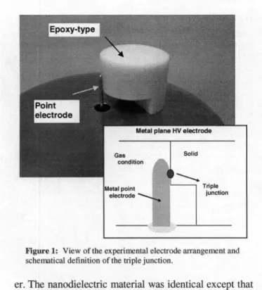
Figure
1: View of the experimental electrode arrangemnentandscheniaticaldefinition of thetriplejunction.
er.The nanodielectric material was identical except that a commercially available nanoclay (a layered silicate treated with organic intercalant) was well dispersed in the epoxyresin before it was mixed with hardener and silica and cured. The amount ofnanoclay was chosen so that the content of nanometric silicate in the final product corresponded to 0.45% of the total weight, or 1.1%of theepoxymatrix weight. When such nanoclays are fully welldispersed, they give rise to silicate plate-lets with athickness of about1 nm and a diameter in the range of 100-500 nm. Cylindrical bulk rods were molded in plastic containers. The thus obtained surfaces were used as such in the experiment. However, the cylinders were tailored to the proper dimensions and cleaned for grease and moisture.
Experiment
A detailed description of this type of experiment was providedovertheyears [7-10], asit formsabasic con-text for discharge interactions with an insulating sur-face. A discharge situation featuring a triple-junction condition was used. Low-intensity discharges were produced along a gap formed by theinterface between compressed air and the bulk sample. A plane/point/ plane electrode configuration was used. Alongside the point electrode that extended from one of the planes, was the solid bulksurface. The gap length was consti-tuted by the interface between the gas medium and the solid material surface. The distance between the point electrode andopposed planeamounted to5 mm.Figure 1 illustrates the experimental arrangement. The gas pressure was fixed at 5 bars. AC voltage was applied
andavoltage-value givingreasonable discharge activity was set. Attimes, this applied valuewasre-adjusted to maintain the discharge activity. Discharge characteris-ticsweremonitoredusinganICCDcameraandanICM. Voltage was applied overextended periods of time, in a continuous or uncontinuous manner, giving atotal ex-posuretime.
Discharge conditions
One of the elementsof importance from thestandpoint of the experiment was to succeed in controlling the appliedstresses tothe surface understudy. The basis of the experiment is toknow what type ofstresses is ap-plied to the surface. Then, to be able to reproduce and control these stresses overtime isanessential in sucha comparative study.
Much effort has been devoted to establish a con-trolled-discharge environment. Knowledge of the dis-charge situation was clarified. A fibre-optic intensified charge-coupled display detector (FOICCD)with a spec-tral response between 200 and 600 nm was focusedon theareaof interest.The camera aims atthe point elec-trode through a sapphire window. The camera is an ICCD type with a possible gain up to 106, witha fast response (amaxof 1 Msample/s) and is UV enhanced. Inaddition, theincoming lightwent through a telephoto (5X) equipped withquartzlenses.Typically, the camera was operated in a continuous mode and opened gate with again set at 150 (maxbeing 255). The 16-bit pre-amplified signal is transmitted via a high-speed serial cabletoa dedicated computervia a FO interface. Over a time frameduring 100 ms, light wasintegrated and the resulting image recorded. Figure 2 shows anICCD
rec-kctive
area
Figure2: Localization of the light activity observed during the discharge exposure.
728
400 350 300 250 >- 200 150 100 50 0 0 20 40 60 80 100 nthf..
Figure3: Measured light intensity (Y in a.u.) as a function of consecutive ICCDtime frames (nth).
ording of the light that corresponds to a time frame of 100 ms. In the background, in light shade, are featured the epoxy-type bulk and the electrode profile. The use of AC voltage, as opposed to DC voltage, produces a discharge locatedatthe triple junction,which is clearly shown in Fig. 2. Evidence presented in Fig. 3 estab-lishes that the discharge emits almost continuously. In this graph,light intensity in arbitrary unitwasdisplayed as afunction of the consecutively recordedICCD time frame. The darker symbols are ascribed to the back-ground noise.
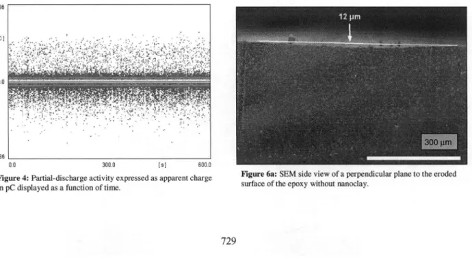
Insuch an electrodeconfiguration, the voltage span between corona threshold and breakdown is usually narrow. The applied voltage value was set as to get the partial-dischargepattern asexemplifiedinFig. 4. Figure 4featuresanICMrecordingin which thepeak charge is displayed as afunction of time. Typically, rates exceed-ing 25 negative-pulse counts per second with peaks larger than 5 pC were encountered.
Material
characterization
The case ofepoxy without nanoclay was processed first.
.186
-186
Figure5: Viewofthenanodielectric surface after discharge expo-suretakenwith anopticalmicroscope.
The duration of discharge exposure amounted to 13.5 hours. Surface conditions were inspected periodically. At this time, erosion of the surface was apparent. This fixed the reference time line for the exposure duration to be applied totheepoxy containing nanoclay. After the same discharge duration, no apparent surface degrada-tion was observed. Exposure continuedtoreach a total duration of 25 hours. Then, the bulk was removed and its surface imaged using a depth-of-field compensated optical microscope.
As canbe seenin Fig. 5,minimal damage occurred and the original marks associated with the mould are
still visible. On the contrary, the surface of the
two-body epoxy, thus without clay, showed a substantial damaged area: An oval shape measuringabout500
g.m
by 1400gm.
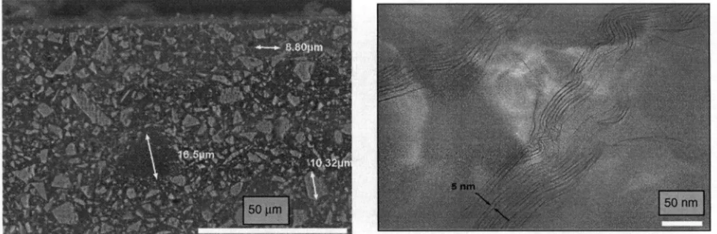
Variousmicroscopy techniqueswereused tocharacterize the materialmicrostructureand to further investigate this greatresistance exhibited by the epoxy containing nanoclay.The bulk without clay having the eroded surface was cut perpendicularly to its surface with adiamond
Figure 6a: SEM sideview ofaperpendicular planetothe eroded
surface of theepoxywithout nanoclay.
AnEa
..g]
Izi A
1 ; ;
U--
-0.0 308.0 [IS 00.0
Figure4:Partial-discharge activity expressed as apparent charge in pC displayed as a function of time.
Figure6b: SEMmicrographofaperpendicular cut of theeroded
surface; Epoxy without nanoclay and sideviewwithanangle.
blade. This gave access to the side view of the valley associated with the surface degradation. Observation made with a scanning electron microscope (variable-pressure SEM, 50 Pa) is presented in Fig. 6a where a
12-gim
lowering is found atthe apexof thedegradation valley. Further enlargementasshowninFig. 6b, againa side view but with anangle this time, permits to image and distinguish the microstructure. Whitish structures below the surface are silica particles. Their nature has been confirmed by running X-ray scattering. They are distributed in size. Ithas been shown [6] that nanomet-ric silica particles (a few) can exist. But the majority is in themicrometric range. The darker areas seen inFig. 6a are the organic epoxy matrix. They reflect less and appear darker. Again it was confirmed that in such a situation the larger micrometric particles at the surface or close to it offer the greater resistance to discharges[6].
What is happening with the 2-body epoxy contain-ing nanoclay? What brings the improved performance? The above analysis was applied to the nanostructured epoxy.The SEMmicrograph presentedinFig.7ashows a side view of the sliced bulk. Thecut was
perpendicu-Figure 7b: TEM micrograph of the epoxy containing nanoclay. Grouping of the well dispersed platelets into the epoxy matrix.
lar to the discharge-exposed surface. As in the former case, observations are very similar exceptfor the pres-ence now of dark rounded structures having approxi-matecircular diameter oftens of microns. X-rays scat-tering performed on these structures indicates the pres-ence of alumino-silicates (with traces of iron). There-fore, these are not blobs ofpolymers. These could be associated withamodification of the fabricationprocess due to the agglomerated presence ofnanostructures or be an artifact ofsynthesis since the material (and its process) is notoptimized. Analysis was pushed further byusingatransmission electronmicroscope.Thinslices having a surfaceof 30
gim
X30jimand thickness of 80 nm wereobtained from the sideplane shown inFig. 7a using ultramicrotomy. Many of these slices were ana-lyzed by TEM. Two examples are provided in Figs. 7b and 7c. Figure 7b is a typical image of the situation: Nanometric structures have appeared in-between mi-crometric silica. Typically, the nanostructures are notfoundclose to the micrometric particles oraggregates.
Figure7a:SEMmicrograph showingaside view of the epoxy bulk with nanoclay.
Figure 7c: TEM micrograph ofthe epoxy containing nanoclay
showing the well dispersed platelets ofalumino-silicates.
They standalone inthe matrix.Having longerextension (as longas400nm)than width(inthe range of 50to80 nm), they show some structure. These results from the well-achieved dispersion of the nanoclay. Figure 7c presents anenlargedview of thedispersedplatelets.The valueof 5 mmwould tendtoindicate someexfoliation, asit exceeds natural inter-cavern distances.However, it is not a measureof the exfoliationstatus of the bulk. It would appear that theadjunct of nanometric inclusions multipliesthe number ofbonds andchangesthebonding naturewith the surroundings.
Closing
remarks
Electrotechnical applications make use already of 2-phase epoxy. The present contribution has sought to investigate if adding a small amount of nanometric additives to an existing recipe could revolutionize its performance. In the context, it was found that the ad-junct resulted ina substantial improvement of the sur-face performance resisting to degrading effects associ-atedwith partial discharges. The welldispersedplatelets were foundtogroupinto the epoxy matrix andnot ob-served to interact with the micrometric silica. It gives the image ofligamentary re-enforcement of the weak medium,i.e. the epoxymatrix. The resultslook promis-ing with the reserve that the material is not optimized andthatthepropertiesmaydepend muchonthe synthe-sis process[11-12].
Acknowledgment
The authors wouldliketothank G. Belanger, theformer Dpt. Manager of Chimie et materiaux at IREQ for al-lowing this collaboration and encouraging efforts in this research area. RecentfinancialsupportfromHQ Strate-gicStudies isacknowledged.
References
[1]M.F.Frechette, M. Trudeau, H.D.Alamdari,andS. Boily:
"Intro-ductory Remarks on NanoDielectrics," Proc. EEE Conference on
Electrical Insulation and Dielectric Phenomena, Kitchener, Ontario,
Canada, Oct. 14-17 (2001). Anextended versionhas beenarchived subsequentlyinIEEETrans. on Diel. and Electr, Insul., Vol. 11,No.
5,pp.808-818 (2004).
[2] FirstInternational SymposiumonNanostructured and Functional Polymer-based Materials and Nanocomposites, April 24-27 2005,
Dresden, Germany.
[3] InternationalConferenceonNanomaterials and Nanotechnologies (NN2005), Crete, Greece;June14-18,2005.
[4] Polymer nanocomposites 2003, International conference heldat BouchervilleCanadaandorganized bytheIndustrial Material Institute CNRC, 6-8 October 2003. There will be Polymer nanocomposites
2005thisyear,scheduled28-30 September.
[5] CEIDPstandsforConferenceonElectrical Insulation and
Dielec-tric Phenomena. The 2005 annual meeting was held in Octoberin
Nashville, Tennessee. The 2004 version was inBoulder, Colorado. Seethe website:http://ewh.ieee.org/soc/dei/ceidp/
[6]M.F.Frechette, R.Y.Larocque, R. Veillette,andM.L. Trudeau:
"Mesoand nanomorphologicalchanges ofanepoxysurfaceexposed
tolow-intensitydischarges in air", IEEE Conf.onElectrical Insulation
andDielectric Phenomena,Boulder, Colorado, USA, October 17-20 (2004).
[7] M.F.Frechette,R.Y.Larocque, C. Hudon, T. Umemura, S.
Ma-tsumoto and T. Takahashi, "Corona discharge phenomenology at onset in weakly electronegative gas miixtures," Proceedings Ninth International Symposium on Gaseous Dielectrics, Baltimore USA, May 21-25, 2001.
[8]M.F.Frechette and R.Y. Larocque, "Partial discharge behaviorat the interface between solid and gaseous insulation," International SymposiumonElectrical Insulation, Boston, USA,pp.395-398,Avril
2002.
[9]T.Takahashi,M.F.Frechette,R.Y.Larocque, C. Hudon, T.
Ume-mura, S.Matsumotoand H.Okubo,"Long-termsequential
character-isticsofnegative partialdischargeinpressurizedSF6 gas",
Proceed-ings Ninth International SymposiumonGaseous Dielectrics, Balti-moreUSA, May 21-25, 2001.
[10]M.F. FrechetteandRendY.Larocque, OpticalEmission
Charac-teristicsofaTriple Junction IEEE ConferenceonElectrical Insulation
andDielectricPhenomena, Boulder, CO USA,Oct.17-20 2004 [11] Michel F. Frechette, "Reflectingonmaterialtrends:thecaseof nanodielectrics", Proceedings of the 35th Symposium on electrical andelectronicinsulating materials and applicationsin systems, pp.
25-32,Tokyo, Japan, Novembre17and 18, 2004.
[12]S.S.Ray andM.Okamoto: "Polymer/layeredsilicate
nanocom-posites:areviewfrompreparationtoprocessing",Progress in Poly-merScience, Vol. 28,pp.1539-1641 (2003)
Author address: Michel Fr6chette, IREQ, 1800 boul. Lionel-Boulet, Varennes, Qc, Canada, J3X