Open Archive TOULOUSE Archive Ouverte (OATAO)
OATAO is an open access repository that collects the work of Toulouse researchers and
makes it freely available over the web where possible.
This is an author-deposited version published in :
http://oatao.univ-toulouse.fr/
Eprints ID : 12280
To link to this article :
DOI:10.7567/JJAP.53.08MC03
URL :
http://dx.doi.org/10.7567/JJAP.53.08MC03
To cite this version :
Reig, Benjamin and Bardinal, Véronique and Doucet, Jean-Baptiste
and Daran, Emmanuelle and Camps, Thierry and Aufray, Maëlenn and
Lamure, Alain and Tendero, Claire Study of SU-8 reliability in wet
thermal ambient for application to polymer micro-optics on VCSELs.
(2014) Japanese Journal of Applied Physics, vol. 53 (n° 8S2).
08MC03-1-08MC03-5. ISSN 0021-4922
Any correspondance concerning this service should be sent to the repository
administrator:
[email protected]
Study of SU-8 reliability in wet thermal ambient for application
to polymer micro-optics on VCSELs
Benjamin Reig1,2, Véronique Bardinal1,2*, Jean-Baptiste Doucet1,2, Emmanuelle Daran1,2,
Thierry Camps1,3, Maëlenn Aufray4, Alain Lamure4, and Claire Tendero4 1CNRS, LAAS, F-31400 Toulouse, France
2University of Toulouse, LAAS, F-31400 Toulouse, France 3University of Toulouse, UPS, LAAS, F-31400 Toulouse, France 4University of Toulouse, UPS/CNRS/INPT, F-31030 Toulouse, France
E-mail: [email protected]
We present experimental data on the reliability of SU-8 polymer when used as a core material for the integration of microlenses on vertical-cavity surface-emitting lasers (VCSELs). The respective effects of a hot and humid environment on structural, mechanical and optical properties of this epoxy resist are investigated. High aspect-ratio SU-8 micropillars are found to keep a good surface morphology and a stable optical transmission, as well as a good adherence on the wafer. Thermal cycling is also studied to check material stability under electro-thermal actuation in SU-8 micro-opto-electro-mechanical system (MOEMS). These results are of great importance for the collective integration of low-cost SU-8-based passive or active microlens arrays onto VCSELs wafers for optical interconnects and optical sensing applications.
1. Introduction
Beam shaping is one of the key issues for vertical-cavity surface-emitting lasers (VCSELs) integration in highly-miniaturized optical systems and for coupling them to single-mode optical fibers.1–4) It is indeed mandatory to associate these laser devices to micro-optical elements to meet most of systems requirements on beam divergence reduction or on beam focusing.5) Early reports on micro-optics association to VCSELs were mainly based on hybrid assembly methods. Nonetheless, these methods require tricky alignment steps and are often not compatible with high density VCSELs arrays. Direct integration of microlenses inside the devices or at their surface was therefore showed to be more efficient and more collective.6,7) In particular, polymer-based technologies using SU-8 material at VCSEL surface were proven to lead to simple and low temperature fabrication process.8–12)SU-8 is a negative-tone epoxy resist that wasfirst used for MEMS molding and for microfluidics fabrication because it allows for high aspect-ratio patterning at a micrometric scale.13)This key feature constitutes a great advantage for the precise fabrication of thick transparent pedestals and of associated microlens necessary for VCSEL beam collimation [Fig. 1(a)]11) or for fabricating optical MEMS for dynamic focusing [Fig. 1(b)].14) One important condition for the future industrial use of such lensed-VCSELs consists in checking reliability in presence of moisture, as it is done for bare VCSELs.15–17) In particular, the stability of optical transmission and adherence of SU-8 on the semiconductor wafer has to be verified.
SU-8 series resist reliability was already investigated for MEMS applications. This resist was first found to be independent to humidity, provided its polymerization process is fully completed.18) However, Ali et al. reported that absorption of water in the material can lead to swelling and to a residual strain in SU-8 cantilevers.19)This phenomenon was also observed by Feng et al. who assumed a reversible mechanism.20) These authors concluded that the resulting strain can be minimized by applying a drying process. Park et al. led an extensive reliability study on silicon-based
MEMS including SU-8 spacers (made of SU-8-2000).21) Their actuators were submitted to mechanical stresses (shocks and vibrations), to hot and humid storage conditions and to thermal cycling. Storage at 85 °C with a relative humidity (RH) of 85% was found to cause SU-8 delaminat-ing at a level that depends on the resist version and on storage duration. Finally, Salm et al. highlighted sensitivity of SU-8 to humid environments (30 °C, 95% RH), reporting a decrease of SU-8 adherence on CMOS chips.22) However, to our knowledge, there is no data available for the last version of the resist for which the formulation was improved in terms of adherence (SU-8 3000 series). Moreover, only few studies were led on SU-8 reliability over long storage durations and none of them considered the dimensions involved for VCSELs beam shaping, neither the evolution of optical properties after aging. To this end, we investigate here
(a) (b) (d) VCSEL VCSEL SU-8 pedestal SU-8 MEMS anchor microlens microlens (c)
Fig. 1. (Color online) Principle of operation (left) and corresponding scanning electron microscope (SEM) images (right) of two different types of SU-based microlenses collectively integrated on VCSELs by the authors: (a, b) cylindrical pillars for static collimation; (c, d) optical MEMS with rectangular anchors for dynamic focusing.
the evolution of structural, mechanical and optical properties of 100-µm-thick SU-8 micro-optical structures submitted to hot and humid environment and to thermal cycling.
2. Experimental methods
To carry out this study, accelerated aging tests were performed using a climatic chamber in which temperature and humidity levels could be real-time controlled with reduced transient times (Vötsch VCL 0010). Thanks to an experimental Taguchi plan,23) it was possible to lead a comprehensive study including three parameters at three different values (temperature: 33, 50, and 85 °C, RH level: 50, 65, and 85% and duration: 100, 500, and 1000 h) while reducing the number of tests conditions (from 27 to 9). As seen in Fig. 2, the most severe conditions were: 85 °C, 95% relative humidity and 500 h, which are the typical aging conditions to check optoelectronic devices reliability forfiber optic telecommunications.
A batch of 10 samples, corresponding to the reference state and to the 9 different aging conditions, was prepared. We have used 4 in. silicon wafers with a thin silicon dioxide layer (thickness³2.5 µm) deposited at the surface by low temper-ature plasma enhanced chemical vapor deposition (PECVD), in order to reproduce well the surface of a SiO2-passivated VCSEL wafer, onto which we usually integrate our SU-8 static11) or tunable12) lens, the thermal properties of GaAs and Si wafers being very close. A similar batch was also fabricated on transparent substrates (Corning Pyrex 7740) and simultaneously aged, to make possible optical trans-mission measurements. A 100-µm-thick SU-8 layer (SU-8 3050 Microchem™) was deposited on each wafer by standard spin-coating. Cylindrical patterns corresponding to microlens pedestals were then defined with diameters ¤ equal to 50, 100, and 200 µm using photolithography (Fig. 3). A standard hard-bake (2 min at 125 °C) was performed to make sure that complete polymerization was reached. 500-µm-length rectangular patterns with widthsW equal to 50, 80, and 100 µm were also included to make possible mechanical tests (shear-tests) on patterns corresponding to lens pedestals and to MOEMS anchors. After fabrication, the samples were successively placed at the center of the climatic chamber. They were then systematically characterized two days after the end of the aging test.
3. Results and discussion 3.1 Surface characterization
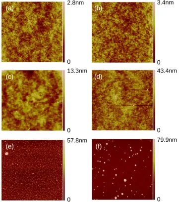
SU-8 surface profile was characterized before and after each aging process using an atomic force microscope (AFM; Bruker Dimension 3100). Two areas of 5© 5 = 25 µm2were scanned for each considered pattern. As seen on images measured after aging No. 7 and No. 9 (Fig. 4), nano-sized bubbles appear randomly at the surface. The origin of these bubbles is not clearly stated. As bubbles distribution is found to systematically vary with the substrate type (silicon or Pyrex), it could be correlated to the large difference of
Fig. 2. (Color online) Aging test matrix.
(d)
(b)
(c)
(a)
Fig. 3. (Color online) Top: Description of the SU-8 microstructures fabricated on SiO2/silicon to reproduce the passivatived surface of a VCSEL
wafer (a) and on Pyrex for optical transmission measurements (b). Bottom: SEM images of SU-8 cylindrical (c) and rectangular (d) patterns designed for aging tests. (b) (a) (e) 2.8nm 3.4nm 79.9nm 57.8nm 0 0 0 43.4nm (f) (d) 0 0 (c) 13.3nm 0
Fig. 4. (Color online) AFM images of SU-8 surface (5© 5 µm2): Initial
state: (a) on silicon (b) on Pyrex. After aging No. 7: (c) on silicon (d) on Pyrex. After aging No. 9: (e) on silicon (f ) on Pyrex.
thermal properties between the two kinds of substrates (for example their thermal conductivities: respectively 149 and 1.1 W m¹1K¹1) leading to a difference of thermal transients during baking steps on a hot plate. In both cases anyway, bubbles size and density increase with simultaneous increase of temperature and humidity levels, with maximal diameters than can reach locally 60 nm for silicon and 80 nm for Pyrex for the most drastic test (aging No. 9: 85 °C, 95% RH, and 500 h). However, it is worth noting that the corresponding average surface roughness remains in all conditions lower than 4 nm (RMS), as seen in Table I. These values remain acceptable for the aimed application.
3.2 Optical characterizations
Optical transmission spectra of SU-8 micro-patterns in the visible-NIR spectral range (600–1100 nm) were measured thanks to a FTIR spectrometer equipped with a microscope stage (spatial resolution ³20 µm). Whatever the considered aging test, the variation of polymer transmission was found to be smaller than the measurement error of the set-up used (1%). As seen in Fig. 5 for the case of aging No. 9, SU-8 transmission remains higher than 98% in the VCSEL operation wavelength range, i.e., around 850 nm. Moreover, we have checked that no significant optical diffusion could be
measured in the structures despite the presence of the nano-bubbles at the surface.
Finally, to evaluate water absorption in SU-8 material, we also measured its absorption spectrum in the MIR spectral range (from 4000 to 600 cm¹1) using attenuated total reflexion (ATR). The ratio of the peaks areas measured respectively in the 3686–3621 cm¹1region (corresponding to O–H bonds) and in the 3500–2766 cm¹1region (correspond-ing to C–H bonds) has been compared before and after ag(correspond-ing test. We noticed a significant increase of this ratio just after aging: from 1.13 to 2.2 for the highest humidity level. However, it returns rapidly to 1.6 after a short storage in ambient air (less than one day) and to 1.3 after two days in a nitrogen storage box. These results demonstrate that water absorption in SU-8 due to exposition to wet ambient is largely reversible.
3.3 Mechanical characterizations
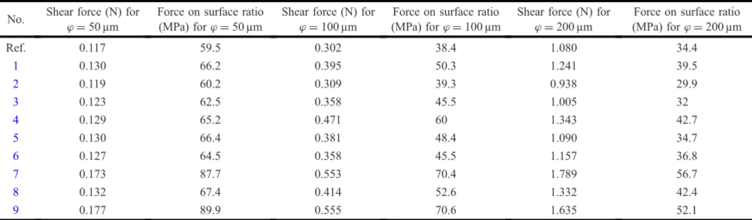
Two adherence tests were used in order to characterize the SU-8/SiO2assembly. First, mechanical peeling experiments were performed to measure the propagation of a crack at the interface.24) An Instron 3367 machine was used at 10 mm/min, and 90° for 1 © 8 cm2 bands of SU-8. These measurements showed that SU-8 exhibit a very good adherence on SiO2: an average minimal peeling force of 6.8 N/cm was indeed obtained; this value being only limited by the used set-up. Secondly, initiation tests were performed as shear-tests on micro-scale patterns. The principle is based on the measurement of the pressure applied to a blade for leading to a lateral delamination of the microstructure [Fig. 6(a)]. Adherence forces values extracted from these measurements are reported in Table II for small cylinders and in Table III for larger rectangular patterns. As seen in Fig. 6(b), the annular footprint of the released cylinders is clearly visible at the surface, showing that SU-8 adheres more at the pillar periphery than at the rest of the surface. As the ratio periphery-on-surface evolves as 1/R (R being the radius), this bounding effect linked to the periphery is more preponderant in the case of small diameters. We divided the force by the total surface to highlight this size effect (Tables II and III) and to estimate the mechanical shear stress (in MPa). We obtained a higher value for small cylinders (diameter 50 µm) than for larger patterns. In all cases anyway, a value at least higher than 20 MPa was obtained, showing a good stability of the SU-8/SiO2 mechanical interface. Results are even better after long, hot and humid aging tests.
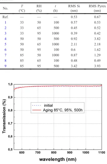
Table I. Average surface roughness (RMS) measured on the reference and after each aging test for samples fabricated on silicon and on Pyrex substrates. No. T (°C) RH (%) t (h) RMS Si (nm) RMS Pyrex (nm) Ref. — — — 0.53 0.67 1 33 50 100 0.57 0.53 2 33 65 500 0.45 0.52 3 33 95 1000 0.39 0.42 4 50 50 500 0.92 3.82 5 50 65 1000 2.11 2.18 6 50 95 100 0.6 1.62 7 85 50 1000 0.87 1.29 8 85 65 100 0.48 0.49 9 85 95 500 3.42 3.93
Fig. 5. (Color online) Transmission spectrum measured on a 100-µm-diameter SU-8 pillar on Pyrex before and after aging test No. 9.
substrate SU-8 Shear-Test blade SiO2 (a) (b)
Fig. 6. (Color online) (a) Principle of shear test measurement. (b) Cylindrical structures before and after peeling.
This tends to indicate that there is an incomplete polymer-ization of the samples at the reference state. Data from mechanical tests were exploited for the analysis of the aging
test matrix (Fig. 7). This study indicates that the most influent factor on adherence evolution is the temperature whatever the considered size, the impact of the others factors variation
Table II. Results of shear-test measurements performed before and after aging on SU-8 cylindrical microstructures fabricated on SiO2/Si.
No. Shear force (N) for ¤ = 50 µm
Force on surface ratio (MPa) for¤ = 50 µm
Shear force (N) for ¤ = 100 µm
Force on surface ratio (MPa) for¤ = 100 µm
Shear force (N) for ¤ = 200 µm
Force on surface ratio (MPa) for¤ = 200 µm Ref. 0.117 59.5 0.302 38.4 1.080 34.4 1 0.130 66.2 0.395 50.3 1.241 39.5 2 0.119 60.2 0.309 39.3 0.938 29.9 3 0.123 62.5 0.358 45.5 1.005 32 4 0.129 65.2 0.471 60 1.343 42.7 5 0.130 66.4 0.381 48.4 1.090 34.7 6 0.127 64.5 0.358 45.5 1.157 36.8 7 0.173 87.7 0.553 70.4 1.789 56.7 8 0.132 67.4 0.414 52.6 1.332 42.4 9 0.177 89.9 0.555 70.6 1.635 52.1
Table III. Results of shear-test measurements performed before and after aging on SU-8 rectangular microstructures fabricated on SiO2/Si.
No. Shear force (N) for W = 50 µm
Force on surface ratio (MPa) forW = 50 µm
Shear force (N) for W = 80 µm
Force on surface ratio (MPa) forW = 80 µm
Shear force (N) for W = 100 µm
Force on surface ratio (MPa) forW = 100 µm Ref. 0.976 39 1.512 37.8 1.666 33.3 1 0.736 29.4 1.431 35.8 1.431 28.6 2 0.849 33.9 1.253 31.3 1.483 29.7 3 0.535 21.4 1.127 28.2 1.563 31.3 4 0.800 32 1.350 33.7 1.797 35.9 5 0.861 34.5 1.402 35 1.732 34.6 6 0.734 29.4 1.116 27.9 1.394 27.9 7 1.131 45.2 1.964 49.1 2.495 49.9 8 0.757 30.3 1.308 32.7 1.718 34.3 9 1.113 44.5 1.758 43.9 2.162 43.2 (a) (b) (c)
Fig. 7. Taguchi plan analysis: evolution of shear stress in function of aging parameters for cylindrical microstructures: (a)¤ = 50 µm, (b) ¤ = 80 µm, and (c)¤ = 100 µm.
(RH% and time) being much lower and we account it to an incomplete polymerization at the reference state.
To further explore temperature individual influence, we submitted new samples to positive thermal cycling tests in normal humidity conditions (40%RH). The following thermal steps were applied: 10 min at 20 °C, ramp up to 120 °C at+10 °C/min, 10 min at 120 °C and finally decrease at ¹10 °C/min down to 20 °C for a total cycle duration of 40 min. The maximal temperature chosen here is higher than 85 °C and corresponds to the operation conditions of the electro-thermal MOEMS we recently developed for tunable lens integration on VCSELs.10,12) The surface structure in this case was found to be close to the one of the reference state (roughness<0.5 nm), confirming that bubbles size and density mainly increase when humidity and heat levels simultaneously increase. Series of 10, 50, and 100 cycles were performed and their respective effect on mechanical shear stress was analyzed. In all these cases, we observed a similar behavior than previously: shear stress remains higher than 20 MPa and increases with tests duration, with a maximum value of 45 MPa for 100 cycles, demonstrating that SU-8 microstructures tolerate well positive thermal cycling.
4. Conclusions
We have studied the reliability of SU-8 polymer as a functional material for the fabrication of integrated micro-optical elements on VCSELs, thanks to aging tests performed in a hot and wet ambient. When increasing temperature and moisture, polymer morphology is found to slightly degrade, with the progressive apparition of “nano-bubbles” at the surface. However, the average surface roughness measured by atomic force microscopy (AFM) remains low: less than 4 nm for the worst case (85 °C, 95%RH, 500 h). Optical transmission measured at VCSEL emission wavelength was also checked and found to be not significantly changed. Besides, the analysis of optical absorption in the mid infra-red range shows that water absorption occurring in the material is largely reversible. Finally, adherence strength of SU-8 on the substrate was also studied. It is found to be high, with measured shear stresses at least equal to 20 MPa. Due to periphery effects, this adherence stress is even twice higher for patterns dimensions lower than 100 µm, that correspond to those involved in typical lens pedestals or MOEMS anchors that we have recently integrated on VCSELs devices. This study also highlighted a higher sensitivity of adherence evolution to temperature than to humidity level or to test duration. Finally, positive thermal cycling tests performed between 20 and 120 °C demonstrate a good mechanical stability of SU8 properties for a use in conditions of electro-thermal actuation. Now that SU-8 microstructures reliability for integrated micro-optics is assessed, our future work will
concern a more complete study of the reliability of lensed-VCSELs devices under laser operation.
Acknowledgments
The authors gratefully acknowledge Région Midi Pyrénées for financial support (FIAB-SU8 project) and RENATECH (French Network of Major Technology Centres) within LAAS-CNRS for technological support. The authors would also like to thank FIABLAB for their contribution to mechanical measurements and Airbus Defense and Space for fruitful discussions.
1) K. Iga,Jpn. J. Appl. Phys.47, 1 (2008).
2) A. Larsson,IEEE J. Sel. Top. Quantum Electron.17, 1552 (2011).
3) R. Michalzik,VCSELs: A Research Review (Springer, Berlin, 2013) Springer Series in Optical Sciences, Vol. 166, p. 3.
4) A. Kroner, I. Kardosh, F. Rinaldi, and R. Michalzik,Electron. Lett.42, 93 (2006).
5) V. Bardinal, T. Camps, B. Reig, D. Barat, E. Daran, and J. B. Doucet,Adv. Opt. Technol.2011, 609643 (2011).
6) Z. Wang, Y. Ning, Y. Zhang, J. Shi, X. Zhang, L. Zhang, W. Wang, D. Liu, Y. Hu, H. Cong, L. Qin, Y. Liu, and L. Wang,Opt. Express18, 23900 (2010).
7) K. S. Chang, Y. M. Song, and Y. T. Lee,IEEE Photonics Technol. Lett.18, 121 (2006).
8) M. T. Gale, C. Gimkiewicz, S. Obi, M. Schnieper, J. Söchtig, H. Thiele, and S. Westenhöfer,Opt. Lasers Eng.43, 373 (2005).
9) A. Nallani, T. Chen, J.-B. Lee, D. Hayes, and D. Wallace,Proc. SPIE5836, 116 (2005).
10) A. Gracias, N. Tokranova, and J. Castracane,Proc. SPIE6899, 68990J (2008).
11) V. Bardinal, B. Reig, T. Camps, C. Levallois, E. Daran, C. Vergnenègre, T. Leïchlé, G. Almuneau, and J.-B. Doucet,IEEE Photonics Technol. Lett.22, 1592 (2010).
12) B. Reig, T. Camps, V. Bardinal, D. Bourrier, E. Daran, J. B. Doucet, J. Launay, and J. Y. Fourniols,J. Micromech. Microeng.22, 065006 (2012).
13) H. Lorenz, M. Despont, N. Fahrni, J. Brugger, P. Vettiger, and P. Renaud,
Sens. Actuators A64, 33 (1998).
14) V. Bardinal, T. Camps, B. Reig, J.-B. Doucet, S. Abada, and E. Daran,Inter. Conf. Optical MEMS and Nanophotonics (OMN), 2013, p. 47.
15) S. Xie, R. W. Herrick, D. Chamberlin, S. J. Rosner, S. McHugo, G. Girolami, M. Mayonte, K. Seongsin, and W. Widjaja,J. Lightwave Technol. 21, 1013 (2003).
16) E. Bosman, J. Missinne, B. Van Hoe, G. Van Steenberge, S. Kalathimekkad, J. Van Erps, I. Milenkov, K. Panajotov, T. Van Gijseghem, P. Dubruel, H. Thienpont, and P. Daele,IEEE J. Sel. Top. Quantum Electron.17, 617 (2011).
17) R. W. Herrick, A. Dafinca, P. Farthouat, A. A. Grillo, S. J. McMahon, and A. R. Weidberg,IEEE J. Quantum Electron.49, 1045 (2013).
18) J. Hsieh, C.-J. Weng, H.-L. Yin, H.-H. Lin, and H.-Y. Chou,Microsyst. Technol.11, 429 (2005).
19) S. M. Ali, S. C. Mantell, and E. K. Longmire,IEEE Sensors, 2008, p. 152.
20) R. Feng and R. J. Farris,J. Micromech. Microeng.13, 80 (2003).
21) J. Park and D.-S. Shin,Mater. Chem. Phys.98, 309 (2006).
22) C. Salm, V. M. Blanco Carballo, J. Melai, and J. Schmitz,Microelectron. Reliab.48, 1139 (2008).
23) G. Taguchi,IEEE Trans. Reliab.44, 225 (1995).
24) T. Nguyen, W. E. Byrd, D. Alshed, J. Chin, C. Clerici, and J. Martin,