HAL Id: hal-02334052
https://hal.archives-ouvertes.fr/hal-02334052
Submitted on 25 Oct 2019HAL is a multi-disciplinary open access
archive for the deposit and dissemination of sci-entific research documents, whether they are pub-lished or not. The documents may come from teaching and research institutions in France or abroad, or from public or private research centers.
L’archive ouverte pluridisciplinaire HAL, est destinée au dépôt et à la diffusion de documents scientifiques de niveau recherche, publiés ou non, émanant des établissements d’enseignement et de recherche français ou étrangers, des laboratoires publics ou privés.
Synthesis and optimization of low-pressure chemical
vapor deposition-silicon nitride coatings deposited from
SiHCl3 and NH3
Benjamin Cossou, Sylvain Jacques, Guillaume Couégnat, Sean King, Liyi Li,
William Lanford, Gyanendra Bhattarai, Michelle Paquette, Georges Chollon
To cite this version:
Benjamin Cossou, Sylvain Jacques, Guillaume Couégnat, Sean King, Liyi Li, et al.. Synthesis and optimization of low-pressure chemical vapor deposition-silicon nitride coatings deposited from SiHCl3 and NH3. Thin Solid Films, Elsevier, 2019, 681, pp.47-57. �10.1016/j.tsf.2019.04.045�. �hal-02334052�
Available at: https://doi.org/10.1016/j.tsf.2019.04.045
Synthesis and optimization of low-pressure chemical vapor deposition-silicon nitride coatings deposited from SiHCl3 and NH3
B. Cossou1, S. Jacques1, G. Couégnat1, S.W. King2, L. Li2, W.A. Lanford3, G. Bhattarai4, M. Paquette4, G. Chollon1*
1Laboratoire de Composites Thermostructuraux, CNRS, 33600 Pessac, France 2Logic Technology Development, Intel Corporation, Hillsboro, OR 97124, USA 3Department of Physics, University at Albany, Albany, NY 12222, USA
4Department of Physics and Astronomy, University of Missouri-Kansas City, Kansas City, MO
64110, USA
*Corresponding author
Abstract
Stoichiometric silicon nitride films were deposited by low-pressure chemical vapor deposition from the SiHCl3-NH3-H2-Ar system in a hot wall reactor at pressures ranging from 0.3 to 2 kPa.
The films are amorphous for deposition temperatures up to 1000 °C and crystalline, in the α-form, at 1200 °C and above. A method for evaluating the internal stresses based on the curvature of the silicon substrate wafer and the resulting silicon Raman peak shift was developed. Some amorphous films exhibit high internal tensile stresses that can lead to cracking during deposition depending on the mechanism and effective precursors involved. Residual stresses can thus be reduced and cracking avoided by, in descending order of importance, reducing the concentration of reactive gases through dilution, increasing the deposition temperature and decreasing the total pressure. The effects of these parameters on the intrinsic stresses were related to the amount of residual hydrogen successively incorporated and thermally released during the growth of the coating according to the Noskov’s model.
Thin films of amorphous silicon nitride (a-SiNx) are widely used in numerous fields, for
instance as passivation and stabilization layers in semiconductor devices [1], or as parts of micromechanical sensors. These applications require high-purity and precisely controlled physical properties, but they also impose processing constraints. Amongst others, the deposition temperature has to be the lowest as possible to preserve the substrate. Thermally-activated low-pressure chemical vapor deposition (LPCVD, here shorten as CVD) is one of the commonly used processes to deposit silicon nitride films. Low temperature CVD requires a highly reactive silicon precursor such as silane SiH4 [2] or dichlorosilane SiH2Cl2 [3], and a nitrogen source,
almost always ammonia NH3.
Silicon nitride (Si3N4) is a ceramic of interest also for higher temperature applications, mostly
for its high resistance against corrosion by liquid metals or metalloids. It is a promising material as a protective layer, e.g. on refractory crucibles for ingot silicon growth [4–6], or on the fiber reinforcement in ceramic matrix composites [7,8]. In this case, the main relevant properties are the chemical and structural stability and the preservation of mechanical properties at high temperatures. The Si3N4 coatings are then deposited at high temperatures (>>1000 °C)
generally using a less-reactive silicon precursor than for semiconductors, e.g. tetrachlorosilane SiCl4. These conditions allow the formation of the crystalline α-Si3N4 phase.
The use of trichlorosilane SiHCl3 as an alternative silicon precursor for the deposition of silicon
nitride has not been much documented yet. This species is expected to have an intermediate reactivity between that of SiCl4 and SiH2Cl2 [9]. It appears as a promising precursor since it
allows the deposition of amorphous silicon nitride at moderate temperatures [10]. It should then lead to the formation of the α phase at temperatures that are necessarily higher but still compatible with sensitive substrates such as fine-diameter SiC fibers. For these reasons, we have used a SiHCl3-NH3-H2-Ar mixture to deposit CVD-silicon nitride films in the present
study.
Whatever the precursor used, a major concern has been pointed out about the growth of the a-SiNx films: cracking due to intrinsic tensile stresses. The key-parameters that were reported to
modulate stress in previous experimental works were the nitrogen to silicon precursor ratio N/Siprec [2,11–14], the deposition temperature T [2,11–13,15] and the total pressure P [2,12,15]. Since too low N/Siprec values may strongly affect the stoichiometry of the resulting film [14], only P and T have been varied in this work, while keeping a high N/Siprec ratio. To get a better thermal stability of the deposited Si-N ceramic, the priority has been given to a Si3N4-like final
structure of the films, i.e. excluding co-deposited free silicon [13]. The aim is then to correlate the tentative deposition mechanisms to the residual stress level in the different films.
2 Experiments and methods
2.1 Deposition and gas phase characterization
The CVD coatings were deposited on substrates of two different types: (100) silicon wafers (10x10 mm x 500 µm) and dense and polished polycrystalline graphite cylinders (10×10 mm). The coated specimens were suspended in the hot zone of a low pressure hot-wall reactor (Fig. 1). The deposition chamber was a vertical silica tube (100 mm in diameter) surrounded by a graphite susceptor heated by radio-frequency induction. The regulation temperature was controlled with a K-type thermocouple installed in the graphite susceptor wall. The temperature profile and the temperature in the hot zone were calibrated by translating a thin additional K-type thermocouple along the reactor axis, at a constant regulation temperature and under a 50/50 vol. % H2/N2 gas flow. This second thermocouple was inserted in a free graphite cylinder
similar to those used for the kinetic measurements to better appraise the substrate temperature. The reactive zone, where most of the thermally activated reactions are expected to occur, was 100 mm long (ΔT < 25 °C). The substrates were placed at the center of this zone, within a 20 mm-length (ΔT < 4 °C). A rotary-vane vacuum pump was connected to evacuate gases at the outlet of the CVD device. The reactor was equipped with systems controlling accurately the temperature T (≤ 1050 °C), the total pressure P (with a motorized valve coupled with a Baratron® pressure gauge, both from MKS) and the various gas flow rates Qi (mass flow meters
from Brooks Instruments) of the precursor mixture (SiHCl3 99 mol% from Sigma Aldrich and
H2 99.9995 mol%, Ar 99.999 mol% and NH3 99.96 mol%, from Air Liquide).
In the standard configuration with steady CVD condition (Fig. 1), a perforated graphite sole was installed at the center of the chamber and the silicon wafer substrates were placed on the sole. The NH3 injection point position was set at 185 mm from the sole, corresponding to a
temperature of ~ 600 °C when the substrates are heated at 1000 °C. The cooling stage of the reactor was natural and, except the initial dwell temperature, identical for all the coatings. Moreover, due to the hot wall configuration, the temperature was very homogeneous through the specimen during cooling. Cracking was therefore not expected to occur due to thermal gradients in the specimen during cooling.
For the kinetic study, the sole was removed and the top of the reactor was connected to a high sensitivity microbalance (from Setaram), to which the cylindrical graphite substrates was hung, allowing the acquisition of the weight gain in the hot zone of the reactor. The deposition rate R (in mg.cm−2.s−1) was determined under stable T, P and Qi conditions and only when a steady
state regime was attained (when the surface state of the coating remains constant versus time). In these conditions, the standard deviation of R calculated from the linear regression of the weight gain versus time raised up to 4% in the worst case in terms of microbalance sensitivity, i.e. at the lowest T and P tested. It was generally much lower (e.g. only 0.1% at 900°C and 2kPa). A series of kinetic measurements (e.g. lnR = f(1/T) or lnR = f(lnQi)) was acquired during a single run with the same graphite substrate, by accumulating different coatings deposited in different conditions. The change in the coating roughness -and thus of the surface area of the substrate- between the beginning and the end of the run may result in some deviations in the R values. In the most unfavorable case, i.e. at high temperature when the surface area (or roughness) can change the most (see section 3), the deviation in the R values can reach up to 20%.
A Fourier transform infrared (FTIR) spectrometer (Nicolet iS50, from ThermoFisher) was coupled to the CVD reactor (Fig. 1). The ex situ detection of the reactants and by-product species and the quantitative analysis of the gaseous mixture were both performed in the transmission mode. The exhaust gases were collected at the outlet of the reactor, cooled down to room temperature and forced to pass through the analysis chamber connected to the pumping system. The incident IR beam was driven axially through the two ZnSe windows of the gas cell (L = 550 mm), before reaching the HgCdTe (MCTA) detector. A constant nitrogen flow was maintained along the beam path outside the gas cell in order to avoid H2O and CO2 absorption.
A specific NH4Cl dust trap (JR TECH) was introduced in the reactor exhaust line upstream
from the IR analysis chamber to prevent powder accumulation on the ZnSe windows and protect the pumping system.
Another high temperature CVD reactor was occasionally used for deposition temperatures ranging from 1200 °C to 1400 °C. It consisted of a graphite tube (instead of a silica tube) of an inner diameter of 40 mm, which is directly heated in its central part by the induction coil. In this case the hot zone was also considered to be 100 mm long, since thermic profiles where almost the same between the two reactors at a maximum temperature of 1000 °C. For the
HT-CVD experiments, the total gas flow rate was adjusted to maintain the same residence time (r)
as for the first reactor.
The conditions used for the different CVD experiments explored more specifically for the coating characterizations are given in Table 1. The deposition temperature T, the total pressure P and the dilution ratio DR = (QH2+QAr)/(QSiHCl3+QNH3) were varied while the
P(NH3)/P(SiHCl3) ratio was kept equal to 5.
2.2 Coating characterization
2.2.1 Measurement of the residual internal stresses by Raman microspectroscopy
The stresses existing in a thin film are often measured from the curvature of the wafer on which the film has been deposited [16]. When the coating tends to densify in situ or after deposition (e.g. due to thermal annealing), it is subject to tension while the substrate underneath is in compression. This effect leads to a measurable curvature of the bilayer that can be measured and directly related to the stress level in the films [17]. This technique is not applicable to all the samples of the present work because it requires that each film be deposited on a large enough silicon wafer substrate, typically beyond 50 mm in diameter. Furthermore, some of the coatings are cracked, which means that the stresses have relaxed at least partially so that the wafer tends to recover its original shape. A technique that is both local and sufficiently accurate to measure residual stresses between cracks is therefore necessary in this case.
Raman spectroscopy is capable of meeting this need. The stress intensity can be easily measured in the monocrystalline cubic silicon substrate from the analysis of the triply degenerated T2g
phonon. When the coating is transparent, such is the case here, the stress due to the coating/substrate mismatch can be measured in the substrate by this technique and compared with data deduced from analytical or finite element modelling [18,19]. In practice, the silicon crystal deformation results in a frequency shift –accompanied sometimes by a broadening– of the original Raman peak due to the anharmonicity of the lattice vibration [20,21]. The shift in frequency depends on the stress state and the Raman diffusion configuration: an equal shift of the triply degenerate modes –without splitting– is observed in case of a hydrostatic stress whereas a splitting between the singlet and doublet components can occur for a uniaxial, biaxial or more complex stress state [20,21]. In the current configuration, i.e. in back-scattering from a (001) face of silicon, with the incident laser beam polarized parallel to the [100] direction and
no polarizer in the scattered beam path, only one (longitudinal optic) component is Raman active and expected to shift due to stress [21]. As expected, no significant peak broadening was detected in this case. The global peak shift was assessed by adjusting a Lorentzian function to determine the stresses level. A shift towards higher frequencies indicates that the silicon is in compression. The extent of the peak shift is proportional to the stress level in the wafer. For example, in the same configuration as above and for a uniaxial stress along the [100] crystallographic direction, a 1 cm-1 shift corresponds to a stress of about 434 MPa [20,21]. On the other hand, in the case of an equi-biaxial stress (which is supposed to apply to the current system), only half of this value (≈ 217 MPa/cm-1) is expected [21].
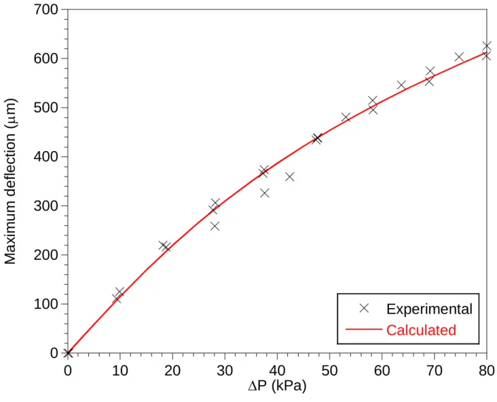
In order to perform accurate stress measurements, a calibrating procedure was proposed consisting in applying exactly the same stress state as that in the coated substrates (i.e. a plane biaxial stress), but to a non-coated silicon wafer. The applied stress intensity was controlled by means of a specific device consisting of a 60 mm x 60 mm perforated metal plate surmounted by a Viton® ISO KF 25 O-ring with a nominal diameter of 40 mm (Fig. 2). A silicon wafer (from Neyco), 50.8 mm in diameter and 500 µm in thickness, was laid on the O-ring. A pressure difference (P=P0-P) was created between both sides of the wafer by means of a vacuum pump
connected to the plate hole. The pressure P was controlled with a capacitance vacuum gauge (133.3 kPa range, Baratron® from MKS Instruments) fitted between the plate and the pump. The pressure difference P and thus the stress applied to the wafer, was adjusted through a fine regulating valve. To compensate the deformation of the O-ring, the maximum deflection of the wafer was deduced by difference between the positions of the center and the edges (under the O-ring), as measured with the fine focus knob scale of an optical microscope (with a x50 objective).
The Timoshenko's model for a uniformly loaded circular plate is usually employed to correlate the pressure difference P applied with the system with the maximum flexural stress σsup at the
surface of the wafer [22]. This model is restrictive as the material is supposed to be isotropic and the maximum deflection not more than one-half the thickness. These assumptions being clearly not valid in the current case, a more realistic model was considered, based on a finite element (FE) analysis. The silicon wafer was simulated using a three-dimensional shell model considering the orthotropic elastic properties of silicon (as reviewed by Hopcroft et al. in [23]), as well as the geometric non-linearity due to large deflections. The wafer (of thickness h) was assumed to be subjected to a uniform pressure P and simply supported at the boundary between the wafer and the DN 25 ISO-KF O-ring (of radius a). The values measured for a and
h were respectively 2.20x10⁻² m and 4.75x10⁻⁴ m. A good agreement was found between the
calculated and experimental maximum deflection wsup of the wafer over the whole range of P
tested (Fig. 3). The maximum stress in the center of the wafer sup for given a value of P was then deduced from the FE model.
The Raman analyses were performed with a Labram HR (Jobin Yvon) microspectrometer (λ = 632.8 nm, spectral resolution ≈2 cm−1
) in the punctual mode (lateral resolution ≈1 μm) at various P values. The corresponding maximum stress was evaluated using the FE model. The evolution of the Raman shift as a function of sup is given in Figure 4.The data are relatively scattered due essentially to the repeatability of the measurements of the silicon peak shift for a given stress state. The relative error in the measurement of P and thus in the calculated value of sup is indeed negligible in comparison. In the experimental conditions employed, the uncertainty of the peak shift was of about +/-0.05 cm-1. The Raman shift/stress slope of 0.00310
± 0.00007 cm-1/MPa (316 ± 7 MPa/cm-1) obtained is surprisingly higher compared with the value found by De Wolf for a biaxial stress state [21]. Yet, for consistency with our experimental procedure, our estimated ratio was employed for the further stress measurements. The final step was to determine the stress level in the thin film itself. The stress assessment is possible by using an extension of the Stoney’s formula [24]. For the current system consisting of a thin coating in tension on a curved thick substrate, Romain-Latu showed that the Stoney’s formula between the maximum stress in the substrate σsmax and the stress in the thin film σc are
linked by Eq. 4, where hc and hs are the coating and substrate thicknesses respectively [25].
(4) 𝜎smax = −3ℎc
ℎs𝜎c
The uncertainty in the value of σc is as high as about 1 GPa due to the variability of the Raman
measurements (due in part to the surface state of the coating), the inaccuracy of stress/Raman shift ratio (see above), and more especially the low hc/hs ratio (2.10-3). This technique is
therefore only applicable in the present case to particularly high stress levels approaching those that can lead to the film cracking, as will be shown below.
2.2.2 Other physico-chemical and mechanical characterizations
The morphology of the free surface of the coatings was observed by scanning electron microscopy (SEM, FEI, Quanta-400 FEG) either in the secondary electrons (SE) or back-scattered electrons (BSE) detection modes. The thickness of all coatings deposited on silicon wafers (e) was evaluated by SEM from fractured cross sections. A dedicated sample was
cleaved before the SEM observations for that purpose.The e values given are averages of 10 measurements along the cross section, the error being around 0.2 m for all coatings. EPMA and ellipsometry were occasionally used to confirm the e values as determined by SEM. These two techniques being indirect measurements (deduced through models), SEM analyses were preferred.
The elemental composition of the coatings was assessed by electron probe microanalysis (EPMA, SC100, CAMECA) at typically 10 kV and 20 nA. The characteristic X-rays were analyzed with WDS spectrometers equipped with LPET (Si) and PC1 (N, O) crystals. Si3N4
and SiO2 standards were used to determine the Si, N, and O weight concentrations. Analyses
were performed in a few cases at various accelerating voltages (5, 10 and 15 kV) to validate the coating thicknesses measured by SEM.
The atomic concentration profiles of some of the films were also recorded by combined nuclear reaction analysis (NRA) and Rutherford backscattering (RBS) measurements. This analysis has been described in detail in another work [26]. The H content was determined using the 15N nuclear reaction method and the N and O concentration from deuteron nuclear reactions. The Si content was measured by 2 MeV 4He RBS. Given the determined H, N, O, Si composition
of the films, parameter-free simulations of the full RBS spectra were performed using the program RUMP [26]. These simulations were then compared to the data to provide a powerful check on the analysis. Films densities in g/cm3 were determined by multiplying the elemental
contents by the masses of these elements, summing over all the elements present (to yield the areal density in g/cm2) and dividing by the film thickness (as measured by SEM and
ellipsometry).
X-ray diffraction (XRD, Siemens D5000, λCu–Kα = 0.1542 nm, functioning in the θ–θ
configuration) was used to detect the presence of crystalline phases in the coatings.
An FTIR spectrometer (Nicolet iS10) was used in the reflection mode with an ATR module (SMART iTR diamond) and a DTGS detector, in particular to examine the Si-H and N-H bond characteristic bands.
The refractive index of a few films was determined using a variable angle spectroscopic ellipsometer (J. A. Woollam VASE) [27]. Five different incident angles (55, 60, 65, 70, and 75°) were utilized to collect reflectance in the 600-1000 nm wavelength range where the extinction coefficient for the SiN dielectrics was negligible. The Woollam software was then
used to deduce the thickness and refractive index (RI) as a function of the wavelength. The specific refractive indices for the films are reported at a wavelength of 673 nm.
The elastic modulus (Y) and hardness (H) of approximately 1 micron-thick coatings were determined by nanoindentation using a Berkovich cube corner diamond tip and a Hysitron Triboindenter with a load range up to 4 mN [28]. Each sample was tested at ten different locations. Depth-dependent properties were examined by performing multiple load/unload cycles at different indentation loads. The film modulus was then calculated using the depth-dependent apparent modulus via a linear extrapolation [29].
3 Results
3.1 Kinetic study and gas phase analysis
In a first step, the influence of the deposition temperature was investigated within a large temperature range (650-1050 °C), for a total pressure P of 2 kPa and reactive gas flow rates of QSiHCl3 = 10 sccm and QNH3 =50 sccm, (PNH3/PSiHCl3 = 5). Preliminary experiments showed that
the nature of the dilution gas (either H2 or Ar) have no influence on the deposition kinetics (not
shown). A mixture of QH2 =250 sccm and QAr =250 sccm was added to the reactive gases,
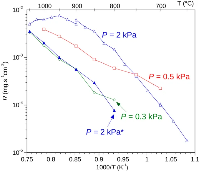
setting a dilution ratio (QH2+QAr)/(QSiHCl3+QNH3) of DR = 8. Three domains can be identified
on the Arrhenius plot of the deposition rate R recorded at P = 2 kPa and DR = 8 (Fig. 5). The first domain below 800 °C, where lnR linearly increases with 1/T, corresponds to a chemical reaction-limited regime (CRR) with an apparent activation energy Ea of 230 kJ.mol-1. The
occurrence of a CRR regime was confirmed by the constant deposition rate observed when varying Qtot for Qtot > 300 sccm, at a given temperature of 750 °C (not shown). Above 800 °C,
R becomes less temperature-dependent. This can be explained by an increasing contribution of mass transfer. At 900 °C, R was indeed found proportional to Qtot. Above 900 °C, the growth
rate is not thermally activated at all, or even slightly decreases when the temperature increases. This feature suggests the occurrence of a pure mass transfer-limited regime accompanied by a depletion of reactive gases near the substrate, due to the upstream deposition on the reactor walls or an early nucleation in the homogeneous phase. The two experimental points presented at 900°C on the P = 2 kPa curve (Fig. 5) illustrate a 20 % deviation of R related to the change in surface roughness (area) of the specimen. In this case the Arrhenius curve was indeed recorded in two distinct runs (for T≤900°C and T≥900°C) with two different substrates (see section 2.1).
The decrease in total pressure from 2 to 0.3 kPa leads to a significant overall decrease of the growth rate (Fig. 5). It also results in a change in the slope of the Arrhenius curve (100 kJ.mol -1 for 0.5 kPa, 160 kJ.mol-1 for 0.3 kPa), possibly attributed to a change in the deposition
mechanism. The increase of the dilution ratio DR from 8 to 18 (QSiHCl3 / QNH3 / QH2 / QAr = 5 /
25 / 250 / 280 sccm) has a similar effect as the pressure decrease. The Arrhenius curve for P = 2.0 kPa and DR = 18 is indeed almost the same as for P = 0.3 kPa and DR = 8 (Fig. 5). The concentration of the reactive species must therefore be regarded as a key parameter influencing the deposition rate and possibly also the nature of the coating (e.g. microcracking). The activation energy obtained in the latter conditions (i.e. at a lower pressure or a higher dilution ratio) is close to the activation energies reported in other works carried out at very low pressure (Ea = 171 kJ.mol-1 at P = 0.07 kPa [10], Ea = 170 kJ.mol-1 at P ≤ 0.133 kPa [30] and Ea = 151
kJ.mol-1 at P = 0.015 kPa [31]), although the precursors used in these cases were SiHCl3 for the
first study and SiH2Cl2 for the two others. A common type of chemical mechanism is likely to
be involved during deposition at such very low supersaturation of the gas phase. It is difficult to compare the Ea values obtained at higher concentrations of reactive species with other data
from the literature because no previous studies conducted in this particular range of conditions have been reported so far.
Although SiH2Cl2 and SiCl4 could be both detected from the decomposition of a simple mixture
of SiHCl3 and H2, no gas products were detected by FTIR from the full initial gas system at the
exhaust of the reactor (at room temperature). Only the presence of NH4Cl condensed on the
ZnSe windows could be noticed as a by-product (Fig. 6). The residual H2O and CO2 absorption
peaks on the IR spectra can be explained by the presence of residual ambient air along the IR beam path, outside the reactor, despite the nitrogen purge. The Si and N precursors, taken separately, remain sometimes present in the gas phase (either SiHCl3 in Figure 6a, when
P(NH3)/P(SiHCl3) < 5, or NH3 in Figure. 6b, when P(NH3)/P(SiHCl3) > 5). Depending on the
initial gas composition, these species are not completely thermally decomposed or consumed through gas phase or gas-solid chemical reactions (e.g. due to deposition in the hot zone or the formation of NH4Cl).
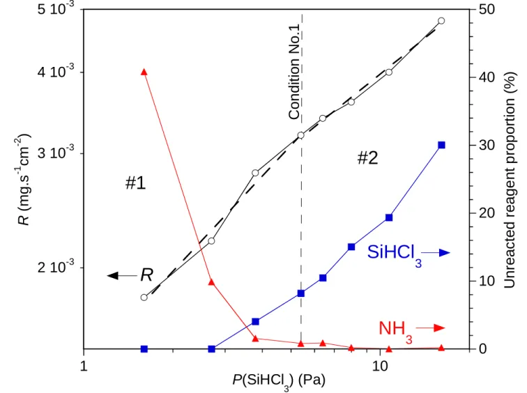
The apparent reaction orders with respect to the initial gaseous reagents were determined starting from the reference condition No. 1 (P = 0.3 kPa, QNH3/QSiHCl3 = 5, DR = 8, see Table
1), by varying one of the partial pressure while keeping the other constant. The total gas flow rate was also kept constant by compensating the variation of the reagent flow with an opposite change of the flow of argon, as a buffer. The reaction order with respect to SiHCl3 is
approximately 0.5 at low SiHCl3 partial pressures (domain #1, QSiHCl3 = 3 - 10 sccm) and 0.4 at
higher partial pressures (domain #2, QSiHCl3 = 10 - 30 sccm) (Fig. 7a). On the other hand, the
NH3 reaction order is about 0.8 at low NH3 partial pressures (domain #3, QNH3 = 10 - 50 sccm)
and almost 0 at high pressures (domain #4, QNH3 = 50 - 200 sccm) (Fig. 7b). For the last high
NH3 pressure domain, the increase in total gas flow rate Qtot was found to lead to an increase in
the growth rate R, indicating a control by mass transfer. In contrast, a chemical reaction-limited regime was obeyed within the three other partial pressure domains.
As long as P(NH3)/P(SiHCl3) < 5, R remains highly dependent on P(NH3) (domain #3). R can
also be increased regardless of the initial amount of NH3 introduced, if a higher proportion of
SiHCl3 is introduced in the system (domain #2). In the latter case, the FTIR analyses show that
NH3 is fully consumed at the reactor outlet. Conversely, SiHCl3 becomes the rate-limiting
species when P(NH3)/P(SiHCl3) > 5. In this case, R indeed decreases with P(SiHCl3) in domain
#1. On the other hand, in the particular case of high NH3 partial pressures, R can still be
increased with P(SiHCl3), provided the total gas flow rate is raised in parallel to prevent the
mass transfer limitation observed in domain #4. When the P(NH3)/P(SiHCl3) ratio is greater
than 5, the limiting reagent SiHCl3 is fully consumed (domains #1 & #4). In domain #4, the
amount of NH3 exceeding this ratio is fully recovered in the gaseous phase at the reactor outlet.
Thus, from the initial flow rate QNH3 of 200 sccm, 100x(200 - 50)/200 = 75% of this species do
not react and leave the reactor after cooling down at room temperature. It is worth noting that in domain #1, the calculation is not accurate due to the small quantities involved and the overlapping of the NH3 IR peaks with those of residual moisture (Fig. 6b). In domains #2 & #3
where P(NH3)/P(SiHCl3) < 5, the excess SiHCl3 is no more found at the reactor outlet, although
the IR peaks are well separated so the peak area can be accurately measured (Fig. 6a). At least a part of the SiHCl3 excess is therefore consumed by the reactions involved during deposition.
The reference conditions No.1 clearly correspond to a transition between different mechanisms controlling the deposition. This phenomenon might result in a variation in the composition of the coating (specifically an excess of silicon when P(NH3)/P(SiHCl3) < 5).
3.2 Coating analysis
The properties of the coatings deposited on (100) silicon wafers, in well-defined steady CVD conditions, are presented in Table 1. The thicknesses as measured by SEM are mostly of the order of 1 m and were found homogeneous along the surface within +/-0.2 m.
As anticipated above, the EPMA results confirm that the coatings produced in domains #2 & #3 are silicon rich, whereas those obtained in domains #1 & #4 have an atomic composition corresponding to Si3N4. More generally, all the deposits synthesized with a P(NH3)/P(SiHCl3)
ratio of 5 (Table 1) are stoichiometric (Si = 42-43 at. %, N = 56-57 at. %, O < 1 at. %) regardless of P, T, DR and the position of the NH3 injection along the reactor axis. The presence of chlorine
is not detected in the coating except very small amounts (just above the detection limit) for P = 2 kPa and T < 1000 °C. In contrast, a deposit obtained at T = 900°C, P = 2 kPa and a P(NH3)/P(SiHCl3) ratio of 3 consists of 47 at. % Si, 49 at. % N, 2 at. % Cl and less than 1 at.
% O (≈9 at. % excess silicon). The refractive index of the coatings (measured at a wavelength of 673 nm), which is closely related to the chemical bonding nature of the films [32,33], was correlated with the elemental composition. The indexes obtained for two films deposited with a common P(NH3)/P(SiHCl3) ratio of 5, but different T and P (condition No. 1: at 1000 °C / 0.3
kPa and condition No. 12: at 800 °C / 1 kPa), were respectively equal to 2.02 and 1.97. These values confirm that the N content is roughly the same in the two coatings and indicative of a high proportion of Si-N bonds and a low H-content. In comparison, the refractive indexes are substantially lower for hydrogenated amorphous silicon nitrides coatings (a-SiNx:H) obtained by plasma-enhanced CVD [34] and higher for silicon-rich coatings obtained by LPCVD [35]. However, silicon-bonded and nitrogen-bonded hydrogen atoms are detected by ATR-IR spectroscopy, especially in the coatings deposited at high pressure (from 1.0 kPa) and low temperature (below 1000 °C). The proportion of Si-H and N-H bonds decreases when T increases at P = 1.0 kPa (Fig. 8). At 1000 °C, the amount of Si-H bonds decreases with P and N-H bonds are hardly detected. The NRA-RBS analyses confirm that a high pressure and a low temperature both promote the incorporation of hydrogen into the deposit. The coating obtained in condition No. 12 (1.0 kPa / 800 °C) indeed contains up to 5.0 at. % hydrogen, whereas the condition No. 1 (0.3 kPa / 1000 °C) leads to a hydrogen concentration of only 0.8 at. %. The interpolation of the NRA-RBS data and the set of ATR-IR analyses (Fig. 8) suggest that the hydrogen concentration increases in the series of coatings deposited at 1000°C, when P increases from 0.3 to 1 kPa (No. 1-4). The densities of the films evaluated for these two conditions were respectively 2.8 and 3.2 g.cm-3. The latter value is close to the theoretical density of crystalline α-silicon nitride (3.17 g.cm-3 [36]) and indicates that the film is pure and dense although amorphous, as will be shown in the following paragraph. The former value, in contrast, suggests that the coating is not fully pure and might involve some residual hydrogen [37].
As evidenced by XRD, the coatings are fully amorphous when deposited at temperatures below 1200 °C, they start to crystallize in the α-form at 1200 °C and they are fully crystalline at 1300 °C or above (Fig. 9). These results are consistent with previous studies from the literature as the formation of α-Si3N4 requires either a higher temperature, using less-reactive precursors
(e.g. 1300 °C using SiCl4 [38]) or a lower temperature, in case of more reactive precursors
(1100 °C using SiH4, [39]). The deposition of crystalline Si3N4 from SiHCl3 / NH3 mixtures
was not reported in previous studies.
The nanohardness, as measured with a Berkovich indentor, is 29.8 GPa for the coating deposited in condition No. 1 whereas it is only 17,9 GPa for the condition No. 12. These results are consistent with the other characterizations of the films. The deposition at high temperature and low pressure (condition No. 1: 0.3kPa / 1000 °C), leading to a pure and dense coating, indeed leads to a higher hardness than the film obtained at a lower temperature and a higher pressure (condition No. 12: 1.0 kPa / 800 °C). The results are also in good agreement with another work reporting a hardness ranging from 23.5 GPa (for an amorphous film deposited at 800 °C) to 33.3 GPa (for a crystalline coating obtained at 1200 °C) [40].
The elastic modulus, also as measured by nanoindentation, is equal to 288 ± 7 GPa for coating No. 1 and 239 ± 9 GPa for coating No. 12. These values are consistent with the high modulus expected for LPCVD materials (280-290 GPa, for coatings deposited at 750 °C-850 °C and 0.04 kPa [41]). Again, the low density material exhibits a lower stiffness than the other coating. As for the density, the presence of a higher residual hydrogen concentration might be responsible for the lower elastic modulus of coating No. 12 [37].
Many of the films deposited on silicon wafer were found partially cracked (Fig. 10b) and even sometimes heavily cracked, especially at P = 2.0 kPa (Fig. 10c). The other coatings, however, still appeared undamaged, especially when the deposition temperature was high, i.e. if T ≥ 1000 °C (Fig. 10a). When they appear, cracks can be easily observed by optical microscopy or even with the naked eye. Coatings of higher thickness were occasionally prepared to study the influence on the cracking pattern. A 25 m-thick coating deposited in condition No. 9 was examined in cross section. After the deposition of a few microns, the coating cracked and flaked during deposition, carrying away small fragments of the substrate (SupMat 1). The rugged surface and the detached fragments were then covered with a new layer of same nature, which subsequently cracked with a more complex pattern. The morphology at low scale shows concave-shaped flakes all along the surface, indicating that the coating shrunk during
deposition. This phenomenon reveals that, at least for condition No. 9, cracking occurred during deposition at high temperature as a result of purely intrinsic stresses due to densification. On the other hand, SEM observations confirmed that the nearly 1 m-thick coatings deposited at 1000 °C do not exhibit cracks at all and have a smooth surface, in particular when the deposition pressure was low (Fig. 11a). If T is lowered below 1000 °C, cracks appear in the films (Fig. 11b) whatever the nature of the substrate (SiO2, SiC, Si, C). Because of the insufficient pumping
capacity, the occurrence of cracks in the coatings could not be verified for P < 0.3 kPa. At a very high temperature (1300 °C) the coating is apparently not cracked, but its surface becomes rough and faceted due to crystallization (Fig. 11c). For T = 1000 °C, an increase of P above 1.0 kPa leads to a rougher surface, making difficult the observation of potential cracks (Fig. 11d). Such a high roughness is attributed to the starting homogeneous phase nucleation. Thus, if P becomes too high (2.0 kPa), the deposit is no more dense and only a white powder of approximate composition Si3N4 is formed in the reactor. These results on the occurrence of film
cracking are summarized in Figure 12.
The influence of the dilution ratio on film cracking can be readily deduced; the reference condition No. 1, with DR = 8, lead to a crack-free coating. Conversely, cracks are observed for the condition No. A2, for which DR was divided by 4 (not shown). This result shows that a decrease in the concentration of reactive species prevents the formation of cracks in the coating. The pressure range leading to crack-free coatings was too narrow to clearly evidence the P effect solely from the occurrence of cracks. The influence of the deposition pressure can be more precisely determined by measuring residual internal stresses with the Raman spectroscopy method (Fig. 4). The stress levels measured in the coatings are reported in Table 1 and ranked in Figure 12. Crack-free films deposited at 1000 °C are not subject to any measurable residual stress for P ≤ 0.5 kPa. Above 0.5 kPa, the coatings undergo an internal tensile stress, which increases with P up to ~5 GPa at P = 1.0 kPa. The internal stresses in the cracked or crystalline films were not reported. Residual stress is indeed expected to be at least partly released due to the cracking process, especially close to the crack edges. Furthermore, the high roughness of the crystalline (conditions No. T1-3) or heavily cracked coatings (conditions No. 10 & 13)
induced artifacts in the Raman spectra leading to inconsistent stress values.
The kinetic study showed that the increase of the deposition temperature essentially enhances the kinetics of heterogeneous reactions in the chemical reaction-controlled regime (Fig. 5). The increase of the total pressure also improves the deposition kinetics through the change of the precursor partial pressures. But P seems also to affect homogeneous reactions, as suggested by the changes in the activation energy of deposition rate. These changes in effective precursors may alter the deposit composition, physical properties and, eventually, stress state.
As concluded in many previous studies [42,43], the cracking of silicon nitride films seems essentially related to the generation of intrinsic stresses rather than thermal stresses. The first major point is that cracks occurred whatever the nature of the substrate (SiO2, SiC, Si, C) for
the coatings deposited at low T. Besides, the thicknesses of all the coatings tested in this study being similar, the occurrence of fracture in the various coatings cannot be associated to hc
exceeding a critical value (for a given a fracture energy and elastic properties of the films and the substrate) [44]. Stresses of a purely thermal origin is unlikely because of the apparently good thermal match of silicon and Si3N4 (e.g. compared to Si and SiO2) [42,43]. The
coefficients of thermal expansion (CTE) reported for various Si-N-(H) films appear relatively scattered [37], but this is due to the variety of processes involved and residual hydrogen contents. Even if measurements have been recently carried-out on Si-rich silicon nitride coatings up to 800K [45], most of the CTE values available for Si3N4 coatings are deduced from
the curvature of Si3N4/Si bilayers at room temperature and supposed to be constant with
temperature. Direct measurements of the longitudinal thermal expansion of free standing Si3N4
coating strips showed that the CTE actually increases significantly with T to get close to that of silicon [43]. The resulting stress in the Si3N4 film is then of only a few hundreds of MPa, i.e.
well below the highest stress levels measured in the current crack-free coatings.
The occurrence of intrinsic stresses and the residual stresses evidenced in the films seem to be related to the amount of residual hydrogen. One of the main conclusions of our work is indeed that cracking, residual stresses and hydrogen content are all the more significant when the deposition pressure P is high and the dilution ratio DR and temperature T are both low.
On the one hand, high partial pressures of reactive species (due either to a high total pressure or a low-dilution) may promote condensation reactions in the homogeneous phase, leading to Si-N intermediates as effective precursors of the deposit [46,47]. These heavy molecules, composed of Si-N bonds or even silazane units, can trap high amounts of residual hydrogen in the solid. These species are indeed formed by the reaction between the initial precursors, which
themselves contain a significant amount of hydrogen. These reactions take place during the gas transport towards the hot zone of the reactor, while the temperature is raised, in a similar way as during the preparation of Si3N4 nanopowders by thermal decomposition of gas precursors
[48,49]. After adsorption on the substrate –provided T is low enough to avoid homogeneous phase nucleation– these heavy silazane species decompose, with the removal of the major part of the hydrogen. The H2 release causes the reorganization and shrinking of the film and
therefore intrinsic stresses according to Noskov's qualitative model [50].
On the other hand, low partial pressures of reactive species limit the possible interactions between SiHCl3 and NH3, leading only to the formation of light chlorinated silanes and/or
silicon subchlorides [51]. These small Si-bearing molecules as well as NH3 or NH3-derived
radicals, adsorb on specific sites at the substrate surface where they can interact with each other. These heterogeneous reactions eventually lead to the formation of the Si-N bonds constituting the silicon nitride deposit. A simple model based on a Freundlich's adsorption isotherm [30] or ab initio calculations [52] can be used to simulate the growth of Si3N4 according to such a
mechanism. The different effective precursors and therefore the different mechanisms involved in the very low pressure deposition result in lower Ea values than the 230 kJ.mol-1 found with
P = 2.0 kPa and DR = 8. Although there must be less hydrogen trapped in coatings grown from the light effective precursors, cracking can still develop if the temperature is too low (i.e. T < 1000 °C). At a given temperature, because of the lower amount of residual hydrogen and therefore the limited shrinkage, the crack pattern appearing is less dense (Fig. 10b) than at higher pressure (for which heavy silazane species are presumably formed) (Fig. 10c). The use of low pressures also allows increasing the deposition temperature above 1000 °C to obtain dense α-Si3N4 films without homogeneous phase nucleation. In these conditions, SiHCl3 tends
to decompose into lesser amounts of hydrogenated silanes and a higher proportion of hydrogen-free subchlorides than at lower T, as evidenced by other studies on the NH3-free system [53,54].
With the full gas system (including NH3) at high T and low P, the adsorption of these species
including a very low hydrogen content allows the growth of crack-free crystalline films.
5 Conclusion
Silicon nitride films were produced by CVD using the SiHCl3-NH3-H2-Ar gas system. The
deposition rate and the composition of the gas phase were analyzed respectively in situ (with a microbalance) and ex situ (by FTIR spectroscopy) to get a better comprehension of the kinetics
and the deposition mechanism. Besides, a procedure based on Raman spectroscopy was developed to monitor the stress level in the silicon nitride films deposited on silicon substrates. All the coatings obtained with an initial NH3/SiHCl3 ratio in the gas phase of 5 have a
stoichiometric composition (Si3N4). They are amorphous when deposited at low temperature
and start to crystallize in the -Si3N4 form at 1200°C. The concentration of the reactive gases
(SiHCl3 and NH3) not only influences the growth rate but also the associated activation energy.
This transition in the deposition mechanism is accompanied by significant changes in the properties of the film. While most of the initial coatings deposited at low temperature (T< 1000°C) and high pressure (e.g. 2 kPa) were cracked, a decrease of the concentration of the reactive gases (i.e. a decrease of the total pressure or an increase of the dilution ratio) and an increase of the deposition temperature were found to prevent the formation of residual stresses and cracks. The origin of stresses is essentially intrinsic and related to the amount of residual hydrogen trapped in the film during deposition. The presence of internal stresses (i.e. of residual hydrogen) was associated to the transition in the growth mechanism and explained by the formation of heavy Si-N species in the gas phase resulting from condensation reactions between SiHCl3 and NH3.
Stress-free stoichiometric deposits are now being tested at high temperature (≈1450 °C), either on their own under different atmospheres or in contact with molten silicon, in order to check their ability to meet the ceramic matrix composites constraints.
Acknowledgements
This work was supported by Safran Ceramics through a grant given to B. Cossou. The authors would like to thank A. Delcamp, C. Descamps and C. Lomonaco from Safran Ceramics for fruitful discussions.
References
[1] L.G. Meiners, H.H. Wieder, Semiconductor surface passivation, Mater. Sci. Rep. 3 (1988) 139– 216. doi:10.1016/S0920-2307(88)80008-2.
[2] P. Temple-Boyer, C. Rossi, E. Saint-Etienne, E. Scheid, Residual stress in low pressure chemical vapor deposition SiNx films deposited from silane and ammonia, J. Vac. Sci. Technol. Vac. Surf. Films. 16 (1998) 2003–2007. doi:10.1116/1.581302.
[3] S.-L. Zhang, J.-T. Wang, W. Kaplan, M. Östling, Silicon nitride films deposited from SiH2Cl2 -NH3 by low pressure chemical vapor deposition: kinetics, thermodynamics, composition and structure, Thin Solid Films. 213 (1992) 182–191. doi:10.1016/0040-6090(92)90281-F.
[4] M.T. Duffy, S. Berkman, G.W. Cullen, R.V. D’Aiello, H.I. Moss, Development and evaluation of refractory CVD coatings as contact materials for molten silicon, J. Cryst. Growth. 50 (1980) 347–365. doi:10.1016/0022-0248(80)90259-6.
[5] H. Doi, N. Kikuchi, Y. Oosawa, Chemical vapour deposition coating of crystalline Si3N4 on a quartz crucible for nitrogen-doped Czochralski silicon crystal growth, Mater. Sci. Eng. A. 105 (1988) 465–480. doi:10.1016/0025-5416(88)90731-8.
[6] B. Drevet, R. Voytovych, R. Israel, N. Eustathopoulos, Wetting and adhesion of Si on Si3N4 and BN substrates, J. Eur. Ceram. Soc. 11 (2009) 2363–2367.
doi:10.1016/j.jeurceramsoc.2009.01.024.
[7] K. Roder, D. Nestler, D. Wett, B. Mainzer, M. Frieß, L. Wöckel, T. Ebert, G. Wagner, D. Koch, S. Spange, Development of a SiNx-Based Barrier Coating for SiC Fibres, Mater. Sci. Forum. 825–826 (2015) 256–263. doi:10.4028/www.scientific.net/MSF.825-826.256.
[8] B. Mainzer, K. Roder, L. Wöckel, M. Frieß, D. Koch, D. Nestler, D. Wett, H. Podlesak, G. Wagner, T. Ebert, S. Spange, Development of wound SiCBNx/SiNx/SiC with near stoichiometric SiC matrix via LSI process, J. Eur. Ceram. Soc. 36 (2016) 1571–1580.
doi:10.1016/j.jeurceramsoc.2015.12.015.
[9] J. Bloem, W.A.P. Claassen, W.G.J.N. Valkenburg, Rate-determining reactions and surface species in CVD silicon, J. Cryst. Growth. 57 (1982) 177–184. doi:10.1016/0022-0248(82)90264-0.
[10] X.-J. Liu, J.-J. Zhang, X.-W. Sun, Y.-B. Pan, L.-P. Huang, C.-Y. Jin, Growth and properties of silicon nitride films prepared by low pressure chemical vapor deposition using trichlorosilane and ammonia, Thin Solid Films. 460 (2004) 72–77. doi:10.1016/j.tsf.2004.01.104.
[11] M. Sekimoto, H. Yoshihara, T. Ohkubo, Silicon nitride single‐layer x‐ray mask, J. Vac. Sci. Technol. 21 (1982) 1017–1021. doi:10.1116/1.571854.
[12] P.J. French, P.M. Sarro, R. Mallée, E.J.M. Fakkeldij, R.F. Wolffenbuttel, Optimization of a low-stress silicon nitride process for surface-micromachining applications, Sens. Actuators Phys. 58 (1997) 149–157. doi:10.1016/S0924-4247(96)01397-0.
[13] Y. Toivola, J. Thurn, R.F. Cook, G. Cibuzar, K. Roberts, Influence of deposition conditions on mechanical properties of low-pressure chemical vapor deposited low-stress silicon nitride films, J. Appl. Phys. 94 (2003) 6915–6922. doi:10.1063/1.1622776.
[14] S.C. Witczak, M. Gaitan, J.S. Suehle, M.C. Peckerar, D.I. Ma, The interaction of stoichiometry, mechanical stress, and interface trap density in LPCVD Si-rich SiNx-Si structures, Solid-State Electron. 37 (1994) 1695–1704. doi:10.1016/0038-1101(94)90216-X.
[15] J.G.E. Gardeniers, H. a. C. Tilmans, C.C.G. Visser, LPCVD silicon‐rich silicon nitride films for applications in micromechanics, studied with statistical experimental design*, J. Vac. Sci. Technol. Vac. Surf. Films. 14 (1996) 2879–2892. doi:10.1116/1.580239.
[16] P.A. Flinn, Thin Films: Stress Measurement Techniques, in: K.H.J. Buschow, R.W. Cahn, M.C. Flemings, B. Ilschner, E.J. Kramer, S. Mahajan, P. Veyssière (Eds.), Encycl. Mater. Sci.
Technol. Second Ed., Elsevier, Oxford, 2001: pp. 9274–9279. doi:10.1016/B0-08-043152-6/01671-5.
[17] R.W. Hoffman, Mechanical Properties of Non-Metallic Thin Films, in: Dupuy C.H.S., Cachard A. Eds., Physics of Nonmetallic Thin Films. NATO Advanced Study Institutes Series (Series B: Physics), vol 14. Springer, Boston, MA, 1976: pp. 273–353. doi:10.1007/978-1-4684-0847-8_12.
[18] I. De Wolf, G. Pozzat, K. Pinardi, D.J. Howard, M. Ignat, S.C. Jain, H.E. Maes, Experimental validation of mechanical stress models by micro-Raman spectroscopy, Microelectron. Reliab. 36 (1996) 1751–1754. doi:10.1016/0026-2714(96)00190-4.
[19] E. Latu-Romain, M. Mermoux, A. Crisci, D. Delille, L.F.T. Kwakman, Local strain
measurements in shallow trench insulator structures using near-ultraviolet Raman spectroscopy: Simulation and experiment, J. Appl. Phys. 102 (2007) 103506. doi:10.1063/1.2811947.
[20] E. Anastassakis, A. Cantarero, M. Cardona, Piezo-Raman measurements and anharmonic parameters in silicon and diamond, Phys. Rev. B. 41 (1990) 7529–7535.
doi:10.1103/PhysRevB.41.7529.
[21] I. De Wolf, Relation between Raman frequency and triaxial tress in Si for surface and cross-sectional experiments in microelectronic components, J. Appl. Phys. 118 (2015) 053101. doi:10.1063/1.4927133
[22] S. Timoshenko, S. Woinowsky-Krieger, Knovel (Firm), Theory of plates and shells, 2nd ed, New York : McGraw-Hill, 1959. http://trove.nla.gov.au/version/11366905 (accessed September 21, 2017).
[23] M.A. Hopcroft, W.D. Nix, T.W. Kenny, What is the Young’s modulus of silicon?, J. Microelectromech. Syst. 19 (2010) 229–238.
[24] P.H. Townsend, D.M. Barnett, T.A. Brunner, Elastic relationships in layered composite media with approximation for the case of thin films on a thick substrate, J. Appl. Phys. 62 (1987) 4438– 4444. doi:10.1063/1.339082.
[25] E. Romain-Latu, Mesures de contraintes par spectroscopie et imagerie Raman dans des dispositifs micro-électroniques, Ph.D. Thesis, Grenoble INPG, 2006.
http://www.theses.fr/2006INPG0194 (accessed June 5, 2018).
[26] W.A. Lanford, M. Parenti, B.J. Nordell, M.M. Paquette, A.N. Caruso, M. Mäntymäki, J. Hämäläinen, M. Ritala, K.B. Klepper, V. Miikkulainen, O. Nilsen, W. Tenhaeff, N. Dudney, D. Koh, S.K. Banerjee, E. Mays, J. Bielefeld, S.W. King, Nuclear reaction analysis for H, Li, Be, B,
C, N, O and F with an RBS check, Nucl. Instrum. Methods Phys. Res. Sect. B Beam Interact. Mater. At. 371 (2016) 211–215. doi:10.1016/j.nimb.2015.10.052.
[27] S.W. King, Plasma enhanced atomic layer deposition of SiNx:H and SiO2, J. Vac. Sci. Technol. A. 29 (2011) 041501. https://doi.org/10.1116/1.3584790.
[28] S. King, R. Chu, G. Xu, J. Huening, Intrinsic stress effect on fracture toughness of plasma enhanced chemical vapor deposited SiNx:H films, Thin Solid Films. 518 (2010) 4898–4907. doi:10.1016/j.tsf.2010.03.031.
[29] Y. Lin, Y. Xiang, T.Y. Tsui, J.J. Vlassak, PECVD low-permittivity organosilicate glass coatings: Adhesion, fracture and mechanical properties, Acta Mater. 56 (2008) 4932–4943.
doi:10.1016/j.actamat.2008.06.007.
[30] G. Peev, L. Zambov, Y. Yanakiev, Kinetics of the chemical reaction between dichlorosilane and ammonia during silicon nitride film deposition, Thin Solid Films. 189 (1990) 275–282.
doi:10.1016/0040-6090(90)90456-N.
[31] J.A. Gregory, D.J. Young, R.W. Mountain, C.L. Doherty, Characterization of low pressure chemically vapor deposited silicon nitride using experimental design, Thin Solid Films. 206 (1991) 11–17. doi:10.1016/0040-6090(91)90386-C.
[32] M.A. Gottlieb, R. Pfeiffer, The Feynman Lectures on Physics Vol. I Ch. 31: The Origin of the Refractive Index, (n.d.). http://www.feynmanlectures.caltech.edu/I_31.html (accessed October 16, 2017).
[33] J. Robertson, The Electronic Structure of Silicon Nitride, in: J.T. Devreese, L.F. Lemmens, V.E. Van Doren, J. Van Royen Eds., Recent Developments in Condensed Matter Physics, vol 2, Springer, Boston, MA, 1981: pp. 239–245. doi:10.1007/978-1-4684-3899-4_31.
[34] P. Mandracci, F. Frascella, R. Rizzo, A. Virga, P. Rivolo, E. Descrovi, F. Giorgis, Optical and structural properties of amorphous silicon-nitrides and silicon-oxycarbides: Application of multilayer structures for the coupling of Bloch Surface Waves, J. Non-Cryst. Solids. 453 (2016) 113–117. doi:10.1016/j.jnoncrysol.2016.10.002.
[35] T. Makino, Composition and Structure Control by Source Gas Ratio in LPCVD SiNx, J. Electrochem. Soc. 130 (1983) 450–455. doi:10.1149/1.2119729.
[36] W.M. Haynes, CRC Handbook of Chemistry and Physics, 92nd Edition, 92nd ed., 2011.
https://www.crcpress.com/CRC-Handbook-of-Chemistry-and-Physics-92nd-Edition/Haynes/p/book/9781439855126 (accessed October 16, 2017).
[37] J.T. Gaskins, P.E. Hopkins, D.R. Merrill, S.R. Bauers, E. Hadland, D.C. Johnson, D. Koh, J.H. Yum, S. Banerjee, B.J. Nordell, M.M. Paquette, A.N. Caruso, W.A. Lanford, P. Henry, L. Ross, H. Li, L. Li, M. French, A.M. Rudolph, S.W. King, Review — Investigation and review of the thermal, mechanical, electrical, optical, and structural properties of atomic layer deposited high-k dielectrics: Beryllium oxide, aluminum oxide, hafnium oxide, and aluminum nitride, ECS J. Solid State Sci. Technol. 6 (2017) N189–N208. doi: 10.1149/2.0091710jss.
[38] K. Niihara, T. Hirai, Chemical vapour-deposited silicon nitride, J. Mater. Sci. 11 (1976) 593– 603. doi:10.1007/BF01209443.
[39] K.E. Bean, P.S. Gleim, R.L. Yeakley, W.R. Runyan, Some Properties of Vapor Deposited Silicon Nitride Films Using the SiH4 ‐ NH3 ‐ H2 System, J. Electrochem. Soc. 114 (1967) 733– 737. doi:10.1149/1.2426719.
[40] S. Motojima, N. Iwamori, T. Hattori, Chemical vapour deposition of Si3N4 from a gas mixture of Si2Cl6, NH3 and H2, J. Mater. Sci. 21 (1986) 3836–3842. doi:10.1007/BF02431619.
[41] A. Khan, J. Philip, P. Hess, Young’s modulus of silicon nitride used in scanning force microscope cantilevers, J. Appl. Phys. 95 (2004) 1667–1672. doi:10.1063/1.1638886.
[42] T. Tokuyama, Y. Fujii, Y. Sugita, S. Kishino, Thermal Expansion Coefficient of a Pyrolitically Deposited Silicon Nitride Film, Jpn. J. Appl. Phys. 1 6 (1967) 1252–1253. doi:
10.1143/JJAP.6.1252.
[43] P.J. Burkhardt, R.F. Marvel, Thermal Expansion of Sputtered Silicon Nitride Films, J. Electrochem. Soc. 116 (1969) 864–866. doi: 10.1149/1.2412081.
[44] S.W. King, J.A. Gradner, Intrinsic stress fracture energy measurements for PECVD thin films in the SiOxCyNz:H system, Microelectronics Reliability 49 (2009) 721–726. doi:
10.1016/j.microrel.2009.04.006.
[45] S. Habermehl, Coefficient of thermal expansion and biaxial Young's modulus in Si-rich silicon nitride thin films, J. Vac. Sci. Technol. A 36 (2018) 021517. doi: 10.1116/1.5020432
[46] S.-S. Lin, Mass Spectrometric Detection of Intermediates in Chemical Vapor Deposition of Si3N4 from SiCl4 and NH3, J. Electrochem. Soc. 125 (1978) 1877–1879. doi:10.1149/1.2131315. [47] A.A. Bagatur'yants, K.P. Novoselov, A.A. Safonov, L.L. Savchenko, J.V. Cole, A.A. Korkin,
Atomistic modeling of chemical vapor deposition: silicon nitride CVD from dichlorosilane and ammonia, Mater. Sci. Semiconductor Proc. 3 (2000) 23-29 doi:
10.1016/S1369-8001(00)00006-8.
[48] K.S. Mazdiyasni, C.M. Cooke, Synthesis, Characterization, and Consolidation of Si3N4 Obtained from Ammonolysis of SiCl4, J. Am. Ceram. Soc. 56 (1973) 628–633.
doi:10.1111/j.1151-2916.1973.tb12440.x.
[49] E.G. Rochow, The chemistry of silicon, Comprehensive inorganic chemistry, chap. 15, Pergamon texts in inorganic chemistry, volume 9, Pergamon, Oxford, New York, 1975.
[50] A.G. Noskov, E.B. Gorokhov, G.A. Sokolova, E.M. Trukhanov, S.I. Stenin, Correlation between stress and structure in chemically vapour deposited silicon nitride films, Thin Solid Films. 162 (1988) 129–143. doi:10.1016/0040-6090(88)90201-5.
[51] A. Kunz, K. Takahashi, P. Roth, Kinetics of SiHCl3 thermal decomposition based on Cl and Si atom measurements, Proc. Combust. Inst. 28 (2000) 1389–1396.
[52] A.A. Bagatur'yants, K.P. Novoselov, A.A. Safonov, J.V. Cole, M. Stoker, A.A. Korkin, Silicon nitride chemical vapor deposition from dichlorosilane and ammonia: theoretical study of surface structures and reaction mechanism, Surf. Sci. 486 (2001) 213-225. doi:
10.1016/S0039-6028(01)01050-0.
[53] X. Yu, S.-M. Li, Z.-F. Xu, Z.-S. Li, C.-C. Sun, Density functional theory direct dynamics studies on the hydrogen abstraction reactions of SiHCl3+H→SiCl3+H2 and SiH3Cl+H→SiH2Cl+H2, J. Mol. Struct. THEOCHEM. 571 (2001) 71–82. doi:10.1016/S0166-1280(01)00569-3.
[54] H. Habuka, T. Nagoya, M. Mayusumi, M. Katayama, M. Shimada, K. Okuyama, Model on transport phenomena and epitaxial growth of silicon thin film in SiHCl3–H2 system under atmospheric pressure, J. Cryst. Growth. 169 (1996) 61–72. doi:10.1016/0022-0248(96)00376-4.
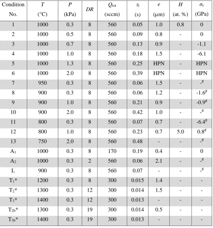
Table Captions
Table 1 : Experimental conditions used for the deposition of the silicon nitride films (QNH3/QSiHCl3 = 5, DR = QH2 + QAr / QSiHCl3 + QNH3, Qtot: total flow rate, r: residence time), e:
thickness (+/- 0.2 m, as measured by SEM), H: hydrogen concentration (as measured by NRA) and σc: residual stress in the film (as measured by Raman spectroscopy). -: not measured, *:
Condition No. T (°C) P (kPa) DR Qtot (sccm) r (s) e (m) H (at. %) σc (GPa) 1 1000 0.3 8 560 0.05 1.0 0.8 0 2 1000 0.5 8 560 0.09 0.8 - 0 3 1000 0.7 8 560 0.13 0.9 - -1.1 4 1000 1.0 8 560 0.18 1.5 - -6.1 5 1000 1.3 8 560 0.25 HPN - HPN 6 1000 2.0 8 560 0.39 HPN - HPN 7 950 0.3 8 560 0.06 1.5 - -♯ 8 900 0.3 8 560 0.06 1.2 - -1.6♯ 9 900 1.0 8 560 0.21 0.9 - -0.9♯ 10 900 2.0 8 560 0.42 1.0 - -♯ 11 800 0.3 8 560 0.07 0.7 - -6.4♯ 12 800 1.0 8 560 0.23 0.7 5.0 0.8♯ 13 750 2.0 8 560 0.48 - - -♯ A1 1000 0.3 8 170 0.19 0.4 - 0 A2 1000 0.3 2 560 0.06 2.1 - -♯ L 900 0.3 8 560 0.07 - - -♯ T1* 1200 0.3 8 300 0.015 1.4 - - T2* 1300 0.3 12 300 0.014 1.5 - - T3* 1400 0.3 12 300 0.013 - - - T2b* 1300 0.3 19 300 0.014 0.5 - - T3b* 1400 0.3 19 300 0.013 - - -
Table 1 : Experimental conditions used for the deposition of the silicon nitride films (QNH3/QSiHCl3 = 5, DR = QH2 + QAr / QSiHCl3 + QNH3, Qtot: total flow rate, r: residence time), e:
thickness (+/- 0.2 m, as measured by SEM), H: hydrogen concentration (as measured by NRA) and σc: residual stress in the film (as measured by Raman spectroscopy). -: not measured, *:
Figure and supplementary material captions
Fig. 1: LPCVD reactor used for the deposition of the silicon nitride films and the FTIR gas phase analyses
Fig. 2: Circular plate loading device for the calibration of the Si Raman peak shift versus pressure difference P
Fig 3: Maximum deflection at the center of a silicon wafer as a function of the pressure difference P, as measured by optical microscopy and calculated by FE analysis
Fig 4: Raman shift of the Si peak as a function of the maximum stress at the center of the wafer (as deduced from the applied pressure difference ΔP)
Fig 5: Arrhenius plot of the deposition rate recorded at different total pressures: P = 0.3, 0.5 and 2.0 kPa (dilution ratio DR = 8 except *: DR = 18)
Fig 6: FTIR spectra recorded at the outlet of the reactor (at ambient temperature) during CVD experiments carried out in condition No. 1 (Table 1) with a slight excess of either (a) SiHCl3)
or (b) NH3
Fig 7: Influence of the partial pressures (a) of SiHCl3 and (b) of NH3 on the deposition rate (P
= 0.3 kPa, T = 1000 °C) and the unreacted proportions of SiHCl3 and NH3 in the gas phase (as
deduced from the IR peak areas measured at the outlet of the reactor)
Fig 8: ATR-IR Si-H and N-H peak areas recorded from the silicon nitride films as a function of T (left, P = 1.0 kPa) and P (right, T = 1000 °C)
Fig 9: X-ray diffraction patterns of (a) an amorphous a-SiNx coating deposited in condition
No.1 (1000°C, Table 1) and (b) a crystalline Si3N4 coating deposited in condition No.T2
Fig 10: Optical micrographs of the surfaces of a-SiNx coatings deposited on Si wafers in
conditions (a) No. 1 (0.3 kPa, 1000 °C), (b) No. 8 (0.3 kPa, 900 °C) and (c) No. 10 (2.0 kPa, 900 °C, see Table 1)
Fig 11: SEM images of the surfaces of coatings deposited in conditions (a) No. 1 (0.3 kPa, 1000 °C), (b) No. 10 (2.0 kPa, 900 °C), (c) No. T2 (0.3 kPa, 1300 °) and (d) No. 5 (1.3 kPa, 1000 °C, see Table 1)
Fig 12: P-T diagram showing the crystalline, cracking and residual stress states in the silicon nitride coatings (see CVD conditions in Table 1). Diamonds (green): crystalline and crack-free, circles (red): amorphous and cracked (♯), squares (blue): amorphous and crack-free, triangles (black): homogeneous phase nucleation (HPN). The open markers size is proportioned to the amount of residual stress in the film (solid markers: stress was not assessed)
SupMat 1: Optical microscopy images at different magnifications of the cross section of a 25
3
1 Gaz inlet (SiHCl
3