HAL Id: hal-00091799
https://hal.archives-ouvertes.fr/hal-00091799
Preprint submitted on 7 Sep 2006HAL is a multi-disciplinary open access archive for the deposit and dissemination of sci-entific research documents, whether they are pub-lished or not. The documents may come from teaching and research institutions in France or abroad, or from public or private research centers.
L’archive ouverte pluridisciplinaire HAL, est destinée au dépôt et à la diffusion de documents scientifiques de niveau recherche, publiés ou non, émanant des établissements d’enseignement et de recherche français ou étrangers, des laboratoires publics ou privés.
NO2 gas sensing studies: Impact of geometrical and
physical characteristics of ohmic contacts on n-InP
epitaxial sensitive layer
Laure Berry, J. Brunet, Christelle Varenne, Lionel Mazet, Alain Pauly,
Katarzyna Wierzbowska
To cite this version:
Laure Berry, J. Brunet, Christelle Varenne, Lionel Mazet, Alain Pauly, et al.. NO2 gas sensing studies: Impact of geometrical and physical characteristics of ohmic contacts on n-InP epitaxial sensitive layer. 2006. �hal-00091799�
NO
2GAS SENSING STUDIES : IMPACT OF GEOMETRICAL AND PHYSICAL
CHARACTERISTICS OF OHMIC CONTACTS ON n-InP EPITAXIAL SENSITIVE
LAYER
L.Berry, J.Brunet, C.Varenne, L.Mazet, A.Pauly, K.Wierzbowska
LASMEA (UMR 6602 CNRS), Université Blaise Pascal Clermont-Ferrand II, 24 avenue des Landais, 63177 Aubière Cedex, France
Email: lberry@univ-bpclermont.fr
Abstract
This paper deals with the influence of technological process steps on electrical and metrological parameters of NO2 gas sensors. The NO2 gas sensors are based on thin n-InP epitaxial layers. The
NO2 gas action makes the resistance of the device, measured in parallel to the surface between ohmic
contacts, increase. It is demonstrated that the methodology of fabrication modifies the geometrical and physical parameters of ohmic contacts and the reproducibility of the devices. The impact on the gas sensors in response to NO2 is also discussed.
Keywords
gas sensor, InP, ohmic contacts, Nitrogen dioxide
1. INTRODUCTION
In view of the pollutants consequences on human health, the detection of the presence and the measurement of toxic gases (such as NO2, O3…) have become essential for environmental protection.
In recent years, the concentration of NOx gases (NO and NO2) in atmosphere has increased with
increase in traffic and the number of buildings. Nitrogen oxides cause lung irritations, decrease the fixation of oxygen molecules on red blood cells, increase the susceptibility to infections, contribute to acid rains and play an important role in the formation of ozone in the lower atmosphere [1].
In air quality monitoring, epitaxial InP based sensors have demonstrated their oxidizing gases (NO2,
O2, O3) detection efficiency [1, 2]. According to previous laboratory experiments [3, 4], the InP based
resistive gas sensor is sensitive to nitrogen dioxide. The resistance of n-InP epitaxial layers, measured parallel to the surface, increases in the presence of NO2. The contacts used with the external circuit
are ohmic, and the action of the gases is restricted to the surface between these contacts [5]. The devices have demonstrated an interesting response and a good lifetime. After several gas tests, the reproducibility of the response for one sensor has been validated. However, with the technological process developed to realize ohmic contacts [1], it was impossible to control the dimensions of the contacts, inducing problems of reproducibility between different samples.
Firstly, the technological process developed to improve the lack of reproducibility between different samples of InP based resistive gas sensors is presented.
Afterwards, the influence on ohmic contact resistance is studied.
In the end, the impact of the technological process on the gas sensors’ response to NO2 is discussed.
Based on two different technological processes, two different gas sensor samples are realised. The sensitivity, the stability and the influence of operating temperature between the two samples are discussed.
2. EXPERIMENTS
2.1. SENSITIVE LAYER
III-V semiconductor sensor is based on a thin n-type InP epitaxial layer, grown by molecular beam epitaxy on a semi-insulating Fe compensated InP substrate. The dimension of the n-InP epitaxial layer is 9mm×18 mm, the thickness of the n–type layer is 200nm and its doping level is ND = 2.1016 cm-3.
In order to measure the resistance of the sensitive layer, ohmic contacts are made.
A particular process was defined to improve the reproducibility of ohmic contacts. Au/Ge/Au ohmic contacts were deposited on InP epitaxial layer by thermal evaporation under vacuum through a stainless steel mask (Fig. 1).
Ohmic contacts with a thickness of 1450Å were made by sequential deposition of Au and Ge under a pressure of 10-7 Torr (Fig. 2). The first two layers were evaporated with a slow rate of 1Å.s-1 to optimize the homogeneity of the layers. Then, the last layer of Au was evaporated with a rate of 2-3 Å.s-1. Finally, the ohmic contacts were submitted to an annealing process under controlled and optimized conditions. The following annealing sequences in H2 (200°C for 3mn, 250°C for 1mn and 300°C for
10s) have been performed for all ohmic contacts. The first annealing homogenized the contacts. The two last annealing formed a thin n+-InP layer at the metal/InP interface, leading to electrically good quality contacts.
2.2. SENSOR DEVICE
To investigate the influence of ohmic contacts on sensor samples reproducibility, stability and sensitivity, two different structures (Fig. 1) were realised.
The sample with 8 ohmic contacts was cleaved in two equal dimension samples with 4 ohmic contacts (the dimension of each sample is 9mm×9mm). In first structure (called S1), Au wires (0.38 µm diameter) were bonded onto Au/Ge/Au ohmic contacts. In the second structure (called S2), the same wires were used with tin balls along side them. Finally the tin balls were attached with silver paste onto Au/Ge/Au ohmic contacts.
Finally, S1 and S2 were joined, with silver paste, to an alumina substrate fitted with a screen-printed Pt resistor on its back side, allowing heating and temperature control (Fig. 3).
2.3. NO
2TEST EXPERIMENTS
For NO2 test experiments, the structures were mounted together in the same stainless steel cylindrical
cell. Measurements were made by recording the resistance variations of the n-type InP. The operating temperature was varied between 80°C and 140°C. During laboratory experiments, the (NO2) test gas
was diluted in dry pure air and its concentration was monitored by mass flow controllers. The total gas flow was kept constant at 50 l/h.
For every gas test experiments, the InP sensors were maintained in darkness because of their light sensitivity, and the sensors’ recorded signal was the resistance of the layer.
Data was recorded every 1 min by a Keithley digital multimeter and then compared with nitrogen dioxide concentrations delivered by a dual chamber chemiluminescent nitrogen oxides monitor (model AC32M, Environnement S.A.).
3. INFLUENCE ON OHMIC CONTACT RESISTANCE
For S1 and S2 structures, we present measurements on contact resistances of Au/Ge/Au ohmic contacts to n-type InP.
The results are discussed to evaluate the dependence of contact resistances on: - the surface and the geometry of the sensitive layer,
- the process used to attach Au wires onto Au/Ge/Au ohmic contacts.
To estimate the impact of the surface and the geometry of the sensitive layer, the resistance between two contacts was measured for a S1 type structure. Each contact was numbered as described in figure 4.
Table1 summarizes the value of the linear electrical resistance measured between contacts 1 and 3 after three successive splittings described in the figure 5. The linear distance between contacts 1 and 3 was measured equal to 3.8mm.
The linear electrical resistance decreases with the reduction of the surface layer. The splitting concentrated on the reduction of the sample perimeter gives information of the repartition of the electric field lines between two contacts. The impact of the surface perimeter on the electrical resistance between two contacts demonstrates the non-linear distribution of the electric field lines. Furthermore, the imperfect linearity of the variation of the linear electrical resistance with the sample surface is probably linked to the non uniform doping level on the whole surface.
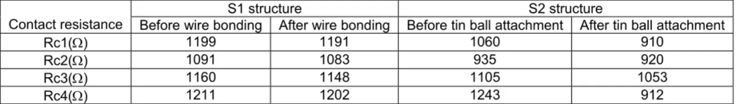
In another experiment, for S1 and S2 structures (Fig. 1), the variation of contact resistance was evaluated before and after wire attachment bonding, and before and after the addition of tin ball (Table2). The contact resistances were defined applying the Van Der Pauw method. The difference in contact resistance between S1 and S2 structures is linked to the geometry of the sensitive layer. For S1 structure, contact resistance is approximately stable before and after wire attachment. For S2 structure, the contact resistance measured after tin balls’ addition is smaller than one measured before. Therefore, the addition of tin ball improves the quality of ohmic contact. However, the reproducibility of S2 structure is not systematically guaranteed.
In NO2 test experiments, how has this difference of the contact resistance influenced on the sensor
behaviour of S1 and S2?
4. INFLUENCE ON NO
2TEST EXPERIMENTS
Amongst all the tested gases (CO, O2, NO2, CH4, Cl2, NH3), it is noted that nitrogen dioxide had the
strongest action on the sensor output. According to our previous laboratory experiments, when an InP layer is exposed to an oxidizing gas such as NO2 (electron acceptor), gaseous molecules get
adsorbed on the InP surface; some of them become negatively ionized (NO2-) by chemisorption. The
formation of these ions induces a repulsive electric field for the majority carriers of n-type InP, creating a depleted zone just below the surface. Consequently, the effective cross-section for the current flow between the contacts is reduced and the resistance increases [3,4,5].
It is well known that increasing the working temperature of a semi-conducting gas sensor improves the speed of adsorption and desorption and, consequently, the response and recovery times [6].
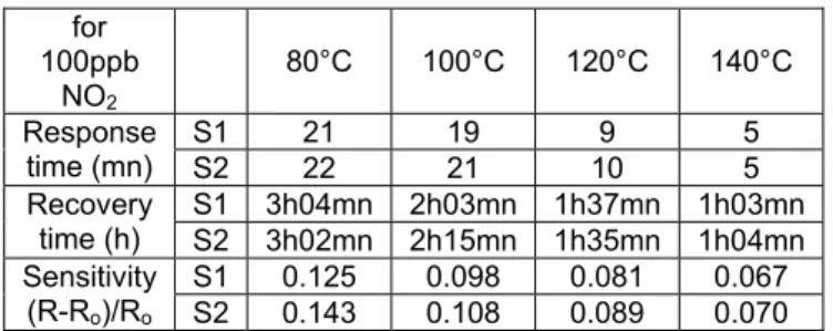
We have studied the effect that temperature has on the response of S1 and S2 structures to different concentrations of NO2: 40ppb, 60ppb, 80ppb and 100 ppb of NO2 diluted in dry pure air.
For S1 and S2 structures, metrological characteristics were estimated:
- the response time : time to reach 90% of the final value under the NO2 gas submission,
- the recovery time : time to fall below 10% of the maximum response after the NO2 gas submission,
- the sensitivity or relative variation of the resistance.
With temperature, the three parameters are nearly same (Table 3). These three parameters decrease with the operating temperature.
Therefore, the difference of the contact resistance between S1 and S2 has no influence on their sensor behaviour. The samples are reproducible because the technological process allows controlling the distance between ohmic contacts and their geometry. This result consolidates the assumption according to which the gas contact interaction can be rejected [3]. However, after several submissions to NO2, it could be interesting to evaluate the stability of ohmic contacts between S1 and S2.
Moreover, the stability of Ro is optimal at 100°C. Below 100°C, the long recovery time leading to an
unstable baseline is problematic for sensor applications. Above 100°C, Ro continuously decreases
(Fig. 6).
After one week of InP submission to NO2 at 140°C, a new test was realised at 100°C. Ro decreased
before and after the experiments at 140°C (Table 4). It could be linked to an irreversible effect.
However, the response to NO2 is nearly the same before and after the experiments at 140°C (Table
4). This result was observed all along the period of tests despite the continuous decrease of Ro. It is
well known that freshly grown InP layers are covered with a very thin oxide layer (≈2nm) as soon as they are exposed to ambient atmosphere, and species such as In2O3 and P2O5 have been identified
[7,8]. This chemically stable layer could induce a permanent depleted zone. In this case, the action of NO2 increases this zone. Resistance varies in the same way as before. However, an influence of the
temperature on the stability of surface oxygen species like In2O3 or P2O5 could explain the effect of the
temperature on the gas sensor response. At 140°C, the continuous decrease of Ro could be linked to
a rearrangement of surface oxygen species not sufficiently stabilised.
The process involved, reversible or irreversible could depend on different time constants. It could be associated with physicochemical parameters of the initial oxide layer which depend on experimental conditions [9].
Recently, XPS spectra (X-ray Photoelectron Spectra) of InP surfaces, before and after NO2
submission, as well as theoretical calculations on surface states (or near surface region at InP surfaces) were developed in the laboratory [10]. The results have demonstrated the development of a complex InP related oxide layer at the surface, which gives rise to the high density of surface states. The surface state and depletion layer influences strongly on the layer sensitivity to ion adsorption. This role of the surface oxide layer on the layer sensitivity could explain the observed Ro instability with
operating temperature. It could be linked to the instability or rearrangement of the surface oxide layer with temperature.
5. CONCLUSION
The technological process developed to optimize the reproducibility of InP sensor samples is based on two principles:
- the control of the distance between ohmic contacts and their geometry,
- the wire bonding technology is optimal for the reproducibility. Even if tin ball attachment improves the quality of ohmic contact, the long term stability of the attachment is not guaranteed in test conditions with gases. An experimental study on the long term stability between the two structures S1 and S2 is needed.
Based on four months experiments, NO2 test experiments reject a gas contact interaction. The study
concerning the influence of the operating temperature on the InP response to NO2 is coherent with
reversible or irreversible process depending on different time constants, which could be associated to the variation of physicochemical parameters of the initial oxide layer with experimental conditions.
References
[1]: L.Talazac, J.Brunet, V.Battut, J.P.Blanc, A.Pauly, J.P.Germain, S.Pellier, C.Soulier, Air quality evaluation by monolithic InP-based resistive sensors, Sensors and Actuators B76, 2001, 258-264 [2]: L.Talazac, F.Barbarin, C.Varenne, L.Mazet, S.Pellier, C.Soulier, Gas sensing properties of pseudo-schottky diodes on p-type indium phosphide substrates : application to O3 and NO2 monitoring
in urban ambient air, Sensors and Actuators B83, 2002, 149-159.
[3]: V.Battut, J.P.Blanc, C.Maleysson, Gas sensitivity of InP epitaxial thin layers, Sensors and Actuators B44, 1997, 503-506.
[4]: L.Talazac, J.P.Blanc, V.Battut, F.Mollot, NO2 sensitivity of thin n-type InP epitaxial layers,
Electron.Technol. 33, 2000, 213-216
[5]: V. Battut, J. P. Blanc, E. Goumet, V. Soulière and Y. Monteil, NO2 sensor based on InP epitaxial
thin layers, Thin solid films, Volume 348, 1999, 266-272.
[6]: M.Dugay, C.Maleysson, Thin layers of poly(fluoroaluminium-phtalocyanine), Synthetic Metals, 21, 1987, 255-260.
[7]: S.Selci, A.Cricenti, A.C.Felici L.Ferrari, C.Goletti, G.Chiarotti, Oxygen chemisorption on cleaved InP (110) surfaces studied with surface differential reflectivity, Phys.rev., B43 - 8, 1991, 6757-6759 [8]: D.X.Dai, F.R.Zhu, Auger-electron spectroscopy, electron-energy-loss spectroscopy, and x-ray photoemission spectroscopy studies of oxygen adsorption on the InP (111)-(1×1) surface, Phys.Rev., B43 – 6, 1991, 4803-4808.
[9]: A.Gurlo, N.Bârsan, M.Ivanovskaya, U.Weimar, W.Göpel, NO2 detection by a resistive device
based on n-InP epitaxial layers, Sensors and Actuators B: Chemical, Volume 47, Issues 1-3, 1998, 92-99
[10]: K.Wierzbowska, B.Adamowicz, L.Mazet, J.Brunet, A.Pauly, L.Bideux, C.Varenne, L.Berry, JP.Germain, High-sensitivity NO2 sensor based on n-type InP epitaxial layers, Optica Applicata,
hole ∅=1mm Stainless steel mask Au/Ge/Au ohmic contact n-InP epitaxial layer S1 structure S2 structure Au wires bonded onto Au/Ge/Au contact Au wires along with tin ball, attached to Au/Ge/Au contact Semi-insulating substrate 20mm 10mm 9mm 18mm 9mm 9mm
n-InP epitaxial layer Au (1000Å) Ge (350Å) Au (100Å)
Heating and temperature control Ag paste Alumina heating substrate S1 or S2
1
2
3
4
9.8mm 9.1mm
9.8mm 9.1mm
1
3
5 mm 9.1mm splitting 11
3
5 mm 7mm splitting 21
3
3.5 mm 7mm 5.5 mm 2.8 mm 0.7 mm splitting 34.0 4.2 4.4 4.6 4.8 5.0 5.2 5.4 5.6 temps(heure) 10 21 31 41 52 62 72 83 93 time (hours) R(k o hm ) 40 ppb 60 ppb 80 ppb 100 ppb 80 ppb 60 ppb 40 ppb operating temperature : 100°C operating temperature : 140°C S1 S1 S2 S2 0
step Linear electrical
resistance (kΩ) sensitive layer surface (mm2)
Splitting 1 R13 = 8.9 45.5
Splitting 2 R13 = 10.8 35.0
Splitting 3 R13 = 11.5 23.5
S1 structure S2 structure
Contact resistance Before wire bonding After wire bonding Before tin ball attachment After tin ball attachment
Rc1(Ω) 1199 1191 1060 910
Rc2(Ω) 1091 1083 935 920
Rc3(Ω) 1160 1148 1105 1053
Rc4(Ω) 1211 1202 1243 912
for 100ppb NO2 80°C 100°C 120°C 140°C S1 21 19 9 5 Response time (mn) S2 22 21 10 5 S1 3h04mn 2h03mn 1h37mn 1h03mn Recovery time (h) S2 3h02mn 2h15mn 1h35mn 1h04mn S1 0.125 0.098 0.081 0.067 Sensitivity (R-Ro)/Ro S2 0.143 0.108 0.089 0.070
for 100ppb NO2 100°C 140°C 100°C S1 19 5 18 Response time (mn) S2 21 5 19 S1 2h03mn 1h03mn 2h07mn Recovery time (h) S2 2h15mn 1h04mn 2h17mn S1 0.098 0.067 0.094 Sensitivity (R-Ro)/Ro S2 0.108 0.070 0.099 S1 5.0 4.0 4.4 Ro