Design of Energy-Saving PZT Drive Amplifiers
for Mobile and Wearable Physical Assists
The MIT Faculty has made this article openly available.
Please share
how this access benefits you. Your story matters.
Citation
Barragán, Patrick R., et al. “Design of Energy-Saving PZT Drive
Amplifiers for Mobile and Wearable Physical Assists.” ASME
2011 Dynamic Systems and Control Conference and Bath/ASME
Symposium on Fluid Power and Motion Control, Volume 2, 31
October - November 2, 2011, Arlington, Virigina, ASME, 2011, pp.
783–90. © 2011 by ASME
As Published
http://dx.doi.org/10.1115/DSCC2011-5977
Publisher
ASME International
Version
Final published version
Citable link
http://hdl.handle.net/1721.1/118911
Terms of Use
Article is made available in accordance with the publisher's
policy and may be subject to US copyright law. Please refer to the
publisher's site for terms of use.
DESIGN OF ENERGY-SAVING PZT DRIVE AMPLIFIERS FOR MOBILE AND WEARABLE
PHYSICAL ASSISTS
Patrick R. Barragán Shinichiro Tsukahara H. Harry Asada Mechanical Engineering Massachusetts Institute of TechnologyCambridge, Ma 02139 {barragan, tsukahar, asada}@mit.edu
ABSTRACT
An energy-efficient circuit for driving PZT actuators using a charge recovery technique is explored in this paper. Mobile and wearable devices for physical assists requiring extended battery life and/or minimal battery weight will benefit from this technology. PZT is a capacitive transducer and can produce constant force for extended periods with little power consumption. Furthermore, energy can be saved by moving charge from one PZT stack to another instead of draining to ground. This paper describes an efficient charge-recovery circuit that can capture 40~65% of the energy in one PZT unit by transferring it to another PZT unit. The battery then must only supply the remaining charge thereby increasing battery life. First, the basic principle of the charge-recovery technique is described. The idealized circuit architecture and possible implementation are presented. Then, the electrical circuit behavior is analyzed. PZT hysteresis is discussed, and results are presented.
INTRODUCTION
Energy saving is a critical issue for battery powered mobile and wearable devices. In particular, physical aids and rehabilitation equipment, including prosthetic devices, rehabilitation training equipment, and exoskeletons, need energy-efficient, compact actuators that can bear a large torque load for long durations. Piezoelectric actuators, such as Lead Zirconate Titanate (PZT) stacks, are well suited for maintaining constant loads. As a capacitive transducer, PZT can produce a force while charge is stored in the material. Because of the slow leak of this charge, PZT actuators consume little energy in maintaining an output force or torque unlike electromagnetic actuators which consume significant energy in this context. This feature may be
useful for a type of mobile and wearable assists where a large force/torque load must be borne for long periods. Examples include holding a constant posture, moving a load slowly or intermittently, and locking or clamping a joint. Prosthetic arms and legs, physical aids, and elderly support devices are often operated under these static conditions or in quasi-static modes. Energy saving will be substantial if only limited energy is consumed during these periods.
Despite the excellent static load bearing capacity, only a fraction of electric energy stored in a PZT stack is converted to mechanical energy. The coupling factor, the ratio of mechanical energy in the volume to electrical energy supplied, is much smaller than 1, and thus much of the electrical energy driven to the actuator is not converted to mechanical energy [1,2]. As the actuator is capacitive in nature, some fraction of this unused, stored electrical energy can be recovered [3]. [1] presented a possible recovery circuit to drive this unused energy to another piezoelectric element using an inductor to achieve a theoretically 100% energy efficient transfer. This method is very useful for moving energy between two piezoelectric elements which are actuated 180º out of phase. The circuit can provide large energy savings which become especially important at high actuation frequencies.
The charge-recovery technique can be understood better and improved by analyzing parasitic effects of the major components of the circuitry as well as the nonlinearity of the PZT stacks. The aim of this paper is to expand the use of this circuit to PZT stack actuators used in large strain applications. More detail on implementation will be explored. Important for circuit optimization, inherent loss mechanisms including hysteresis will
Proceedings of the ASME 2011 Dynamic Systems and Control Conference DSCC2011 October 31 - November 2, 2011, Arlington, VA, USA
be examined and supported with measured data. Finally, future work on this topic will be discussed.
CHARGE RECOVERY PRINCIPLE FOR PZT ARRAY ACTUATORS
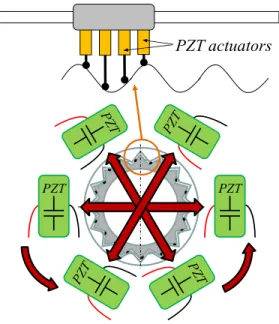
Traditionally, PZT actuators are used primarily for fine positioning and small load applications. These include precision positioning stages, ink jet printers, and fuel injection valves. For large motion applications, they are used with a friction-drive mechanism, where an array of PZT elements is pressed against a rotor plate with a preload, as seen in ultra-sonic actuators. Due to their extremely small strain, however, the preload must be set at a proper level, which limits the application to only small and constant loads. This limitation can be removed with effective strain amplification mechanisms which can create displacement amplification gains of over 100 times the original PZT stroke [4,5]. This allows a PZT unit to thrust a load surface directly in the normal direction rather than tangentially through surface friction. Figure 1 illustrates a PZT array actuator rotating a spur-gear like disk where individual PZT actuators press on different sections of the gear to create the rotational motion. The details are described in a prior paper [6] as well as in a companion paper [7].
One salient feature of this type of arrayed PZT actuators is that multiple pairs of PZT units are coordinated spatially as well as temporarily to produce a continuous motion. Each PZT unit repeats a charging and discharging cycle with a phase angle shifted from its adjacent unit. As shown in Fig. 1, the individual PZT units can be grouped into multiple pairs having charging-discharging cycles that are 180º out of phase. Pairing these PZT units allows us to apply the aforementioned charge-recovery technique effectively. Each PZT unit may have multiple PZT stacks. This work will assume that pairs of these units are chosen for use in the circuit design presented.
PZT actuators
PZT PZT
FIGURE 1. ARRAYED PZT ACTUATOR ROTATING A GEAR. PAIRS HAVE 180º PHASE DIFFERENCE
The circuit requires the functionality to charge and discharge each PZT unit separately and also to allow energy transfer from one unit to the other in either direction separately. The circuit discussed below is only one solution to achieve these functionalities and was chosen because of its simplicity and theoretical full charge transfer.
CIRCUIT IMPLEMENTATION Idealized Circuit Architecture
The circuit in Fig. 2 was originally presented in [1] as an architecture to drive energy from a capacitance C1 to another C2.
Transfer schemes have one element (in this case C1) charged to a
voltage Vo and then connected in some manner to the second
element (in this case C2). Simply connecting these two
capacitances together directly will cause their voltages to equilibrate. The case of interest shown later is in which C1 = C2 = C. Regardless of the level of resistance in the connection, 50% of
the energy will be lost. The energy goes as the voltage squared. With both voltages equal at half of the initial voltage Vo on C1,
only 25% on the initial energy on C1 now exists on C2. By adding
an inductor in line with the transfer, a LC tank is created. In the no-resistance case, the oscillations that arise can transfer 100% energy between the capacitances. Then, by adding a diode to the transfer path, the oscillation is stopped after one half-period. Again, in the no-resistance case, at this point, C2 will be driven to Vo, and C1 will have no voltage. The two diodes and two switches S12 and S21 are required to transfer charge in either direction
depending on which capacitance is originally charged.
FIGURE 2. IDEALIZED CIRCUIT
With resistance, the circuit operates as a series RLC exhibiting a damped oscillation. After one half-period, C2 will rise
to its highest voltage during this oscillation making the diode method still applicable. However, C1 does not reach zero voltage.
The additional switches arranged in a half-bridge configuration on each side allow the high and low voltage rails to completely charge or discharge respectively the appropriate capacitance after the incomplete transfer.
A Possible Circuit Implementation
[1] gives part numbers used for certain components of the circuit implemented. To expand on the available information for
this architecture, a possible circuit implementation is presented here with some explanation for the design choices. This implementation hopes to serve as a guide or suggestion but is only one of many possible implementations each with their own advantages and disadvantages.
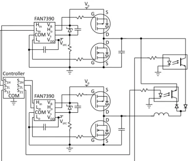
Figure 3 shows the full circuit implementation developed. Fairchild FAN7390 gate drivers were used to drive the high and low side MOSFETs to implement the two half bridges (S1H, S1L
and S2H, S2L). In standard high side drive circuits, N-FETs can be
used for both the high and low side switch. However, the chip architecture for many high-side drivers causes the node between the switches to be tied through the chip to the chip supply voltage. This node can never be completely disconnected and float. In this application, the capacitances must be able to float when not connected to either rail. To avoid this problem, P-FETs were used instead. The zener diode and capacitor setup seen for each half-bridge uses the high voltage rail Vo to generate the necessary
bootstrap voltage used by the high-side drive circuitry. This approach is suggested by [8].
Because the transfer switches S12 and S21 must float with the
capacitances, opto-couplers were utilized. Although opto-couplers generally require more power than MOSFETs, energy usage in the opto-couplers is minimal because of the short duration of on-time needed for transfers (~5 [ms] for this implementation).
Controller S1H S1L S12 S2H S2L S21 COM FAN7390 Hin Lin COM Lo VB Ho Vs VDD G S D G D S Vsrc Vo G S D G D S Vsrc Vo FAN7390 Hin Lin COM Lo VB Ho Vs VDD
FIGURE 3. CIRCUIT IMPLEMENTATION
CIRCUIT DESIGN OPTIMIZATION
The above circuit experiences many loss mechanisms in its different subsystems. This work will focus on the losses existing in the transfer of energy between capacitors. To optimize the entire circuit, careful choice of component values and chips is required. Other implementations could be created which could further
minimize required battery energy. However, this paper’s goal is to compare the use of this transfer mechanism to a simple charge-discharge actuation scheme with no attempt at recovery and discuss certain details of the losses and optimization. In both schemes, half-bridges would likely be used and thus are not the center of focus. Also, the switch implementation choices for the transfer switches may be improved using different switches or a different architecture. This work will focus on the electrical characteristics of the transfer once a path from one capacitance through the diode and inductor to the other capacitance is established.
Ideal Capacitor Case
A simple model of the electrical behavior of a PZT stack actuator is an ideal capacitor. This model proves inaccurate due to pronounced hysteresis existing in the material. However, the simple model still provides a good base for analysis of this design. To expand slightly for the ideal case with no resistance, some series resistance for the capacitances and inductor is assumed. As described in [1], if these components operate in their linear range, these resistances can be lumped into one Req. Although this
assumption may fail in the case of the nonlinearities in PZT, linear analysis provides a good base to explore the circuit’s behavior.
As to analyze the entire oscillation, the diode will be left out of the following. The diode will contribute some small resistance and a small forward voltage (compared to the PZT operating voltage) to the final circuit which must be considered in a final design. Without the diode, the circuit considered for the rest of this analysis is shown in Fig. 4.
S
2C
1C
L
eqR
FIGURE 4. SIMPLIFIED RLC CIRCUIT
At time t = 0, C1 is charged to voltage Vo and the switch
closes. The switch remains closed and the RLC oscillations occur. As an example, Fig. 5 shows the damped oscillation for Vo = 100
[V], C1 = C2 = C = 13.6 [µF], L = 500 [µH], and R = 2 [Ω].
As shown, the voltages oscillate around a steady state value at half of the original Vo. With damping, the oscillations decay until
both capacitances have equal voltages at this steady state value
VSS. The height of the first peak of the voltage on C2 is denoted VH
which occurs after one half-cycle of oscillation. With the diode in place, the oscillation ideally will stop at this value as at this point, the current through the diode would become negative. Therefore,
0 0.5 1 1.5 2 2.5 3 x 10⁻³ 0 10 20 30 40 50 60 70 80 90 100 Time [s] V o lta g e [V ] VC 1 VC 2 VSS VH FIGURE 5. RLC OSCILLATION
The transfer efficiency is defined in Eq. (1) as the ratio of final energy on C2 after transfer over the initial energy on C1
before the transfer.
2 2 2 1 final H initial o
E
C V
E
C V
(1)In general, the transfer can also occur in the opposite direction depending on initial conditions which would simply flip the capacitances in the above efficiency definition. For simplicity, this discussion will be restricted to transfers as stated above.
V2(t), the voltage across C2, can be derived from standard
circuit theory as 2 2 2 2 1 1 1 ( ) t( sin( ) cos( )) 1 o V t V e t t C L (1)
where α and β are given by
2
,
1
n n
(3)respectively. The parameters in Eq. (3) are in terms of the natural frequency of the system ωn and the damping ratio of the
oscillation ζ given by
1
1
,
2
eq n eq eqC
R
L
LC
(4)respectively, where Req is the total equivalent series resistance and
eq
C
is the equivalent capacitance given by1 2 1 2 eq
C C
C
C
C
(5)Given in Eq. (6), the first peak voltage VH occurs at time t = π/β. 2 1 1 1 2
1
H oC
V
V e
C
C
(6)Equation (6) gives insight to the important factors dictating the high transfer voltage VH. Assume C1 is set at some value.
Decreasing C2 increases the capacitance ratio term and also
decreases Ceq and therefore ζ. Overall, decreasing C2 increases VH.
However, as shown in Eq. (1), the transfer efficiency relies on increasing Efinal on C2 after the transfer. Efinal is given by
2 2
1
2
final HE
C V
(7)Substituting Eq. (6) into Eq. (7) yields
2 2 2 1 2 2 1 2 1 2
1
1
2 (
)
final oC C
E
V
e
C
C
(8)Equation (8) gives the optimal choice of C2 for a set of given
circuit parameters. As seen in Fig. 6 for C1 = 13.6 [µF], the
optimal C2 = 11.6 [µF] is not equal to C1 although in this example,
the values are close. Although VH continues to increase for small C2, the final energy has an optimal value. More importantly, in
many applications, the transfer must be bidirectional. In this context, optimality of one transfer in each direction from full Vo
dictates that in fact C1 should equal C2. The remaining analysis
will only consider this equal capacitance case of C1 = C2 = C = 2Ceq.
Rewriting Eq. (1) for the equal capacitance case gives
2 final H initial o
E
V
E
V
(9)Thus, optimizing VH for a given Vo becomes equivalent to
optimizing the transfer energy efficiency. Similarly rewriting Eq. (6) for this special case yields
2 1
1
1
2
H oV
V e
(10)which requires minimizing ζ to maximize VH for a given Vo.
Equation (4) shows that decreasing Req or Ceq or increasing L will
decrease ζ. If C is dictated by the actuator, Ceq and the resistive
contribution of the actuator to Req are determined. Then in the
simplest case, optimization of the transfer requires choosing a sufficiently large L with sufficiently low parasitic resistance RL,
the inductors resistance contribution, to meet the design requirement. 1 2 3 4 5 6 7 8 9 10 x 10-5 0 0.1 0.2 0.3 0.4 0.5 0.6 0.7 0.8 0.9 1 C2 [F] N or m al ize d fir st p ea k vo lta ge a nd tr an sf er e ffi ci en cy VH/Vo max VH/Vo max
FIGURE 6. NORMALIZED FIRST PEAK VOLTAGE AND TRANSFER EFFICIENCY VS. C2
This design process is far oversimplified for any practical application. If the efficiency of the transfer is denoted Metric 1, two other metrics, at least, may play an important role in the design of a final system. As stated above, Metric 1 would drive the design to have an extremely large L with a small RL which would
often imply an inductor with many turns (for large L) of large diameter wire (for small RL). However, the size of such an
inductor can become prohibitive. Therefore, Metric 2 will be the size and weight of the circuit. A third important metric may also be considered. Equation (4) shows that for a given Ceq, the natural
frequency ωn of the oscillation decreases for increasing L. ωn
dictates the rise of the voltage on the receiving capacitance which in the case of PZT actuators causes the actuation. If the desired application requires an actuator bandwidth ωb, ωn must be much
larger than ωb to accommodate this requirement. Thus, Metric 3
becomes the achievable actuator bandwidth in terms of electrical actuation speed.
Only considering Metric 1 does not sufficiently constrain the optimization of the parameters L and RL. However, the practical
requirements presented by Metric 2 and Metric 3 better constrain the optimal choices of the inductor. The relative importance of the
metrics is of course based on the specific application, and many applications may also introduce additional metrics which must be accounted for in the electrical design.
PZT Stack Actuator
Although the simple analysis presented above of the electrical behavior of the transfer circuitry provides good insight into the true behavior, important loss mechanisms, especially hysteresis, are ignored. Many aspects of the electrical and mechanical hysteresis of PZT have been extensively studied, and models have been developed to describe this behavior with varying levels of complexity [1,9]. For example, [1] employs a model of the PZT as a set of RLC branches representing mechanical modes in parallel with a single RC branch representing the dielectric and successfully uses the model to predict the energy transfer behavior for Vo = 40 [V].
This work will focus on experimental results for PZT stack actuators driven to various voltage levels including voltages near the maximum allowable. A charge versus voltage plot clearly shows the PZT hysteresis. Figure 7 shows these curves for NEC-Tokin AE1010D44H40F PZT stack actuator driven with a sinusoidal voltage from zero to different peak amplitudes. This particular stack has a maximum allowable voltage of 150 [V] and a nominal capacitance of 13.6 [µF]. The upper left portion of each curve corresponds to the charging phase in a cycle while the lower right portion corresponds to the discharging phase.
0 0.5 1 1.5 2 2.5 x 10⁻³ -20 0 20 40 60 80 100 120 140 Charge [C] V o lta g e [V ] Vpeak = 40 [V] Vpeak = 100 [V] V peak = 140 [V]
FIGURE 7. CHARGE VS. VOLTAGE HYSTERESIS LOOPS As the driving voltage for the stacks increases, the shape of the charge-voltage loops changes. At low peak voltages, the curves are approximately symmetric about a line drawn from tip to tip. However, as the voltage increases, the loop begins to bend and is no longer symmetric about a line connecting the two tips.
To simplify experiments, the circuit in Fig. 4 was built to measure the relevant energy transfer signals. The switch S is implemented by an opto-coupler, and no explicit component Req is
added. Rather, Req exists because of parasitic effects in the other
circuit components. Small sense resistors are placed below each capacitance to measure the current. Measuring the current could also be done by numerically integrating the voltage across the inductor [1]. To charge C1 to the initial condition Vo, an additional
switch connects C1 to a voltage source. During each experiment, C1 is charged to Vo with the voltage source, the source then
disconnects from the circuit, and then the switch S closes to allow oscillations to occur. The voltages across the capacitances and sense resistors are measured and used for analysis.
Figure 8 shows an example of capacitance voltages measured during an experiment with Vo = 140 [V] utilizing the above
mentioned PZT stacks as C1 and C2.
0 0.5 1 1.5 2 2.5 x 10⁻³ 0 50 100 150 Time [s] V o lta g e [V ] VC 1 VC 2
FIGURE 8. PZT STACK VOLTAGES FOR VO = 140 [V]
For comparison, experiments were also run with electrolytic capacitors of the same capacitance as the PZT’s nominal value. Figure 9 shows the voltage traces for C2 as a comparison between
the transfer dynamics with capacitors or real PZT stacks.
0 0.2 0.4 0.6 0.8 1 1.2 1.4 1.6 1.8 2 x 10⁻³ 0 20 40 60 80 100 120 Time [s] V o lta g e [V ] PZTs Capacitors
FIGURE 9. RECEIVING CAPACITOR COMPARED TO PZT
One clear difference between the traces is that even at high voltages, the steady state value of the oscillation with capacitors is approximately half of Vo as expected. Conversely, the steady state
value of the oscillation with PZT stacks is significantly lower. Table 1 summarizes the results for the experimental versus predicted values (using Eq. (10)) of VH and VSS. All values are in
the units [V]. Experiments were run with three initial voltages Vo
of 40 [V], 100 [V], and 140 [V] using both the electrolytic capacitors as a baseline and the PZT stacks. The stacks were unloaded in the PZT experiments. Equation (10) was used to predict values for the ideal capacitor case. To explore how accurate the model could perform, in the calculation, L and C were left as their nominal or measured value and Req was left as a free
parameter. Req = 2.7 [Ω] produces the minimum mean squared
error between the prediction and the capacitor case. Various instruments measure the total series resistance of the transfer path differently, but all measurements are on the same order as Req
above. For the worst case of the three, Vo = 140 [V], the energy
transfer efficiency η as defined in Eq. (9) is ~42% for the PZT stack case. For the best case of the three, Vo = 40 [V], η ≈ 59%.
TABLE 1. COMPARISON OF PREDICTED, CAPACITOR, AND PZT EXPERIMENTS. ALL VALUES IN UNITS [V]
Prediction Capacitor PZT Stack
Vo VH VSS VH VSS VH VSS
40 32.6 20 32.2 19.9 30.8 19.1 100 81.6 50 82.2 50.7 69.5 40.9 140 114.3 70 114.48 70.4 91.1 51.2 For the value of Req chosen, the prediction of VH and VSS is
very close to the measured values with a mean squared error (MSE) in VH of 0.22 for the capacitor case. However, the
prediction shows an increasing error for higher voltages when compared to the PZT stack experimental results. Changing to Req
= 6.1 [Ω] produces the minimum MSE of 7.33 when comparing the prediction to the PZT stack results. Yet, as shown by the much higher MSE, the predicted voltages VH for each Vo (VH = 26.8
[V], 66.9 [V], and 93.7 [V] for Vo = 40 [V], 100 [V], and 140 [V]
respectively) no longer closely correspond to the measured values (up to ~13% error compared to ~1% error predicting VH with the
initial Req for capacitor experiments). The ideal capacitor case
does not appear to properly predict VH values for PZT stack
transfer oscillations even with Req as a free parameter.
Furthermore, the ideal capacitor model does not predict the variation in VSS as seen the PZT stack data. For any choices of
parameters, this model always predicts a steady state voltage at half of the initial voltage. The capacitor results closely reflect this prediction. However, for large Vo, the PZT results show a droop in
parameter model in [1] correctly predicts the oscillations seen for relatively low Vo (40 [V]), the hysteresis model given does not
appear to predict any difference in VSS from half of Vo for any
voltage level.
Although this and other models are inadequate to predict this
VSS droop, the droop can be predicted experimentally after
characterizing the desired PZT stack actuator. Returning to the experiments performed to generate Fig. 7, comparing the capacitance versus voltage from the charge and discharge phases of a cycle gives insight into the steady state voltage droop. In Fig. 7, the local slope of the curves at any point is the inverse of the capacitance. The capacitance at a given voltage during the charge and discharge portions of the curve can be calculated using the constitutive relationship of a capacitor.
As an example, the branch modeled used in [1] (including the paper’s choices of model parameters) was simulated. Figure 10 shows the simulated voltage versus capacitance curve for this 5-branch equivalent circuit representing the PZT dielectric and first four mechanical modes. The simulation was performed with the moderately high voltage Vpeak = 100 [V] for the sinusoidal
excitation. The leg of the curve from bottom left to top right corresponds to the charging phase of the cycle while the leg from the bottom right to top left corresponds to the discharging phase. This approximate shape for this type of curve can be qualitatively verified by visually inspecting the change in slope in Fig. 7 for the
Vpeak = 40 [V] curve. 0 10 20 30 40 50 60 70 80 90 100 2.63 2.635 2.64 2.645 2.65 2.655 2.66 2.665 2.67x 10 -8 Voltage [V] C a p a ci ta n ce [F ]
FIGURE 10. SIMULATED VOLTAGE VS. CAPACITANCE FOR BRANCH MODEL
As shown, the two legs intersect at a voltage of one half of the peak voltage used. Clearly, this point corresponds to equal capacitances for the charging and discharge phases of the cycle. Stated another way, this point corresponds to the voltage where the slope of the charge-voltage curve for the charge and discharge phase are equal. The symmetry of this curve and thus its
intersection at Vpeak/2 corresponds to the case where the hysteresis
in the charge-voltage curve is symmetric about a line drawn between the two tips of the curves. This symmetry is the case in the Vpeak = 40 [V] experiment in Fig. 7.
In the case of ideal capacitors or capacitors with equivalent series resistance, the symmetry remains for high peak voltages. However, clearly shown for the higher voltages in Fig. 7, this symmetry is lost in the PZT stack case. Generating voltage versus capacitance curves corresponding to the three loops given in Fig. 7 gives insight into the VSS droop phenomenon observed earlier.
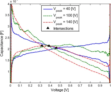
Figure 11 plots the corresponding C vs. V curves (with normalized voltages for comparison). As shown, the intersection point of the different curves occurs at lower and lower percentages of the peak voltage. This result can also be seen in Fig. 7 by finding the voltage in which the slope on each section of the curve is equal. Due to the lack of symmetry of these charge-voltage curves for high Vpeak, this equal-slope point does not occur at Vpeak/2.
0 0.1 0.2 0.3 0.4 0.5 0.6 0.7 0.8 0.9 1 1 1.5 2 2.5 3 3.5 4x 10 -5 Voltage [V] C a p a ci ta n ce [F ] Vpeak = 40 [V] Vpeak = 100 [V] Vpeak = 140 [V] Intersections
FIGURE 11. VOLTAGE NORMALIZED BY VO VS.
CAPACITANCE CURVES FOR PZT STACKS
The absolute intersection voltages occur at 18.1 [V], 38.7 [V], and 44.2 [V] for Vo = 40 [V], 100 [V], and 140 [V]
respectively. These intersection values correspond closely to the steady state voltage values VSS listed in Tab. 1 although the
intersection value for Vo = 140 [V] is slightly lower than VSS
measured in the oscillation experiment.
From this data, the non-symmetric PZT hysteresis at higher voltages appears to cause the drooping of the steady state voltage. This drooping causes the corresponding droop in the VH values for
the PZT experiments compared to the capacitor experiments. Thus, simply by characterizing the PZT actuator of choice up to its maximum allowable voltage, the steady state droop can be estimated. Although a specific method is not mentioned here, this droop must then be related to the droop in VH. Then, the efficiency
of the energy transfer can be estimated. For an accurate measure of the efficiency, the injected charge into the receiving PZT stack must be measured as the capacitance is not constant disallowing the simple use of the standard capacitor energy equations. However, the above characterization gives insight into the expected circuit deviations from the ideal case. With proper measurements, an estimate may be generated for the energy transfer efficiency η.
Furthermore a model which can correctly predict the non-symmetric hysteresis shape of PZT at higher voltages could be used to determine these intersection points in simulation. For example, the model presented in [9] properly demonstrates non-symmetric hysteresis although the model was not tested here. FUTURE WORK
The explanation of the exact relationship between the crossing point in the PZT stacks voltage-capacitance curve and VSS
is incomplete. In addition, in the asymmetric hysteresis case, the exact relationship between VSS and VH, crucial for energy
efficiency prediction, is incomplete. Many models exist to approximately or very accurately describe the PZT behavior. The choice of the most appropriate and practical model that balances simplicity with accuracy or the creation of a new model to form these relationships is the aim of future work. Additionally, the effects on transfer efficiency of loading the PZT actuators must be explored.
CONCLUSION
The circuit topology discussed can efficiently transfer charge from one capacitance to another. In the case of multiple PZT stacks actuated at different times, this topology can increase the electrical efficiency of the system by reusing charge from once PZT stack for partially actuating another. A possible implementation of the circuit was given as an example or guide for future exploration of the circuit or its optimization. The governing equations of the transfer oscillations are shown which can readily predict the transfer efficiency in the case of constant capacitance with some parasitic series resistance. The role of the circuit parameters in this transfer efficiency is clarified from previous work, and three metrics are presented which can fully constrain the parameter value choices for a given application.
Then, the losses due to non-constant capacitance and PZT charge-voltage hysteresis are explored. Previous models have accurately predicted the circuit performance for low voltages. Considerations for high voltage such as droop in the steady-state oscillation voltage and transfer efficiency are discussed. Characterization of the PZT stack of choice can predict
approximate values for the steady-state voltage. The importance of connecting these predictions to predicting the transfer efficiency is clear and is a subject of future work.
Because of the small electromechanical coupling
coefficient of PZT, each actuation cycle requires much unused
electrical energy. The circuit topology presented can provide a means of reusing this energy in certain actuating schemes with transfer efficiencies of 40-65% before circuit optimization. REFERENCES
[1] Campolo, D., Sitti, M., and Fearing, R. S., 2003. “Efficient Charge Recovery Method for Driving Piezoelectric Actuators with Quasi-Square Waves”. IEEE Transactions on
Ultrasonics, Ferroelectrics, and Frequency Control, 50(3),
pp. 237-244.
[2] Wang, Q. M., Du, X. H., Xu, B., Cross, L. E., 1999. “Electromechanical Coupling and Output Efficiency of Piezoelectric Bending Actuators”. IEEE Transactions on
Ultrasonics, Ferroelectrics, and Frequency Control, 45(3),
pp. 638-646.
[3] Main, J. A., Newton, D. V., Massengill, L., and Garcia, E., 1996. “Efficient power amplifiers for piezoelectric applications”. Smart Materials and Structures, 5(6), pp. 766-775.
[4] Secord, T. W., and Asada, H. H., 2010. “A Variable Stiffness PZT Actuator Having Tunable Resonant Frequencies”. IEEE
Transactions on Robotics, 26(6), pp. 993-1005.
[5] Neal, D., and Asada, H. H., 2009. “Nonlinear, large-strain PZT actuators using controlled structural buckling”. IEEE
International Conference on Robotics and Automation, pp.
170-175.
[6] Neal, D., and Asada, H. H., 2010. “Phased-Array Piezoelectric Actuators Using a Buckling Mechanism Having Large Displacement Amplification and Nonlinear Stiffness”.
IEEE International Conference on Robotics and Automation,
pp. 1661-1667.
[7] Torres, J., Neal, D., and Asada, H. H., 2011. “A PZT Array Actuator Using Buckling Strain Amplification and Preload Mechanisms”. Dynamic Systems and Control Conference, in review.
[8] Clemente, S., and Dubhashi, A., 2007. “HV Floating MOS-Gate Driver ICs”. AN-978, http://www.irf.com/technical-info/appnotes/an-978.pdf.
[9] Goldfarb, M., and Celanovic, N., 1997. “Modeling Piezoelectric Stack Actuators for Control of Micromanipulation”. IEEE Control Systems Magazine, 17, pp. 69-79.
![Figure 8 shows an example of capacitance voltages measured during an experiment with V o = 140 [V] utilizing the above mentioned PZT stacks as C 1 and C 2](https://thumb-eu.123doks.com/thumbv2/123doknet/14686840.560437/7.918.69.424.354.636/figure-example-capacitance-voltages-measured-experiment-utilizing-mentioned.webp)