Design and Simulation of a PCI Express Gen 3.0
Communication Channel
By MASSACHUSETTS INSTITUTE OF TECHNOLOGY Dilini WarnakulasuriyarachchiAUG 2
4 2010
S.B. Electrical Science & Engineering
LIBRARIES
Massachusetts Institute of Technology, 2009 ARCHIVESSUBMITTED TO THE DEPARTMENT OF ELECTRICAL ENGINEERING AND COMPUTER SCIENCE IN PARTIAL FULFILMENT OF THE REQUIREMENTS FOR THE DEGREE OF
MASTER OF ENGINEERING IN ELECTRICAL ENGINEERING & COMPUTER SCIENCE AT THE MASSACHUSETTS INSTITUTE OF TECHNOLOGY
MAY 2010
UNuvne Z010 I
0 2010 Massachusetts Institute of Technology. All rights reserved.
Signature of Authoi
Department of Electrical Engineering and Computer Science
May 7, 2010
Certified by:
Scott Westbrook Senior Member of the Technical Staff, NetApp VI-A Company Thesis Supervisor
Certified by: _ _ _ _ _ _ _ _ _ _ _ __ _ _ _ _ _ _ _ _ _ _ _
Vladimir Stojanovic Associate Professor, Department of Electrical Engineering and Computer Studies MIT Thesis Supervisor
Accepted by:
J1
Dr. Christopher J. Terman Chairman, Department Committee on Graduate Theses
Dr. Christopher J. Terman
Department of Electrical Engineering and Computer Science Room 3 8-476, M.I.T.
Cambridge, MA 02139
Subject: Master of Engineering Thesis of Dilini Warnakulasuriyarachchi
Dear Dr. Terman:
I have reviewed the attached thesis of Dilini Warnakulasuriyarachchi on behalf of NetApp. The thesis is within the scope of the thesis proposal as previously approved and does not contain any material that is objectionable to NetApp. It is also approved for its technical content.
It is understood that the actual thesis document will be the permanent property of M.I.T. and will be placed in the M.I.T. Library within one month after the date of submission. NetApp agrees that M.I.T. shall have the nonexclusive right to reproduce, publish, and distribute the thesis.
~ ~ ui company
STL-VE MILLE[<
Design and Simulation of a PCI Express Gen 3.0 Communication Channel
By
Dilini Warnakulasuriyarachchi
Submitted to the
Department of Electrical Engineering and Computer Science May 21" 2010
In Partial Fulfillment of the Requirements of the Degree of Master of Engineering in Electrical Engineering
ABSTRACT
PCI Express (PCIe) is a serial interconnect technology, developed by the PCI-Sig organization,
which provides high bandwidth data transmission with the added benefits of reduced board space requirements, smaller connectors and simplified PCB layouts. Since faster and faster data rates are more desirable, PCIe Gen 3.0 attempts to transmit data at 8GT/s. As part of the thesis work, an existing model of a PCIe channel which connects two controller boards over a backplane, was simulated and measured under PCIe Gen 2.0 speeds (5GT/s). The resulting data from these tests were used to provide the basis for improving the model to make it function under PCIe Gen 3.0 specifications. This was achieved by exploring new receiver equalization techniques and transmitter de-emphasis and board characteristics. An integrated circuit manufacturer's model was used as the base model for PCIe Gen 2.0. This model was further developed to simulate Gen
3.0 speeds. Simulation software tools such as HSPICE, Ansoft HFSS, Ansoft Via Wizard 3.0 and
MATLAB were utilized. A simulation model of the system functioning under PCIe Gen 3.0 specifications was successfully developed by using CTLE equalization technique.
MIT Thesis supervisor: Vladimir Stojanovic
Associate Professor, Department of Electrical Engineering and Computer Studies
Company Thesis Supervisor: Scott Westbrook Senior Member of the Technical Staff, NetApp
Acknowledgement
My sincere thanks to my faculty adviser at MIT, Prof. Vladimir Stojanovic for his
willingness to supervise my thesis and for his willingness to answer my questions at all times regardless of the distance or time. Thank you for always being there for your students.
I am grateful to Scott Westbrook, my VI-A company adviser who introduced me to the
company and was always a great mentor. Your support and guidance were monumental in the completion of my thesis.
Thanks to Mohammad Kermani at NetApp for sharing his knowledge with me and for patiently answering my questions.
Many thanks to Steve Miller, Senior Technical Director at NetApp and my manager at NetApp Mr. Srikumar Chandran for their continuous support and guidance.
I would like to thank Richard Ely and AdityaGiry Valluri at NetApp for encouraging me
to build my own probes and their willingness to help me at all times.
Last but not least, the friendship and alministrative support offered by Anne Hunter, Kathy Sullivan, Vera Sayzew, and Linda Sullivan are much appreciated.
Table of Contents
Page
A bstract ... . . .. 02
A cknow ledgem ent...03
L ist of T ab les ... 06
L ist of F igures ... ,...07
Chapters 1. Introduction ... 09
1.1. B ackground... 09
1.2. Motivation and Problem Statement ... 10
1.3 . O bjectiv es ... 1 1 2. Theoretical B asis ... 12
2.1. Differential Transmission Lines ... 13
2.2. Signal Integrity Issues ... 14
2.3. Signal Quality Measurement ... 16
2.4. Enhancement of Signal Quality ... 19
3. Technical Approach ... 21
3.1. Integrated circuit manufacturer's HSPICE model ... 21
3.2. Gen 2.0 trace and via models ... 23
3.3. Integration of HSPICE file with HFSS models ... 26
3.4. Simulation of the new Gen 2.0 model ... 27
3.5. Identify changes to Gen 2.0 model for Gen 3.0 requirements ... 28
Page
3.6. Development of Gen 3.0 model ... 29
3.7. Simulation & evaluation of Gen 3.0 model ... 32
4. R equired R esources ... 34 4.1. Software Resources ... 34 4.2. Hardware Resources ... 35 4.3. Information Resources ... 35 5. R esu lts ... . 35 5.1. HFSS model analysis ... 36
5.2. Gen 2.0 HSPICE simulation results ... 37
5.3. Gen 3.0 Transmitter De-emphasis and Receiver Equalization results ... 39
6. D iscussion ... 45
7. Conclusion & Future Work ... 48
8. R eferences ... 50
List of Tables
Page
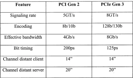
1. Key features of PCIe Gen 2.0 and PCIe gen 3.0 ... 11
2. Comparison of passive CTLE methods ... 20
3. V ia design specification ... 24
4. Port impedance of HFSS simulation models... 36
5. Values of the circuit elements of the CTLE filer ... 41
List of Figures
Page
1. PCIe channel via a backplane ... 12
2. D ifferential Signaling ... 13
3. Effect of cross-talk between channels ... 14
4. Insertion loss of a transmission line 100 mils in length ... 16
5. A sample eye diagram ... 17
6. The eye template for Gen 2.0 PRBS analysis...17
7. The eye template for Gen 3.0 ... 18
8. Decision Feedback Equalization ... 20
9. The interconnect simulation component ... 22
10. Trace specification developed by Mohammad Kermani employee at NetApp ... 23
11. T race 3D m odel ... 24
12. Differential Impedance calculator ... 26
13. Gen 2.0 and Gen 3.0 simulated channel topology ... 28
14. Gen 2.0 eye and Gen 2.0 channel under Gen 3.0 speed ... 29
15. FIR filter ... 30
16. Transmitter waveform with de-emphasis and pre-shoot ... 30
17. Circuit diagram of the CTLE filter ... 31
18. Channel equalization and de-emphasis optimization process ... 33
19. Decision Feedback Equalization process ... 34
20. The effect of board material on the signal quality with eye mask for Gen 2.0 ... 37
21. Via with and without backdrilling ... 38
Page
22. Effect of backdrilling of the via ... 38
23. E ffect of via stub length ... 39
24. Bode plot of the CTLE filter ... 41
25. Eye diagram at the receiver end with CTLE filtering ... 43
26. Eye diagram at the receiver end with DFE ... 44
27. DFE eye closure probability ... 44
1. Introduction
Band limited wire-line interconnects can be found in various high-performance digital
systems - from backplanes of high-speed internet routers, to server/rack backplanes in
data-centers, to processor-memory interfaces in modem portable and desktop computers. All these devices are limited by the same channel issues (dielectric and skin loss, connector cross-talk and impedance discontinuities) as they try to reach high data rates. Various equalization techniques can be utilized to reduce these issues. This thesis attempts to do so by designing and simulating a PCIe communication channel, which fulfills the PCIe Gen 3.0 preliminary specifications that require a 8Gb/s data rate.
Chapter 1 will address the background, motivation and problem statement and the objectives of the thesis. Chapter 2 will outline the theoretical knowledge that is required for this thesis work. The method of implementation is highlighted under Chapter 3. Chapter 4 specifies the resources necessary to complete this project and Chapter 5 presents the simulation results. The results of the simulation will be discussed under Chapter 6 and possible future enhancements
are detailed under Chapter 7.
1.1. Background
PCI Express (PCIe) is the third generation of multi-purpose I/O interface that was
introduced by the PCI Special Interest Group (PCI-SIG) since its inception in 1992 [6]. This organization was established to develop and manage the PCI standards. In 1994 PCI-SIG introduced PCI (Peripheral Component Interconnect), later known as Conventional PCI, as its first architecture. Second introduction by PCI-SIG enhanced the performance of PCI to PCI Extended (PCI-X). PCI-X is a high performance variant of 64-bit PCI design.
In 2004 the PCIe standard was introduced by the PCI-SIG organization. This interface can be used across the computing industry from mobile through high-end servers and even communication equipment. PCIe allows each device to have its own dedicated link. Each link comprises of one-way point to point lanes. A lane contains a Transmit and a Receive with a low voltage differential signal. Two generations were introduced under the PCIe architecture. PCIe Gen 1.0, and PCIe Gen 2.0. Each generation has data transmission rates of 2.5 Gb/s and 5Gb/s respectively. Under the PCIe architecture, each generation achieves greater bandwidth by doubling the data rates [2].
1.2.Motivation & Problem Statement
A new generation of PCIe architecture; Generation 3.0 is underway to double the
bandwidth to 8GT/s under the 128/130 scrambling coding system. Due to this new scrambling code, the transition from 5GT/s to 8GT/s is highly desirable since it results in an increase in the data rate without doubling the signal rate. Furthermore, under the PCIe preliminary specifications presented by the PCI-SIG organization, PCIe Gen 3.0 attempts to reduce latency and have greater power management capabilities compared to its predecessors. This new technology is desirable in a backplane environment as in the case of this thesis, since increase throughput and/or use of fewer lanes results in lower power requirement and increase throughput.
As with all new technologies, there are some key challenges engineers must face in order to transition from PCIe Gen 2.0 to PCIe Gen 3.0. Some key features of the PCIe Gen 2.0 and PCIe Gen 3.0 are given in table 1 [4].
Table 1: Key feature of PCIe Gen 2 and PCIe.Gen 3
The key challenge of this architecture is to accommodate twice the signaling rate while maintain lower clock timing and jitter tolerance. According to the Gen 3.0 specifications, the receiver end is a closed eye [13]. In a backplane environment as in the case of this thesis, more complex equalizer techniques at the Transmitter and Receiver end, and better jitter management techniques are required to obtain the desired eye opening. Another key challenge faced while working on this thesis was that PCI-SIG is still in the process of producing final design specification for PCIe Gen3. Hence driver and receiver models which are specifically compatible with PCIe Gen 3 speeds were not readily available.
1.3. Objective
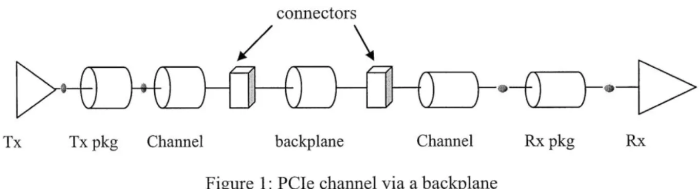
The overall objective of this thesis was to develop a model to simulate a PCIe channel connecting two controller boards via a backplane. This channel must meet the specifications of the PCIe Gen 3.0 standard. Figure 1 shows this system of interest.
Feature PCI Gen 2 PCIe Gen 3
Signaling rate 5GT/s 8GT/s
Encoding 8b/10b 128b/130b
Effective bandwidth 4Gb/s 8Gb/s
Bit timing 200ps 12 5ps
Channel distant client 14" 14"
connectors
Tx Tx pkg Channel backplane Channel Rx pkg Rx
Figure 1: PCIe channel via a backplane
As part of the thesis work various board material, via breakouts and backdrilling of the vias were explored. Furthermore, de-emphasis techniques at the transmitter and receiver equalizer techniques were explored to obtain a model that functions favorably under PCIe Gen 3 speeds.
As part of the thesis work the following channel criteria were also explored:
e De-emphasis technique at the transmitter
" Behavior of the channel under different board materials and back drilling of the vias
* Behavior of the channel under different receiver equalizer techniques
" Channel lengths
2. Theoretical Basis
As part of the thesis work it was imperative to have a thorough understanding of signal integrity issues such as, cross-talk and reflection loss, frequency and time domain analysis and PCIe design principles while designing high speed communication channels. Furthermore, it was important to obtain an understanding of channel measurement techniques and various signal enhancement techniques in order to develop a working model of a particular channel. The
following section describes such topics to provide the reader with the necessary theoretical background to better understand this thesis.
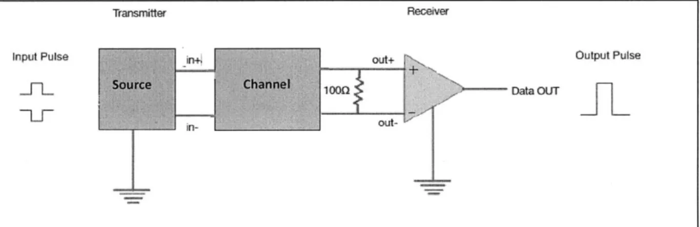
2.1. Differential Transmission Lines:
Differential transmission lines are made of two single ended traces on which a complementary voltage is applied [16]. The advantage of this signaling method as opposed to a single trace is its ability to reject external common-mode interference (noise), as well as provide a tight current return path for differential mode. Since both lines will experience the same noise, subtracting one line voltage from the other line voltage, will result in noise cancelation. The second advantage to this method is that less amount of power is used in differential traces, as opposed to single ended traces to send the same signal. This is due to the fact that differential signal contains its own reference voltage that allows for much smaller swing. This ability to have small voltage swing allows for less power consumption.
Transmitter Receiver
Input Pulse out+ Output Pulse
Figure 100 Data ouT
2.2. Signal Integrity issues:
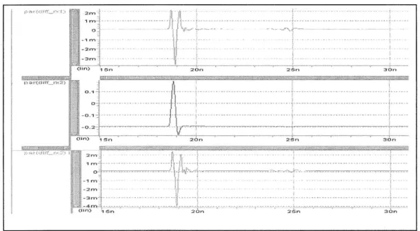
There are many signal integrity issues that Printed Circuit Board (PCB) design engineers need to consider when designing high speed channels. An important signal integrity issue is cross-talk, which arises when there is undesirable inductive or capacitive coupling between channels. For instance, if one channel is carrying a signal and there is a nearby passive channel, a small voltage is generated in this passive channel due to change in electrical and magnetic fields [21].
The following Figure 3 depicts a signal pulse travelling down a channel shown in the middle and the voltages generated due to cross-talk on the channels on either side of this carrier. It is important to note that the pulse amplitudes on the two victim lines (shown on the top and bottom graphs) are significantly smaller than the pulse amplitude on the aggressor line.
) 15 20n 25n 3on
o~0 - - ---
Another signal integrity issue is date-dependent jitter (DDJ). DDJ is the variation in the transition time between symbols. This is caused due to Inter Symbol Interference (ISI). ISI is the result of sending high data rates down low-bandwidth material such as copper wires [3].
Two other important signal integrity issues are return loss and insertion loss of a signal. When a trace connects to cap or a via on a PCB, a signal may encounter changes in impedance. Due to these differences in impedance part of the signal may bounce back to the transmitter. This is called return loss. Return loss can be calculated by using the following equation 1.
RL (dB) = 10 log 0 PT Equation 1
PT is the power transmitted by the source and PR is the power reflected.
Insertion loss is the loss of the signal power as the signal travels down a transmission line or any conducting object. Insertion loss occurs due to the difference in impedances down a conducting channel and also due to skin effect and dielectric losses of the material. It can be calculated by using the following equation 2.
IL(dB) = 10 logo PR Equation 2 'Pr
PT is the power transmitted by the source and PR is the power received.
The following Figure 4 shows the insertion loss experienced by a transmission line 100mil in length with FR408HR material.
Figure 4: Insertion loss of a transmission line I 00mils in length- linear scale.
2.3.Signal quality:
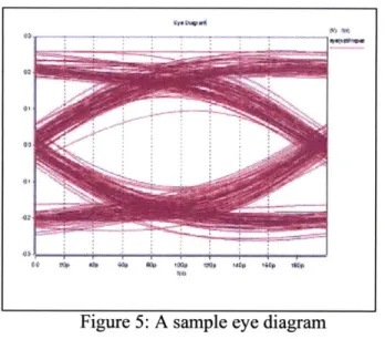
There are several methods to describe the quality of a signal travelling through a channel. One such method is the use of eye diagrams. An eye diagram is generated by transmitting a bit stream pattern that represents all possible bit stream patterns through the channel to be tested. Each received cycle is overlaid on the previous cycle to superimpose all the cycles. This superimposed waveform is in the shape of an open eye, hence the name eye diagrams [18]. By measuring the width of an eye and the height of an eye (measuring the eye opening) with the use of an eye mask we can determine whether a particular channel is compliant with PCIe
V 7
Figure 5: A sample eye diagram
The eye masks for Intel Pseudo Random Bit Stream Analysis (PRBS) for Gen 2.0 is given under Figure 6 [11].
Figure 6: The eye template for Gen 2.0 PRBS analysis Iw
<V Di f PP
X1 YX2
Figure 7: The eye template for Gen 3.0
The Figure 7 above depicts the PCIe Gen 3.0 eye template provided in the PCIe Base Specification Rev. 03 V 0.7 [13] by PCI-SIG organization for a receiver eye after CTLE in FR4 material.
Another method to measure the quality of a channel is to measure the channel's scattering parameters. Scattering parameters includes return loss measurements (S 11) and insertion loss measurements (S21) of the channel.
2.4. Enhancement of the Signal Quality:
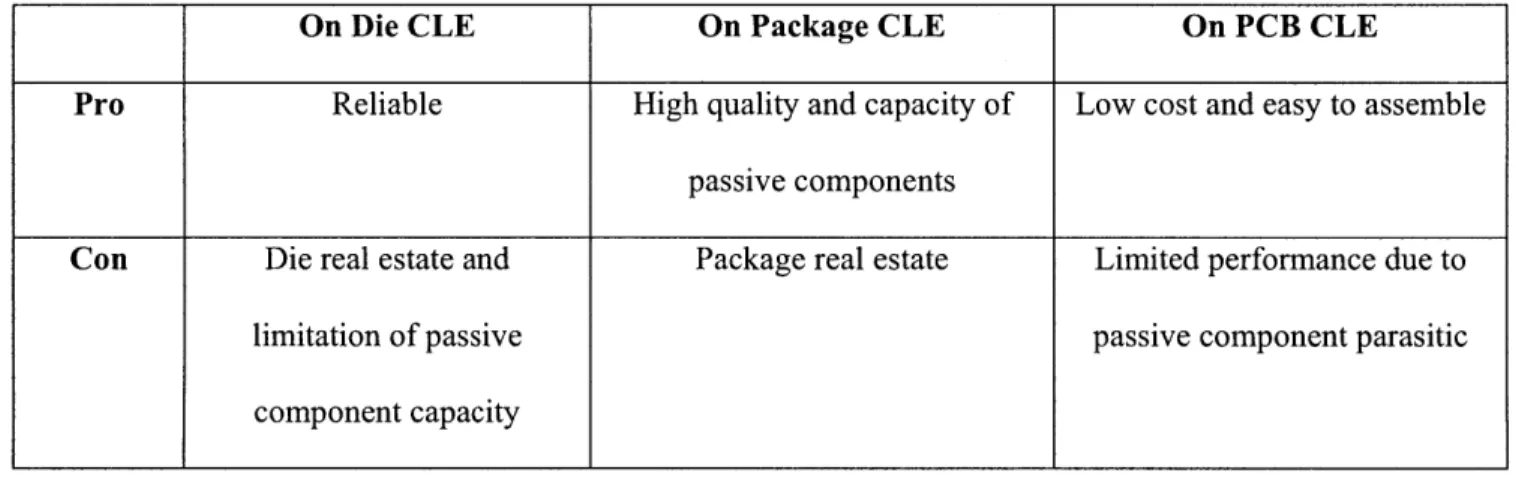
As previously highlighted there are various signal integrity issues an engineer must consider when designing a high speed communication channel. Due to the high data rate of PCIe Gen 3.0, it is expected to have a closed eye at the receiver end of the channel. To widen this eye, Continuous Time Linear Equalization (CTLE) technique was suggested under the guidelines of the version 0.7 of the specifications [13]. Equalization is a procedure used to compensate for non-ideal channel characteristics by equalizing the frequency spectrum. As mentioned earlier, the use of low bandwidth material such as copper wires and PCB traces to process high data rates generates ISI. CTLE can be used as a method to counteract this bandwidth limitation. CTLE is a high pass / low pass filter configuration which is designed in the frequency domain. CTLE can be done actively or passively. Active CTLE can be more reliable and tunable; however, it will require high power and cause latency. Passive CTLE is non tunable yet causes less latency. For this thesis, passive CTLE implementation was used due to reduced latency and lower power requirement.
Passive CTLE can be implemented in three different ways: On die, on package or on PCB. In the thesis we used transmitter and receiver models from outside vendors. Therefore the only method available to implement CTLE is the PCB implementation. Nevertheless, a comparison of the three implementation method described by the Qualcomm Digital Signal Integrity presentation is given below under table 2 [24].
Table 2: Comparison of Passive CTLE methods
Another equalization method is Decision Feedback Equalization (DFE), which, unlike linear equalization techniques, removes the ISI with minimal noise amplification or signal attenuation [3], Decision Feedback Equalization alters the frequency response of the equalizer to remove ISI generated by the channel at the receiver end. This non-linear equalizer performs its task by using previously made decisions to eliminate ISI on the current signal modulation. The following Figure 8 depicts a simple DFE system.
Figure 8: Decision Feedback Equalizer.
On Die CLE On Package CLE On PCB CLE
Pro Reliable High quality and capacity of Low cost and easy to assemble
passive components
Con Die real estate and Package real estate Limited performance due to
limitation of passive passive component parasitic
3. Technical Approach
To achieve the desired goal of developing a PCLe Gen 3.0 channel, several tasks were performed. These tasks are described as follows:
3.1.
Integrated Circuit Manufacturer's HSPICE model:
The integrated circuit manufacturer's model is a readily available HSPICE simulation model which depicts various topologies that connect two cards across a backplane. The basic interconnect topology of the simulation given under this model is depicted in the Figure 9 below. The red boxes depict the models directly provided by the integrated circuit manufacturer. The blue boxes represent the connector models provided by an external manufacturer. The green boxes depict the model created specifically for this thesis.
.. ..... ..... .. ... .... .. .- . . .. . ... . . ..._ . . . . .. ..... ....
Bit Drive Sub-circuit Transmitter Buffer on Die
Package Sub-circuit Via Sub-circuit ViaSu-ict AC Linking Capacitor Baseor otn Via Sub-circuit Via Sbdci 1/0 Board Routing Package Sub-circuit Receiver Buffer on Die
Figure 9: The interconnect simulation component
These simulation models were used to understand how to create HSPICE models which can replicate physical systems that connect two controller cards via a backplane. In the HSPICE simulations, the transmitter can be excited by either a Pseudo Random Bit Stream (PRBS), a Card Electromechanical (CEM) bit pattern or a Peak Distortion Analysis (PDA) data pattern. The HSPICE programs were thoroughly read and various simulations were run on them to understand how each component interacts with each other. After each simulation the data was analyzed in eye diagram format and evaluated against the PCIe Gen 2.0 specifications [11]. For the purpose of this thesis and due to time constraints, only PRBS analysis was performed for the spice simulations and PDA analysis was used to estimate the worst case eye opening in MATLAB.
3.2. Gen 2.0 trace and via models:
Since the system used in the company is different from the model presented under Integrated circuit manufacturer's chipset, new simulation models for the traces, vias, and the connectors were created. This is mainly due to the different stack layout of the PCBs and the different specifications used for routing. To create these models Ansoft HFSS and Ansoft Via Wizard was used.
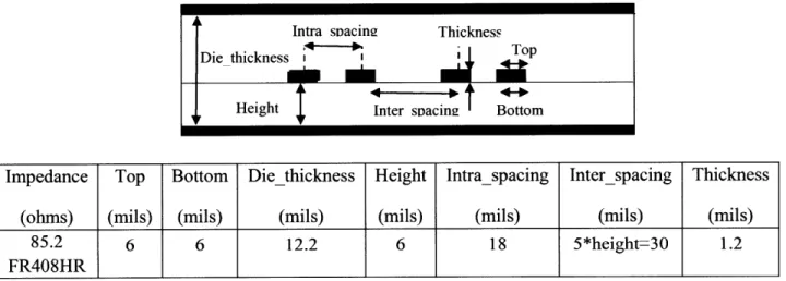
To create the required models certain pre-defined specifications were used. These specifications were developed by another colleague, Mohammad Kermani, from NetApp, Inc. The trace specifications are depicted under the Figure 10 below [25].
Impedance Top Bottom Diethickness Height Intra spacing Inter-spacing Thickness
(ohms) (mils) (mils) (mils) (mils) (mils) (mils) (mils)
85.2 6 6 12.2 6 18 5*height=30 1.2
FR408HR
Figure 10: Trace specification developed by Mohammad Kermani, NetApp, Inc.
The trace model was created using Ansoft HFSS. It is a 3D model with three differential pairs depicting two aggressor lines with a victim line in the middle. The cross section of the 3D model was shown in the Figure 10, where the trace width, trace thickness, trace spacing and die thickness were specified. The dielectric material used for the stack up was FR408HR with
Intra sDacine Thickness
Die thickness Top
permittivity of 3.75 and loss tangent of 0.01. The FR4 material has a permittivity of 4.4 and a loss tangent of 0.021. The impedance of the trace model was designed to be 85.2 in order to match the impedance of the connector model, which was 85U. The Figure 11 below shows the
3D model of the trace model.
Figure 11: Trace 3D model
Via models which connect the created using the HFSS software and following table 3 [25].
traces from
Via Wizard
one layer to another layer on the PCB was
3.0. The via specifications are given in the
Table 3: Via design specifications
Via Type Pitch Size Diameter Pad Size Anti-Pad Size
IOXM board via at connector 55.1 mils 23.6 mils 36 mils 58 mils
IOXM board via at capacitor Imm 12 mils 20 mils 25 mils
Backplane via at connector 55.1 mils 23.6 mils 36 mils 58 mils
After each model was created, they were individually tested using HFSS analysis tool. Ansoft HFSS performs frequency domain analysis by first creating an adaptive mesh that conforms to the electrical performance of the device. Once an accurate mesh has been created, the HFSS uses this mesh to perform a desired frequency sweep. Generally this adaptive meshing is performed on the maximum frequency of the desired frequency range. For further details of
this process, please refer to the HFSS manual mentioned under references [9].
An interpolating frequency analysis of the traces and vias were conducted ranging from 0 GHz to 20 GHz with a linear step size of 0.02 GHz. Interpolating sweep analysis solves at
discrete frequency points that are fit by interpolation. The frequency range and frequency step size was determined by first selecting the time domain simulation window and then determining the appropriate frequency range. The following equations 3 and 4 depict the relationship between time domain analysis and frequency domain analysis.
Maximum simulation time = Equation 3
Frequency step
1
Time step = Maximum simulation Frequency Equation 4
According to the frequency domain values mentioned above, the time domain analysis would range from Ons to 50ns in 50ps steps. Since this step size is not appropriate to analyze data rates of 5Gbps and 8Gbps, a step size of 2ps was selected. This time step indicates the maximum frequency to be 500GHz. Since signal loss beyond 20GHz is quite significant, the HFSS
frequency sweeps were only performed up to 20GHz.
The generated Z matrix was analyzed to determine whether the correct differential
calculated using a differential impedance calculator available online on the "Ideas Consulting" website [17]. This online calculator is designed for a differential stripline model where the user can input the trace width, thickness, spacing, distance between the planes and the relative dielectric constant. The following diagram 12 displays the web interface of this calculator.
Differential Stripline Impedance Calculator
Notes:
1) Calculation assumes traces are centered vertically.
2) SIT > 5.0
Enter dimensions:
Trace width (W) mils Trace thickness (T) mils Trace spacing (S) mils Distance between planes (B) mils
Relative Dielectric constant (Er):, Compute Z
Differential Trace Impedance ohms
Figure 12: Differential impedance calculator
Another validation method was to graph the insertion loss and return loss of each model. These graphs were used to ensure that the traces functioned as expected.
3.3.
Integration of HSPICE file with HFSS models:
The trace and via models were created using Ansoft HFSS. However, the entire Gen 2 system was simulated using the HSPICE simulation software. Therefore, the new HFSS models were integrated into the HSPICE model prior to simulation.
The trace model's resistance, impedance, conductance and capacitance (RLGC) data was extracted in a tabular format. This table file (.TAB file) was incorporated into HSPICE using the w-element syntax [Appendix - 3]. The reason for selecting this technique is because it is
straightforward and because of its ease of implementation in HSPICE.
Via's scattering parameter data was extracted by using the touchstone file format. It was summoned within HSPICE as an S-element [Appendix - 4].
3.4.
Simulation of the new Gen 2 model
The simulation of the new system in HSPICE was conducted in several stages. The first stage was to test each trace model individually in HSPICE, generate the transfer functions of the model and compare them to the HFSS transfer function.
The second stage comprised of incorporating the via models one by one into the HSPICE model and running the simulation under PRBS bit pattern
Finally the overall system was simulated up to 50 ns time interval (derived under section
3.2 equation 3) with all the vias, trace models and vendor specific connector models to imitate
the system designed by the company. The IOXM board which is an 10 expander board [Appendix - 2] has 14 layers on the stackup and the backplane stackup [Appendix - 1] contains 18 layers. The following Figure 13 displays a channel topology used for Gen 2.0 and Gen 3.0
Rx
Figure 13: Simulated Gen 2.0 and Gen 3.0 channel topology
3.5.
Identify changes to Gen 2 model for Gen 3 requirements
As mentioned under the introduction the main difference between the PCIe Gen 2.0 and Gen 3.0 is the speed of data transmission. In Gen 3.0 we attempt to transmit data at 8Gbp/s. To understand why any design changes are required to switch from Gen 2.0 speeds to Gen 3.0
Tx
Trace LTx1 LTx2 LMP LRx
Length 2" 2" 15" 4"
speeds, the Gen 2.0 model was simulated at Gen 3.0 speeds. The eye diagrams of the Gen 2.0 channel made of FR408HR material with backplane channel length of 15" and the same Gen 2.0 channel simulated under Gen 3.0 speed are depicted below under Figure 14.
-03
Simulated Gen 2 channel Simulated Gen 2 channel under Gen 3 speed
Figure 14: Gen 2.0 eye and Gen 2.0 channel under Gen 3.0 speed
As shown in the Figure above, the receiver eye under Gen 3.0 speed is far more distorted than the receiver eye of Gen 2.0. The width and the height of the eye are dramatically reduced. At the Gen 3.0 speed the eye height is 20.4 mV and eye width is 35.5 ps. Therefore, it is apparent that some design changes are needed to improve the channel.
3.6. Development of Gen 3 model
There are several channel enhancement suggestions provided by the PCI-SIG organization for PCIe Gen 3.0 channels. The first recommendation is the use of a 3-tap Finite Impulse Response (FIR) filter to provide transmitter equalization as shown in Figure 15 below
[13].
.. . .. ... 1111111111W . - - ..
dm
C-1
VTX = n=I-L(W VTX Cn dM-nFigure 15: FIR filter
The values of the filter coefficients are determined by the transmitter de-emphasis
and the pre-shoot values. De-emphasis is the process of changing the amplitude of the low frequencies or changing the attenuation of the non-transitioning bits. The following Figure 16 depicts a transmitter waveform with de-emphasis and pre-shoot.
coeff=[-0 067 0.667 -0.267:
De-emphasis and pre-shoot can be calculated by using the following equations:
de -emphasis 20 log10 V
pVr
Pre - shoot = 2 0 Ing -'
Equation 5
Equation 6
Once the tap values are determined, the 3-tap FIR filter can be easily implemented by altering the transmitter code found in the integrated circuit manufacturer's chipset. The available code is designed for a 6-tap FIR filter. By setting the first three taps of the filter to our desired values we can implement this equalization technique quite conveniently.
The second recommendation made by PCI-SIG organization is to implement receiver equalization by using a Continuous Time Linear Equalizer (CTLE). The suggested circuit implementation is a high pass/ low pass filter system to enhance the amplitude of the high frequency components of the received signal. The suggested circuit diagram is shown in Figure
17 [10].
C1 -"
> R4
R2 R3
R1 C2
The transfer function of the filter is given below equation 7:
=upu
G+ Equation 7Ed
R E quaon 8 R1+ R-= (IRx)E quation 9 R CEquation 10If we assume that resistor R1 and resistor R2 values are equal then we can
observe that the location of the first pole should be at twice the frequency of the zero location. The resistor R4 is the termination resistance at the receiver end which is 50 0.
3.7.
Simulation & evaluation of Gen 3 model
To develop Gen 3.0 channel we need to determine the FIR tap values for transmitter de-emphasis and the pole locations, gain and zero locations of the CTLE filter for receiver equalization. The FIR tap values can be determined by first obtaining an insertion loss of the channel (S21 parameters) and by extracting the impulse response of the channel from this data. From the impulse response, we can obtain a bit spaced sampled pulse response of the channel by convolving the impulse response with a pulse train. This pulse response is used to generate zero-forcing equalization coefficients for transmitter de-emphasis with peak power limited to 1 [15]. The MATLAB code for this process, developed in this thesis, extends the code initially written
by Prof. Vladimir Stojanovic and students in his Integrated Systems Group at Massachusetts
Once the tap values are determined using the MATLAB code, FIR 3-tap filtering process was implemented by changing the tap values of the Verilog-A code provided by integrated circuit manufacturer's simulation set [Appendix -7]. In the code provided to the user, the transmitter had a 6-tap FIR filter already incorporated into the Verilog-A code. However, for the Gen 2.0 model, four of the taps were set to zero and only two were used which meets the Gen 2 specification [12].
The determination of the pole/zero locations and the gain of the CTLE filter are done by using an optimization method developed as a part of this thesis. Initially the pole/zero locations and the gain of the CTLE will be pre-determined. Channel insertion loss will be filtered by the
CTLE filter and FIR tap values are calculated. This data is used to produce an equalized pulse
sequence by convolving the tap values with the pulse response. The worse-case eye margin is calculated by determining the value of the equalized pulse sequence at the location of the main tap. This process is repeated to maximize the eye margin by changing the location of the poles/zero and the gain of the CTLE filter. The following flow chart under Figure 18 shows this repetitive optimization process.
Channel
Transfer LBit spaced
Function sampled pulse
response
Worst-easeI
eye margin FIR tap
values Equalized
pulse response
As a comparison to the CTLE equalization method, DFE equalization method was
also performed using MATLAB code provided by Prof. Stojanovic [Appendix - 6]. The
following flowchart in Figure 19 shows the Decision Feedback Equalization process.
Channel Transfer Impulse Pulse Response
Function response of the
L Channel
Worst-case Eye DFE Tap Values
Margin
Figure 19: Decision Feedback Equalization process
4. Required Resources
For this thesis topic the following software, hardware and information resources were required:
4.1. Software Resources:
" HSPICE -HSPICE is a device level circuit simulator. HSPICE takes a spice file as input
and produces output describing the requested simulation of the circuit.
. Ansoft HFSS - This simulation software allows users to precisely model and simulate 3D
electromagnetic fields of high speed, high frequency components.
manner. This software tool generated models which are easy to integrate with the Ansoft
HFSS for field simulation.
* MATLAB - MATLAB is a high level language and interactive environment that allows
the user to perform computationally intensive tasks in a fast and efficient manner.
4.2. Hardware Resources:
e Network Analyzer - To perform scattering parameter and channel eye measurements
* Two line cards and backplane.
4.3. Information Resources:
It is important to have some understanding of signal integrity issues when working on this proposed thesis. Several books were read to obtain a clearer understanding of return and insertion losses, jitter tolerance, cross-talk etc [18-22].
5.
Results
Various results were generated throughout the course of the thesis work. These results can be categorized under several groups: The HFSS model analysis, Gen 2.0 HSPICE simulation results, Gen 3.0 transmitter de-emphasis and receiver equalization results. Each section will be presented in detail below.
5.1. HFSS model analysis:
As mentioned under the technical approach of this thesis, HFSS trace and via models were evaluated in frequency domain and the insertion loss and the port impedances were analyzed. The following table 4 displays the port impedance of the simulated model along with the expected port impedances.
Simulation Model Expected Port Simulated Port
Impedance (fl) Impedance (fl)
Differential stripline trace: 6mil wide, FR408HR material 85.2 83.22
Differential capacitor IOXM board via: L1-L3 signal trace, FR408HR 85.2 84.64
Differential connector IOXM board via: Ll-L3 signal trace, FR408HR 85.2 84.73
Differential connector backplane via: L1-L3 signal trace, FR408HR 95.9 91.67
Differential capacitor IOXM board via: L1-L12 signal trace, FR408HR 85.2 84.75
Differential connector IOXM board via: L1-L12 signal trace, FR408HR 85.2 84.65
Table 4: Port impedances of HFSS simulation models
Analyzing the insertion loss of the HFSS trace models for a frequency range of OGHz
-20GHz with a trace length of 100 mils indicates that the insertion loss at 4GHz is 0.0611 dB for FR408HR material and 0.1297 dB for FR4 material. The insertion loss is more than double for the FR4 dielectric.
5.2.
Gen 2.0 HSPICE simulation results:
Simulations for Gen 2.0 model were performed to test several design parameters: board material, via backdrilling, via breakout. These results are listed below.
e Board material: The simulations were performed using two different board materials; FR408HR and FR4. The dielectric constant of the FR408HR is 3.75 with a loss tangent of 0.01. The dielectric constant of FR4 is 4.4 with a loss tangent of 0.021. The Figure 20 depicts the eye diagrams of a 23" channel made with these two different board materials.
Figure 20: The effect of board material on the signal quality with eye mask for Gen 2.0. (a) The receiver eye pattern of FR408HR board material and (b) The receiver eye pattern of FR4 board
material
o Via backdrilling: Backdrilling is the process of removing a part of the via stub to enhance the signal quality. The Figure 21 depicts a cross section of the via with backdrilling and without backdrilling.
Figure 21: Via with and without backdrilling
Figure 22 shows the insertion loss of a interface with backdrilling of the vias on the backplane and one without backdrilling of the vias on the backplane for a 15" channel on the backplane made of FR408HR material.
Figure 22: Effect of back drilling of the vias.
Note the significant at 4GHz and 7GHz on the channel without backdrilling. -tyn jGHZ]
* Via breakout: The layer on which the signal travels can have an effect on the signal quality, especially if there are vias on the path of the trace. This is due to the fact that the via stub will be greater if the signal trace is on a higher layer than at the bottom layer of the stackup. Simulations were performed to analyze which signal layer on the IOXM board and the backplane corresponds to the best signal quality. The following Figure 23 depicts the receiver eyes of two channels with 15" on the backplane made of FR408HR material. The first channel has the signal on layer 3 throughout the channel. The second channel has the signal trace on layer 12 on the IOXM board and layer 3 on the backplane.
Eye at the receiver at layer 3 throughout Eye at the receiver at layer 12 on the backplane
Figure 23: Effect of via stub length
5.3.
Gen 3.0 Transmitter de-emphasis and Receiver equalization results:
The starting point of the pole/zero locations and gain of the CTLE filter was determined
by first understanding that we require a high pass filter around our frequency of interest, which is
4GHz. By observing the CTLE filter suggested by PCI-SIG mentioned under the technical
approach of this thesis, the zero should occur prior to 4GHz, the first pole should occur around 4GHz and the second pole should be located after 4GHz. The gain can be determined by observing the S21 parameter of the channel. Based on these deductions, the pole and zero locations and the gain of the CTLE filter were first determined to be at:
Zero =1GHz;
Pole 1 = 2GHz;
Pole2 = 8GHz;
Gain = 0.5
The MATLAB [Appendix -5] was run with these initial values. Then the code execution was repeated to optimize the eye margin. The final results yielded the worst-case eye margin of 10.4mV for the following variable values:
Zero = 0.64 GHz
Pole 1 = 4.9 GHz Pole 2 = 14.7 GHz
Gain = 3/22
Bode Diagram
-901- 1 1 . . - I . I I , - ,1
-1"1*10 to 10"1 10" 10"
Frequency (rad/sec)
Figure 24: Bode plot of the CTLE filter
The Figure 24 shows the magnitude and the phase values of the CTLE filter. The standard values of circuit elements were calculated using the CTLE pole, zero and gain information. These values are given under table 5 below.
0 -10 9 -20 30 -40 45 0
Element name Standard Value Tolerance
Cl 39 pF +/-10%
C2 10 pF +/-10%
RI 6.8Q +1-5%
R2 1.02 +1-5%
Table 5: Values of the circuit elements of the CTLE filter
By applying these values, the first pole is located at 4.681 GHz and the second pole is
located at 14.4 GHz and the zero is located at 0.60013 GHz. A worst-case eye margin of 10.OmV can be obtained by applying a CTLE filter with the above component values. Further analysis was performed to calculate the worst-case eye margin when the component values vary according to their tolerance. Table 6 below highlights this data.
Element Name Tolerance Worst Case Eye Marin
C1 +10% 8.9 mV -10% 8.7 mV C2 +10% 9.4 mV -10% 8.8 mV RI +5% 8.0 mV -5% 10 mV R2 +5% 9.1 mV -5% 9.1 mV R3 +5% 9.7 mV -5% 8.4 mV
Table 6: Worst-case eye margin with the component tolerance
The Figure 25 below depicts the receiver eye for a 23" channel with 15" on the backplane made from FR408HR material. This Figure contains the receiver eye generated using the MATLAB code with the newly derived FIR tap values at the transmitter end.
eye diagram. 1/Tsym is 8G.
0 10 20 30
Time (*5e-1 2)
40 50 60
Figure 25: Eye diagram at the receiver end with CTLE filtering
The Decision Feedback equalization technique yielded a worst-case eye height of 67.3 mV for the input channel transfer function. The DFE tap values were -0.1925, 0.6223, and
-0.1853. The eye diagram of the simulation is depicted in Figure 26 and the DFE eye closure
probability is depicted in Figure 27.
0. 0.1 0. 0.0 -0.0 -0. -0.1 2 5 5-21 ... ... :: ::: .. ... .... .... ... ... .. ... ...
eye diagram. 1/Tsym is 8G. 0.4 0.3 said& 0.2 0.1 0) 0 . -02
M
1111:
-0.32Ht~I
~li-0..
-0.4, 0 10 20 30 40 50 60 Time (*5e-12)Figure 26: Eye diagram at the receiver end with DFE
-5. -20 -.. 10 -1. - . -. so1.1. CmV .0 . . . . 0l -1 . ... - 2 . .. . .. . -25-I -200 -150 -100 -50 0 50 100 150 200 mV
Figure 27: DFE eye closure probability
6. Discussion
The goal of this thesis was to design and simulate a PCIe Gen 3.0 communication channel. Several key lessons and observations were made in the process of developing simulation models of traces and vias and simulating them in HSPICE to achieve this end goal. Some of these key lessons will be discussed under this section.
The first observation is that the accuracy of the HFSS models is critical to generating a valid communication channel. It is imperative to select a valid range for frequency analysis in
HFSS which relates to the time domain simulation the user intends to run in HSPICE. The HSPICE results are invalidated if the frequency sweeps of the HFSS models are chosen
incorrectly because there is not a valid transformation from frequency domain to time domain.
The second observation is that the mode of data extraction from HFSS into HSPICE can influence the final result. In this thesis the trace models were incorporated into HSPICE as w-elements and via models were incorporated as S-w-elements.
The third observation is that it is important to select the right settings for the driver model in HSPICE. By selecting incorrect de-emphasis values or power values, the end result will be incorrect.
From the simulation results of Gen 2.0 several design guidelines can be made which can predict the behavior of the Gen 3.0 channel. From the results we can observe that the board material used during design stage can affect the overall length of the channel. By using the FR408HR material we can effortlessly meet the eye mask for a 15" long channel on the
backplane. However, if we use FR4 material, the 15" channel fails the eye mask test for Gen 2.0.
By using FR4 material we were only able to reach a channel length of 10" on the backplane. The
reason for this difference is due to the dielectric loss of the material. FR408HR has a smaller dielectric loss compared to FR4 material. Therefore it results in having an insertion loss which is approximately half the insertion loss of the FR4 material.
The second observation one can make from the simulation results is that backdrilling of the via stub can affect the signal amplitude. Since long via stubs means reflection loss due to stub capacitance, this observation is not too surprising. As seen by the insertion loss of the system shown in Figure 19 on page 33, the presence of notches in the frequency domain indicates more losses due to this stub capacitance.
From the results, it can be seen that the via breakouts determine the via lengths and stub capacitance. This can also affect the signal quality through the channel. It was observed that signal trace on layer 12 on the IOXM board and the signal trace on layer 3 with backdrilling on the backplane results in maximum eye height.
The MATLAB analysis on the Gen 3.0 channel was performed to determine the
FIR tap values and the appropriate CTLE coefficients. The precursor and main tap values
(-0.1007 and 0.7278 respectively) were within the range specified by the PCI-SIG organization.
However the post curser tap value of 0.1715 was not within the 0 to -0.35 range specified by
PCI-SIG. One possible reason for this is that the CTLE amplifies most of the high frequency
components. Therefore the transmitter tap values are not typical pre-emphasis values. Another reason for this is that the S21 parameters of the channel depicted a very high loss in the high frequency range. This loss is mainly due to the loss incurred by the connector model used in this
channel .The following Figure 28 shows a 15" backplane channel made with FR408HR material with and without the connector models. The CTLE coefficients denote a filter that shows high pass behavior around the 4GHz frequency value.
-20 -40 -60 -100 th connectors -12D -IAA 06 2 4 6 8 10 fr*qInCY GHO 12 14 46 1i 20
Figure 28: Effect of the connector model
The decision feedback equalization generated a worst-case eye margin of 67.3 mV, far greater than the minimum required height of 1 OmV. The tap precursor and post-cursor tap values were both within the expected margin of 0 to -0.25 and 0 to -0.35 given by the PCI-SIG organization. Hence DFE is the most optimum mode of equalization for this channel. However, unlike CTLE, DFE does not provide the ease of implementation.
7.
Conclusion & Future Work
In this thesis, a high speed communication channel which meets the eye requirements of the PCIe Gen 3.0 standard was designed and simulated. A Gen 2.0 system was modified to function under the new Gen 3.0 speeds. Several design parameters were evaluated for the Gen 2.0 model. It was determined that using FR408HR board material as opposed to FR4 material improves the signal quality of the channel. Furthermore, it was observed that backdrlling of the via stub can improve the signal quality. The optimum via breakout was observed to have the signal trace on layer 12 on the IOXM board (backdilling depth of 85.38 mil) and on layer 3 on the backplane (backdilling depth of 19.23 mil).
While we have achieved the goal of this thesis which is to design and simulate a PCIe Gen 3.0 channel, several additions can be made to improve the performance of the model. In this work we were not able to use transmitter, receiver and connector models that were specifically designed for PCIe Gen 3.0 standards. The reason for this is that these models were not readily available in the industry at the time of this thesis work since the PCIe Gen 3.0 standards are still under development. It would greatly enhance the model if we include these models in the future and observe the functionality of the channel.
Another enhancement we can make to this model is to incorporate better receiver equalization techniques such Decision Feedback Equalization (DFE). The CTLE equalization method which is currently used in the model is a very basic equalization technique which relies on the designer to determine its pole and zero locations. By incorporating better equalization techniques we have demonstrated that we can obtain a higher worst-case eye opening of 67.3
8. References
[1] J. Boh, "Signal integrity simulation of PCI Express Gen 2 channel," XrossTalk Magazine, pp. 16-20, January 2009.
[2] M. J. Chong, "A PCI Express to PCIX Bridge optimized for performance and area." Master's Thesis, Massachusetts Institute of Technology, 2004.
[3] Al-Dhahir, N.; Cioffi, J.M.; , "MMSE decision-feedback equalizers: finite-length
results," Information Theory, IEEE Transactions on , vol.41, no.4, pp.9 61-975, Jul 1995
[4] J. Pavlat, "PCI Express Gen2/Gen3 update: An interview with Jasmin Ajnovic and Kevien W. Bross, Intel." April 2009.
http://www.compactpcisystems.com/articles/id/?3103.
[5] A. Kazmi, "PCI Express Gen 3 simplified." February 2009.
http://embeddeddsp.embedded.com/design/testissue/214502580;jsessionid=E1CLPQC4I
OMZUQSNDLPCKHSCJUNN2JVN?pgno=1
[6] "About PCI-SIG." 2009. http://www.pcisig.com/membership/aboutus [7] Synopsys, "HSPICE Signal Integrity Guide." March 2005.
[8] Synopsys, "HSPICE RF Manual." September 2005.
[9] Ansoft, "User's Guide - High Frequency Structure Simulator." 2005.
[10] J. Morrison, G. Talbot, "PCI Express 3.0 Electrical." PCI-SIG Developer Conference, 2009.
[11] PCI-SIG, "PCI Express Base Specification Revision 2.0." December 2006.
[12] PCI-SIG, "PCI Express Card Electromechanical Specification Revision 2.0." April
mV. By using this equalization technique instead of passive CTLE, we can obtain longer channel lengths.
Finally, another design variation to explore is to observe the effect of the trace width on the signal quality. By increasing the width of the trace we can reduce the loss in the channel. However this will create routing problems and cross-talk issues. Therefore it is worthwhile to
[13] PCI-SIG, "PCI Express Base Specification Revision 3.0 Version 0.7." October 2009. [14] Keven R. Andryc, "A novel approach to PCI simulation using ScriptSIM." Master's
Thesis, University of Massachusetts Amherst, May 2008.
[15] Sanquan Song, Vladimir Stojanovi, "Behavioral Simulation of a High-Speed Link
Transceiver Using VppSim." July 2008.
[16] "Differential Signaling." November 2009.
http://en.wikipedia.org/wiki/Differential-signaling
[17] Idea Consulting, "Differential Stripline Impedance Calculator." 1999.
http://www.ideaconsulting.com/dstrip.htm
[18] E. Bogatin, "Signal Integrity Simplified." Prentice Hall, 2003.
[19] H. Johnson, M. Graham, "High- Speed Signal Propagation: Advanced Black Magic."
Prentice Hall, 2003.
[20] H. Johnson, M. Graham "High-Speed Digital Design: A Handbook of Black Magic." Prentice Hall, 1993.
[21] D. Brooks, "Signal Integrity Issues and Printed Circuit Board Design." Prentice Hall, 2003.
[22] E. C. Ifeachor, B.W. Jervis, "Digital Signal Processing." Prentice Hall, 2001.
[23] "Common Resistor and Capacitor values for Electronic Circuits." April 2010.
http://www.kennethkuhn.com/students/rlcvalues.pdf
[24] T. Michalka, "Digital Signal Integrity Technical & Non-Technical Considerations."
Qualcomm, April 2008.
[25] M. Kermani, "Pre-layout Simulaions: PCIe Gen. 2 Interconnect with 2 Connectors."
9. Appendix
[11 Backplane PCB layout
Copper Layer Type Weight L 1 Signal 0.Soz
L 3sianissemis/ L 2 Power/ Ground 1.0oz L 3 Signal 1.0oz
L 4 Power f Ground 1.0az L Signal 10oz
L 6 Power / Ground 1.oz L7 Signal 1.0oz.
18 Power!f Ground 2.Ooz L19 Power f Ground 2.0oz
L9 5 Power /Ground 2.0oz 101 Power!/ Grouncd 2.0oz
L12 Signal 1.Ooz
L13 Power ! Ground 1.Ooz
1148 Signal Groade
116 Signal 1.Doz
117 Power!/ Ground 1 .Ooz
116 Signal 10 Sz Orignal Thk 0.67 4.10 DK Fkished Thk (ML) Material hifomation Jada HTE 1/2 oz 0 67mil 23in 3.64 3 98 Isola FR408HR 2113 55% 50in x 125yds
10.00 4.07 1.20 Isola FR408HR 0.25 mm 111 0"X0"(1OmIl) RTF 2x1652 1.20
Isola FR40HR 2113 55% 50in x 125yds Isola FR408Hr 2113 55% 50in x1 25yds 13.20 3.82 12.18 Isola FR408HR 2116 53% 50In x 125yds
10.00 4.07 1.20 Isola FR408HR 0.25 mm 111 0"XO(10mil) RTF 2x1 652 1 20
Isola FR408HR 2113 55% 50in x 125yds Isola FR408HR 2113 55% 50in x 125yds 13.20 3.82 12.18 Isola FR408HR 2116 53% 50in x 125yds
10.00 4.07 1.20 Isola FR408HR 0.25 mm 111 1"X0"(10mil) RTF 2x1652 1 20
Isola FR408HR 2113 55% 50in x 1 25yds Isola FR408HR2113 55% 50in x 125yds 13.20 3.82 12.06 Isola FR408HR 2116 53% 50in x1 25yds
5.00 3.71 2.40 Isola FR408HR 0.127 mm 2!2 0"X0(5mil) 21 080 240 Isola FR408HR 2113 55% 50n x 1 25yds 8.20 3.86 7.72 Isola FR408HR 2113 55% 50l x 125yds 5.00 3.71 2.40 Isola FR408HR 0.127 mm 2/2 0"X0"(5mil) 21 080 2.40
Isola FR408HR 2116 53% 50in x 1 25yds Isola FR408HR 2113 55% 50in x 125yds 13.20 3.82 12.06 Isola FR408HR 2113 55% 50in x 125yds
10.00 4.07 1.20 Isola FR408HR 0.25 mm 111 0"XO"(1Omil) RTF 2x1652 1.20
Isola FR408HR 2116 53% 50in x 125yds Isola FR408HR 2113 55% 50in x 1 25yds 1320 3.82 12.18 Isola FR408HR 2113 55% 50in x1 25yds
10.00 4.07 1.20 Isola FR408HR 0.25 mm 1/1 0"XO"(lOmil) RTF 2x1 652 1-20
Isola FR408HR 2116 53% 50ln x1 25yds Isola FR408HR 2113 55% 50n x1 25yds
13.20 3.82 12.18 Isola FR408HR 2113 55% S0on x 125yds
10.00 4.07 1.20 Isola FR408HR 0.25 mm 1/1 0"X0"(1 0mIl) RTF 2x1 652 1.20
4.10 3.64 3.98 Isola FR408HR 2113 55% 50in x 125yds
0.67 Jada HTE 1/2 oz 0.67mil 23in
Vendor Family FOIL Isola FR408HR Isola FR408HR Isola FR408HR Isola FR408HR Isola FR408HR Isola FR408HR FR408HR FR408HR FR408HR FR408HR Isola FR408HR Isola FR408HR Isola FR408HR Isola FR408HR Isola FR408HR Isola FR408HR Isola FR408HR Isola FR408HR Isola FR408HR Isola FR408Hr Isola FR408HR Isola FR408HR Isola FR408HR Isola FR408HR Isola FR408HR Isola FR408HR Isola FR408HR Isola FR408HR Isola FR408HR Isola FR408Hr FOIL
[2] IOXM board layout
LU u
Thick. wt Layer (mils) (oz)
1 1.80 .5 oz 2 1.20 1 oz 3 1.20 1 oz 4 1.20 1 oz 5 1.20 1 oz 6 1.20 1 oz 7 1.20 1 oz 8 1.20 i oz 9 1.20 1 oz 10 1.20 1 oz -11 1.20 1 oz 12 1.20 1 oz 13 1.20 1 oz 14 1.80 .5
oz-Layers Drill Type 1 -14 PTH FWW-W aI a a PIP,-DK (1 MHz) 3.50 3.50 3.50 3.50 3.50 3.50 3.50 3.50 3.50 3.50 3.50 350 3.50 Via Fill Lam. Thick. (mils) Description Foi. .5 oz 3.86 Prrre FR408 2313 6.00 Core FR408 6m s 2x1080 I or i1 oz 48x36 5.00 Preprea FR40810801080
6.00 Core FR408 6mis 2x1O80 I oz /1 oz 48x36
5.00 Prere6 FR408 1080h080
4.00 Core FR408 4mis 1x3313 1 oz /I oz 48x42
14.52 Prepreq FR408 2116/2116/2116
4.00 Core FR408 4mils Ix33131 oz /1 oz 48x42
[=.Pree FR4081 080M080 6.00 Core FR408 6mits 2x1080 1 oz /I oz 48x36 5.00 Prepreg FR408 1080/1080 6.00 Core FR408 6mis 2x1080 1 oz 11 oz 48x36 3.86 Preweq FR408 2313 Foi, .5 oz
88.64 Thickness over Laminate 92.24 Thickness over Copper 93.24 Thickness of Soldermask