Degradation of GaN High Electron Mobility Transistors
under High-power and High-temperature Stress
by Yufei Wu
B.S. Electrical Engineering, The Pennsylvania State University, 2012
Submitted to the Department of Electrical Engineering and Computer Science in Partial Fulfillment of the Requirements for the Degree of
Master of Science in Electrical Engineering
at the MASSACHUSETS INS E
OFTECHNOLOGy
Massachusetts Institute of Technology June, 2014
Q 2014 Massachusetts Institute of Technology
LIBRARIES
All Rights Reserved
The author hereby grants to MIT permission to reproduce and distribute publicly paper and electronic copies of this thesis and to grant others the right to so.
Signature redacted
Author
Department of Electrical Engineering and Computer Science May 21, 2014
Certified by
Signature redacted
Jesus A. del Alamo Professor of Electrical Engineering
Sl Thesis Supervisor
Accepted by
Signature redacted
teslie A. Kolodziejski
Degradation of GaN High Electron Mobility Transistors
under High-power and High-temperature Stress
by Yufei Wu
Submitted to the Department of Electrical Engineering and Computer Science
June, 2014
In Partial Fulfillment of the Requirements for the Degree of Master of Science in Electrical Engineering
ABSTRACT
GaN HEMTs (High Electron Mobility Transistors) are promising candidates for high power and high frequency applications but their reliability needs to be established before their wide deployment can be realized. In this thesis, degradation mechanisms of GaN HEMTs under high-power and high-temperature stress have been studied. A novel technique to extract activation energy of degradation rate from measurements on a single device has been proposed. High-power and high-temperature stress has revealed two sequential degradation mechanisms where the gate current degrades first and saturates only after which the drain current shows significant degradation. A study of the semiconductor surface of delaminated degraded devices shows formation of grooves and pits at the gate edge on the drain side. Electrical degradation is shown to directly correlate with structural degradation. Also, higher junction temperature is shown to results in more severe structural degradation.
Thesis supervisor: Jesus A. del Alamo Title: Professor of Electrical Engineering
Acknowledgements
First of all, I would like to express my deepest gratitude to my thesis advisor, Prof. Jesus del Alamo who is one of the most diligent and enthusiastic researchers I have met. From him, I see the perseverance in continuous learning and the strong mind power in dealing with whatever difficulties that might have come up during the pursuing of truth. I have learnt a lot from him and I will continue learning from him. I would also like to thank our collaborators at TriQuint Semiconductor who have provided us samples to study without which this thesis would be impossible. Also, I am grateful to Roland and Jeff at Accel-RF who have helped me a lot with the instrument used for this study.
I would also like to express my gratitude toward all in the del Alamo group who have been helping me with various aspects ever since I joined the group. Thanks to Jerome, Donghyun, Xin, Luke, Alex, Shireen, Wenjie, and Alon. Also, I would like to express my gratitude towards our alumni Chia-Yu Chen who helped me a lot getting familiar with equipment as well as being always patient in answering my
questions about the project. Also, I would like to thank Feng from Professor Tomas Palacios's group who has helped me a lot with structural analysis.
I appreciate all the help from MTL staff members. Their professionalism has always impressed me and without their help with various lab issues, my research would not have progressed so smoothly. I also want to thank my friends who support me whenever I feel stressful and depressed.
Lastly, I would like to thank my parents who have always believed in me and supported me. Without their continuous encouragement, I would not be able to achieve what I have today.
Contents
Chapter 1. Introduction ... 11
1.1 Introduction to GaN HEIM Ts...11
1.2 Previous Studies on Reliability ... 12
1.3 M otivation...15
1.4 Thesis Outline...17
Chapter 2. Experim ental ... 19
2.1 Introduction ... 19
2.2 Devices ... 19
2.3 Electrical Experim ents...20
2.3.1 Experim ental Setup... 21
2.3.2 Characterization Suite... 22
2.3.3 Device Detrapping... 23
2.4 Stress Test M ethodology ... 24
2.5 Device Delam ination and Surface Exam ination... 26
2.5.1 Process and M achines... 27
2.5.2 Characterization Approach ... 27
2.6 Sum m ary ... 28
Chapter 3. Electrical Degradation ... 29
3.1 Overall Degradation Phenom ena... 29
3.2 Original Approach ... 31
3.3 Im proved Approach ... 38
3.4 Activation Energy Extraction... 45
3.5 Sum m ary of Key Findings...51
Chapter 4. Structural Degradation... 53
4.1 Overall Degradation Phenom ena... 53
4.2 SEM Analysis...56
Chapter 5. Correlation between Electrical and Structural Degradation and the Physical Mechanisms
Behind...69
5.1 Defect Form ation at Gate Edge ... 69
5.2 Erosion under Gate...71
5.3 Hypothesis for Device Degradation ... 71
5.4 Conclusions ... 73
Chapter 6. Conclusions and Future W ork ... 75
6.1 Conclusions ... 75
List of Figures
Figure 1-1. Key advantages of GaN compared with that of GaAs and Si. [4]... 12 Table 1-1. Material Properties of Microwave Semiconductors [6]...12 Figure 1-2. Results of a constant-voltage reverse-bias stress test. The three graphs report the variation of (a) gate current, (b) amplitude of the noise on gate current, and (c) threshold voltage during stress time. Vcrit for the specific device is around -35 V [22]... 14 Figure 1-3. Correlation between electrical and structural degradation for AIGaN/GaN HEMTs degraded under OFF-state conditions: (a) permanent IDmax degradation vs. pit depth and (b) current collapse after stress vs. pit depth [23]...15 Figure 2-1. Schematic two-dimensional cross section of GaN HEMT (graph is not drawn to scale)...20 Figure 2-2. System configuration of stress test and characterization setup. Adopted from [281...21
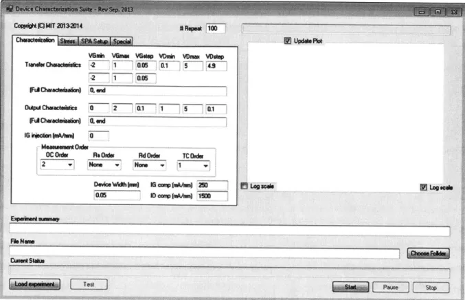
Figure 2-3. Characterization Interface written in C++ which enables alternative controls between the Accel-RF life test system and the external Keithley souce. ... 22
Figure 2-4. Experimental flow chart of the original high-power and high-temperature stress design... 24 Figure 2-5. (a) Phase 1, (b) Phase 11, flow chart of the improved experimental design... 26 Figure 3-1. High-power and high-temperature stress conditions for the original experimental approach (discussed in section 2.4) to study GaN HEMTs degradation. In this particular case, VDs is kept at 40V with
Tbase stepped up from 50 *C to 210 *C... 29
Figure 3-2. Stress conditions for (a) phase I of the improved experimental approach. In this particular case, VDs is kept at 40V with Tbas, stepped up from 50 *C to 220 *C. The entire 50 to 220 0C temperature ramp is repeated twice (b) phase 11 of the improved experimental approach. In this particular case, VDS is kept at 40V with Tbase stepped up from 120 0C to 215 *C. ... 30 Figure 3-3. (a) Comparison of drain current at the beginning of stress experiment and after higher-power DC stress at 220 0C. Both measurements are carried out after device is completely detrapped by baking at 250 0C for 7.5 hours. The degradation is permanent, absence of electron trapping. (b) Comparison of gate leakage current at the beginning of stress experiment and after high-power DC stress at 220 0C. Both measurements are carried out after device is completely detrapped. Threshold voltage has shifted in the negative direction and the ideality factor has degraded...31 Figure 3-4. Degradation of lDmax and I Gaff I of MMIC 25 Type B. The points sticking out in the graph are
measurements done following device detrapping (denoted as "outer loop data") and reflect permanent device degradation. The more clustered points are "inner loop data" which incorporate both electron trapping and permanent device degradation. Temperatures shown in the graph represent the stress tem perature Tbase which increases in steps ... 32
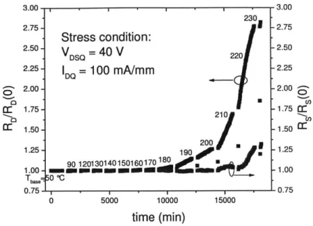
Figure 3-5. Degradation of RD and Rs of MMIC 25 Type B under high-power and high-temperature stress. After isolating electron trapping effects (as reflected by outer loop data), RD Still increases by about two
times. Rs, on the other hand, shows a much smaller increase...33 Figure 3-6. Degradation of lDmax and IIGo I of MMIC 29 Type B. The points sticking out in the graph are
Figure 3-7. Degradation of RD and Rs for MMIC 29 Type B under high-power and high-temperature stress. The overall degradation for both is negligible ... 34 Figure 3-8. Degradation of 'Dmax and
I
lGsf of MMIC 15 Type B. The points sticking out in the graph are measurements done following device detrapping and represent permanent device degradation. BothlDmax and iGff show little degradation... 34 Figure 3-9. Degradation of RD and Rs for MMIC 15 Type B under high-power and high-temperature stress. The overall degradation for both is negligible and Rs changes in the opposite direction as RD does...35 Figure 3-10. Degradation of lDmax and I lGoff I of MMIC 05 Type D. The points sticking out in the graph are
measurements done following device detrapping and represent permanent device degradation. Both IDmax and iGff show little degradation at Tbase = 50 0C. Significant drain current and gate leakage current
degradation emerges above Tbase = 190 0C ... 36 Figure 3-11. Degradation of RD and Rs of MMIC 05 Type D under high-power and high-temperature stress. RD starts to increase significantly from Tase = 190 0C and Rs shows no degradation... 36
Figure 3-13. IG vs. 'D degradation drawn with outer loop data. Only permanent device degradation is
reflected in the graph. ... 38 Figure 3-12. IG vS. ID degradation drawn with inner loop data. Both trapping related and permanent device degradation are included in the graph... 38 Figure 3-14. Degradation of 'Dmax and I Goff of MMIC 08 Type D during Phase I of the improved
experim ental approach...39 Figure 3-15. Degradation of 'Dmax and I lGf I of MMIC 08 Type D during Phase II of the improved experim ental approach...40 Figure 3-16. Degradation of IDmax and I lGoff lof MMIC 09 Type D during Phase I of the improved
experim ental approach...41 Figure 3-17. Degradation of IDmax and
IIGoff
I of MMIC 09 Type D during Phase II of the improvedexperim ental approach...42 Figure 3-18. Degradation of IDmax and I Go I of MMIC 11 Type D during Phase I of the improved
experim ental approach...43 Figure 3-19. Degradation of 'Dmax and IlGoff lof MMIC 11 Type D during Phase II of the improved experim ental approach...43 Figure 3-20. IG vs. 'D degradation drawn with (a) inner loop data where both trapping related and
permanent device degradation is included (b) outer loop data where only permanent device
degradation is reflected. Results of the four experiments under the original experimental approach as well as the three experiments under the improved approach are shown...44
Figure 3-21. Arrhenius plot of IDmax and RD for MMIC 25 Type B, where the points at each temperature Tj
is defined as the rate of change of variables during that specific temperature. (a) Ea extracted from the inner loop data reflecting both trap related and permanent degradation mechanisms (b) Ea extracted from the outer loop data reflecting only permanent device degradation...47 Figure 3-22. Arrhenius plot of IDmax and RD for MMIC 08 Type D (experiment conducted under the improved stress approach), where the points at each temperature T; is defined as the rate of change of variables during that specific temperature. (a) Ea extracted from the inner loop data reflecting both trap related and permanent degradation mechanisms (b) Ea extracted from the outer loop data reflecting only perm anent device degradation... 48
Figure 3-23. Arrhenius plot of 'Dmax and RD for MMIC 09 Type D (experiment conducted under the
improved stress approach), where the points at each temperature Tj is defined as the rate of change of variables during that specific temperature. (a) E8 extracted from the inner loop data reflecting both trap related and permanent degradation mechanisms (b) Ea extracted from the outer loop data reflecting only perm anent device degradation... 50 Figure 3-24. Arrhenius plot of lDmax and RD for MMIC 11 Type D (experiment conducted under the improved stress approach), where the points at each temperature Tj is defined as the rate of change of variables during that specific temperature. (a) Ea extracted from the inner loop data reflecting both trap related and permanent degradation mechanisms (b) Ea extracted from the outer loop data reflecting only perm anent device degradation... 50
Figure 4-1. SEM picture of the surface of MMIC 29 Type B. The overall permanent I Dmax degradation is
less than 1%. A shallow groove forms alone the gate edge on the drain side...54 Figure 4-2. SEM picture of the surface of device MMIC 05 Type D. The overall permanent IDmax
degradation is around 25%. Pits form at the gate edge on the drain side...54 Figure 4-3. SEM picture of the surface of device MMIC 05 Type D. Deep trenches form at the gate edge on the drain side at some locations along the gate width. ... 55 Figure 4-4. AFM picture of the surface of device MMIC 05 Type D. IDmax degradation for the device is around 25%. A Trench which is more than 20 nm in depth is clearly illustrated in the picture at the gate edge on the drain side. ... 55 Figure 4-5. (a) SEM picture at the center of gate finger of MMIC 29 Type B. IDmax degrades less than 1% for this device. A shallow groove forms alone the gate edge on the drain side. (b) SEM picture at one end of gate finger of MMIC 29 Type B. Similar to Fig. 4-5 (a), a shallow groove forms along the gate edge on the drain side ... . ..---.--.56 Figure 4-6 . SEM picture at (a) center of one of the two gate fingers (b) one end of one of the two gate fingers of device MMIC 15 Type B. IDmax degradation is about 5% for this device. Pits form at the gate edge and merge into trenches of some finite length at some locations...57 Figure 4-7. (a) SEM picture at the center of one of the two gate fingers of device MMIC 08 Type D. IDmax degradation is about 20% for this device. Pits form at the gate edge and merge into a continuous trench. (b) SEM picture at one end of one of the two gate fingers of device MMIC 08 Type D. Pits form at the gate edge and merge into almost continuous trenches... 58 Figure 4-8. (a) SEM picture at the center of one of the two gate fingers of device MMIC 09 Type D. lomax degradation is about 5% for this device. Pits form at the gate edge and merge into almost continuous trenches. (b) SEM picture at one end of one of the two gate fingers of device MMIC 09 Type D. High density pits form at the gate edge and merge into trenches at some locations...58 Figure 4-9. (a) SEM picture at the center of one of the two gate fingers of device MMIC 05 Type D. I Dmax
degradation is about 25% for this device.Pits form at the gate edge and merge into a continuous trench. (b) SEM picture at the center of one of the two gate fingers of device MMIC 05 Type D. Pits form at the gate edge and merge into almost continuous trenches... 59
Figure 4-11. A 1 x 1 pm AFM scan of device MMIC 15 Type B at the center of one of the two gate fingers. lDmax degradation is about 5% for this device. Pits form at the gate edge on the drain side...60 Figure 4-12. A 1 x 1 pam AFM scan of device MMIC 08 Type D at the center of one of the two gate fingers. lDmax degradation is about 20% for this device. Pits with high density form at the gate edge on the drain side and merge into an almost continuous trench along the gate width... 61 Figure 4-13. A 1 x 1 pm AFM scan of device MMIC 09 Type D at the center of one of the two gate fingers.
IDmax degradation is about 5% for this device. Pits with high density form at the gate edge on the drain side and merge into an almost continuous trench along the gate width. The depths of the pits are not as large as those in Fig. 4-12. ... 62 Figure 4-14. A 1 x 1 pm AFM scan of device MMIC 05 Type D at the center of one of the two gate fingers. X-axis represents the direction along gate length and y-axis represents the direction along gate width. A continuous trench forms at the gate edge throughout the 1 pm scan in y-axis direction...63 Figure 4-15. Cross-sectional view of a delaminated device showing the trench formed at the gate edge on the drain side as well as the gate undercut. "Trench width", "Pit depth", and "Erosion depth" are defined as shown in the figure. All quantities are averaged across a 1 pm scan in the gate width direction.
... 6 3 Figure 4-16. Distribution of pit depth along half of the gate width for the device with an overall I Dmax
degradation of 21.6%. Each point in the graph represents an averaged value across a 5 pam scan... 66 Figure 5-1. Correlation between electrical and structural degradation of the five devices biased under high-power stress regime. Both 'Dmax degradation vs. Trench width and IDmax degradation vs. Pit depth are
shown. (a) IDmax degradation i calculated from inner loop data (b) 'Dmax degradation is calculated from
outer loop data...70 Figure 5-2. Correlation between the overall channel resistance RCH degradation and the erosion in the gate regio n...7 1
List of Tables
Table 1-2. Summary of long-term accelerated tests on GaN HEMTs carried out by industrial laboratories. [26]... ... ... -...16 Table 2-1. Definition of device parameters measured. ... 23
Table 4-1. For each of the five devices, gate fingers have been indexed with number 1 and 2. In both fingers of all five devices, the distance from the gate edge to the edge of the drain contact is measured under SEM. In every case, the gate finger that is closer to the drain contact has more severe structural dam age. ...- ... . ---... 65 Table 5-1. Overall drain current degradation of the five devices discussed in Chapter 4. Outer loop data are measurements after complete device detrapping which means that only permanent degradation is reflected in the data. Inner loop data, on the other hand, are measurements conducted without
Chapter 1. Introduction
The idea of the HEMT (high electron mobility transistor) structure was first brought out by Takashi
Mimura in 1979 [1]. During the following year, both depletion-mode [2]and enhancement-mode [3]HEMTs on an AIGaAs/GaAs heterostructure were demonstrated. Conventional MOSFET structures
rely on high electron or hole densities introduced by n- or p- type dopants to conduct current. The
introduction of dopants in semiconductor material, while guaranteeing high carrier densities, also limits the mobility of these free carriers due to scattering with impurities. HEMTs avoid this by utilizing
heterojunction of a highly-doped wide-bandgap n-type donor-supply layer and a non-doped channel layer without introducing impurities in the channel itself. This results in the extremely high electron
mobility and makes the HEMT structure promising for electronic applications.
1.1 Introduction to GaN HEMTs
Ever since the first demonstration of high electron mobility transistor based on a GaN/AlxGa1-xN
heterojunction in 1993 by Khan et. al [5], its development has skyrocketed. Due to its high electron mobility, high breakdown field, and high power density, GaN is a promising candidate for high power and high frequency applications. Compared with GaAs which has a basic power density of about 1.5
W/mm, GaN is able to reach a power density as high as 12 W/mm. This gives GaN based power amplifiers a huge advantage in that for the same power level, multiple GaAs based devices will be necessary while a single GaN based device is enough.
As illustrated in Fig. 1-1, the key characteristics of GaN, i. e. high dielectric strength, high operating
temperature, high current density, high speed switching and low on-resistance make it an extremely promising material for power electronics applications. Table 1-1 summarizes some of the main material
properties of GaN compared with other semiconductors used for power devices applications. The
simultaneously achievable high breakdown field, high operation temperature, and large bandgap make GaN superior to other semiconductors.
Advantageous power supply c High breekdown Due to large bandgap Advantag Power SUP High maxim Due to I* density a eleewonr
Advantageous In power supply circuits High operating temperature
Due to large bandgap and high potential barrier
(RwC)
in Advantageous in
ircuitsl 300, a RIF circuits
strength G0N High maximum
oscillation frequency Due to high electric field eaturatlon speed
N4rn) (GHz) and low parasitic
capacity
Si
GAs
apus in Gas Advantageous In
ply circuits RIF circuits
urn current Superior noise factor
;h carrier
.
Due to low carrier calterinond high yihlm)
nobility
(dB) and low RF losses
Figure 1-1. Key advantages of GaN compared with that of GaAs and Si. [4]
Material Mobility Dielectric Bandgap, Breakdown field Tm.,
p, cm2/V.s
Constant Eg, eV Eb, 106 V/cm 0C
E
Si 1300 11.9 1.12 0.3 300
GaAs 5000 12.5 1.42 0.4 300
4H-SiC 260 10 3.2 3.5 600
GaN 1500 9.5 3.4 2 700
Table 1-1. Material Properties of Microwave Semiconductors [6].
1.2 Previous Studies on Reliability
Despite the excellent performance and rapid development of AIGaN/GaN HEMTs, reliability is a serious issue without solving which the wide deployment of GaN based transistors will be impossible. Considerable research has been conducted in trying to figure out the underlying physics of various device degradation mechanisms. Up to now, the demonstrated degradation mechanisms include but are not limited to:
1) Inverse piezoelectric effect 2) Time-dependent trap formation
3) Percolative conductive paths formation 4) Electrochemical AIGaN and GaN degradation
Ever since the first observation by Joh and del Alamo [7], the degradation mode of GaN HEMTs under reverse gate bias consisting in an increase of gate leakage current and an enhancement of current
collapse has been repeatedly observed by many other authors [8]-[19][20]. The mechanism involves defects existing at the gate edges which can promote the injection of electrons from the gate contact
into the AIGaN barrier layer through a trap-assisted tunneling mechanism [10]. Those defects can be
introduced during growth of the AIGaN/GaN heterostructure or during stress with gate being reverse biased which imposes a very high electric field at the gate edges. An electrical signature of such
degradation mode is the presence of a critical voltage Vcr of |VG| above which a sudden gate leakage current increase of several orders of magnitude is observed. The physical explanation of such
degradation mechanism takes into consideration the piezoelectric nature of GaN and AIGaN materials as well as the extremely high vertical electric field within the AIGaN barrier layer in a HEMT. When reverse bias is applied, the vertical component of the electric field at the gate-drain edge increases sharply. This
in turn enhances the tensile strain and the stored elastic energy brought about by the inverse
piezoelectric effect. The enhancement is most severe at the gate edge where the electric field reaches its maximum value. Once a certain critical level of stored energy or strain is reached, crystallographic
defects can be produced in the AIGaN layer. These defects will then degrade the electrical characteristics of the transistor by affecting transport properties or by inducing trapping effect.
Biasing GaN HEMTs below Vent itself, however, cannot guarantee the avoidance of device failure. As demonstrated by Marcon et al. [21] and Meneghini [22], if devices are stressed at constant reverse gate voltage for a sufficiently long time, catastrophic gate leakage increase may occur even below the critical
voltage. Fig. 1-2 demonstrates such a situation where device is stressed under VG = -30 V (Vcrt= -35 V). Sudden increase of gate leakage happens after a sufficiently long stress time. To explain this, Meneghini
et al. has proposed a percolative model where for long stress times, defects may be randomly generated within the AIGaN layer, due to the inverse piezoelectric effect or to the high electric field, which can lead
tU32
So
t2000
6
-4.o
3
5
Constant Voltage
Stress
.0-3.0
=30V,.,IV-2-.5
-2.0
(a8)
10
100
10003600
Stress
Time
(s)
1000
-95
-
-
-
-1
CNoise increases>500
before damage -2.000~
-2.05
E
(b)>()
_0 (C)Z 100
2.1
L 100ioo
10 100 1000 10 1000Stress time (s)
Stress Time
(s)
Figure 1-2. Results of a constant-voltage reverse-bias stress test. The three graphs report the variation of (a) gate current, (b) amplitude of the noise on gate current, and (c) threshold voltage during stress time. Vt for the specific device is around -35 V [22].
Besides degradation of the Schottky gate, another reliability concern in GaN HEMTs is related to the
degradation of drain saturation current and the overall output power. In [23], a direct correlation between the saturation drain current and structural degradation at the gate edge of GaN HEMTs
stressed under OFF-state regime is established as illustrated in Fig. 1-3. Gao et al. [24] proposed an explanation for the structural degradation in AIGaN/GaN HEMTs under OFF-state stress where they
postulate that water from the passivation layer surface and the external atmosphere, as well as holes caused by trap-assisted interband tunneling in the AIGaN barrier are likely to play an essential role in
forming the surface pits. Moreover, they proposed that permanent drain current degradation is due to
the reduction of the AIGaN barrier caused by surface pitting. However, a more detailed and
(a)
U
I:0
&
02 4 &8
Depth of defectiveregl on(nm)
(b)
2
46
#1 [2.20
Depth of deetilVel"egon (war)
Figure 1-3. Correlation between electrical and structural degradation for AIGaN/GaN HEMVTs degraded under OFF-state conditions: (a) permanent 6n.a degradation vs. pit depth and (b) current collapse after stress vs. pit depth [23].
1.3 Motivation
The reliability of GaN HEMTs has greatly improved in recent years. The improvements include but are not limited to: suppression of current collapse to a large extent by passivating surface states using
deposited or in-situ grown SiN , increase of DC breakdown voltage by utilizing field plates [25], and reduction of problems related with gate leakage current and its stability by engineering of the gate
electrode, contact and recess area. Another important issue in a device technology is the value of mean
time to failure (MTTF). The usually extremely long values are commonly derived by extrapolating the results of three-temperatures DC or RF accelerated tests according to the Arrhenius law and by using a
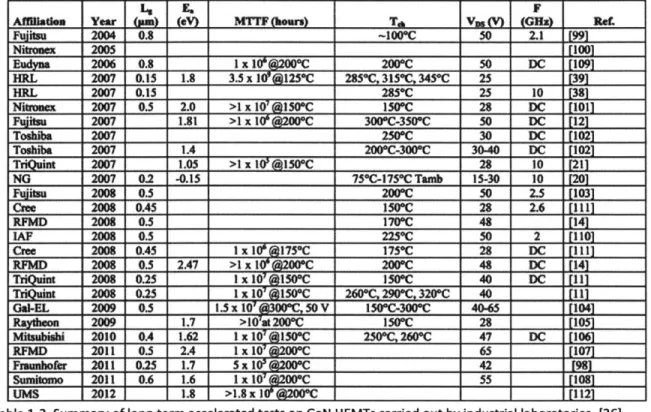
groups involved [26]. From the table, we can see that there is a large range of MTTF extracted by different laboratories on different technologies. It is not very meaningful for us to compare these values. To achieve more meaningful comparisons, there are still some problems left to be solved. First of all, the extrapolation of an MTTF requires knowing the activation energy with absolute certainty which is not
always declared by the laboratories. Secondly, the activation energy is usually derived using high temperature testing. It is possible that high Ea mechanisms dominate at high temperatures while low Ea mechanisms dominate at lower temperatures which are relevant in actual device operation. By carrying out high temperature tests only, the low activation energy mechanisms might be overlooked. Thirdly,
the interaction of the different accelerating factors (in particular current, temperature and voltage or
electric field) is not known.
4 Fe F
ANfhatIm Year pa) ) MTF (horn) TA Vu (G3N) PAL
Fjitsu
2004 0.8 -100*C 50 2.1 WNitroex
2005 [1___ Eudym 2006 0.8 1 x le#22C 200C 50 DC [1091 HIL 2007 0.15 1.8 3.5 x I0@125*C 285'C.315*C.34*C 25 [391 HRL 2007 0.15 285*C 25 10 [M Niuata 2007 0.5 2.0 >1 xKo1MC
1509C 28 DC [101]Fuitpu 2007 1.81 >1 x I200C 30DOC-350VC 50 DC [121
Toshiba 2007 2S0C 30 DC no2f Toshiba 2007 1.4 200*C-300"C 30.40 DC [102] T . 2007 1.05 >1 x10'l150*C 28
10
[211 NG 2007 0.2 -0.15 750C-1730C Tamb 15-30 10 L201 bditsH 2008 0.5 2000C 50 2.5 LPJ Cre 2008 OAS _150C 28 2.6 [111 RFMD 2008 0.5 170C 48 14 IAP 2008 0.5 22WOC 50 2 [1101 Cme 2008 0.45 1 x WNIV5C 1759C 28 DC [111] RFMD 2008 0.5 2.47 >1 X IW@2w0C 200C 48 DC [141 TrW . 2008 0.25 1 X I415M 150C 40 DC [111TrOWIn 2008 0.25 I X14 IVhi *C 260C.290C. 320*C 40 fill
Gal-EL 2009 0.5 .5 X 1WJOEM, 50 V l50'C-300C 4065 [1041 Ray*ew 2009 1.7 >10'at 200C 1500C 28 [1051 Mtsubishi 2010 0A 1.62 1 X
I
W 250"C 2600C 47 DC [1061 RFMD 2011 0.5 2.4 1 00 C ___#RPM65 [_10 Fzuumofer 20110.25
1.7
5 a I 010A@2C 42 9_1 Sumitomo 2011 0.6 1.6 1 x IW 00PC 55 [108] UMS 20121.8
>1.8x1 @200*C 11121Table 1-2. Summary of long-term accelerated tests on GaN HEMTs carried out by industrial laboratories. [26]. Considering all the above described improvements and problems still left to be solved, one goal of this project is to develop a stress methodology which can reveal the activation energy of device degradation
rate from measurements on a single device. The underlying idea is to utilize step temperature stress
where degradation rates at a wide range of stress temperatures are measured so that the ultimate Ea value obtained reflects both low temperature degradation mechanisms and high temperature degradation mechanisms. Besides this, we will also study the various degradation mechanisms of GaN
HEMTs stressed under high-power regime, which, despite its importance in RF applications, has received little attention compared with OFF-state stress regime. Thirdly, we will establish a quantitative
correlation between electrical degradation and structural degradation.
1.4 Thesis Outline
The thesis is organized in the following way:
In Chapter 2, we will first introduce the devices studied in this thesis as well as the experimental
techniques that have been utilized. Following that, we will describe our designed characterization suite. Both electrical stress methodology and surface examination procedures will also be introduced.
In Chapter 3, the results of electrical degradation of selected experiments will be shown where we have
identified two sequential degradation mechanisms with different electrical signatures. Activation energies of degradation rates are extracted and compared with values obtained from conventional
method on a similar device technology.
In Chapter 4, the results of structure degradation of the same selected experiments as in Chapter 3 will
be shown where we have formed a hypothesis of two stages in structural degradation corresponding to the two mechanisms revealed in Chapter 3.
In Chapter 5, quantitative analysis of the correlations between electrical and structural degradation will be investigated.
Chapter 2. Experimental
2.1 Introduction
This chapter describes the devices, instrumentation setup, as well as the stress methodology adopted in
this thesis. It begins with a description of the GaN HEMTs that are used for this study. Then the experimental setup and characterization suite developed for evaluating the various figures of merit will
be discussed. Finally the tools and characterization approach used in device surface examination will be explained.
2.2 Devices
Figure 2-1 shows a schematic cross section of the GaN HEMT used in this study. These devices are fabricated by TriQuint Seminconductor. The device has Fe-doped GaN buffer deposited on a SiC
substrate. Then a 16 nm AlGaN barrier layer with 28% Al mole fraction is used. 2DEG (2-D Electron Gas) is formed at the intersection of the AIGaN barrier layer and the GaN buffer due to spontaneous
polarization of the AlGaN barrier as well as the strain introduced by lattice mismatch between the two materials. On top of the barrier layer is a 5-nm GaN cap layer.
All the devices investigated in this study have a 0.25 im gate length and a 2 x 260 Ipm gate width. The geometry of the gate is a standard S-Band design with 2 prm gate-source spacing and 4 pm gate-drain
spacing.
The actual samples available for testing are individual GaN power amplifiers in MMIC (Monolithic
Microwave Integrated Circuit) form. A device thermal model has been provided by TriQuint Semiconductor for estimation of transistor junction temperatures.
Figure 2-1. Schematic two-dimensional cross section of GaN HEMT (graph is not drawn to scale).
2.3 Electrical Experiments
The stress condition that is the focus of this study is the DC high-power and high-temperature stress regime. Devices are stressed under various VDs and IDQ high power conditions with base plate
temperature raised from some starting temperature (higher than room temperature) in steps until the device finally blows up. Since the devices are in MMIC forms, a probe station is not suitable for device stressing and characterization. Instead, all our experiments are carried out on a four-channel Accel-RF life test system. Due to the unique properties of GaN HEMTs, electron trapping needs to be taken into consideration in order to distinguish it from permanent device degradation. We have developed a detrapping technique based on a thermal treatment of the devices. A benign characterization suite is adopted from [27] to characterize the device figures of merit before, during, and after stress experiments.
Figure 2-2. System configuration of stress test and characterization setup. Adopted from [28].
2.3.1 Experimental Setup
The experimental instruments used for this project are shown in Fig. 2-2. An Accel-RF AARTS
RF10000-4/S system and a Keithley 2400 DC Source are used for device stress and characterization. The Accel-RF system has four channels, capable of stressing four devices simultaneously. The main components of the Accel-RF are Power Control Unit, Heater Control Unit, and RF Control Unit. In this project, the Power Control Unit is utilized to apply DC high power stress to the device under test (DUT) and the Heater
Control Unit is utilized to apply step temperature stress to the DUT. The system is controlled by a windows-based PC. An internal switching matrix controls to which channel the stress is applied. For our
study, an external Keithley 2400 DC source is connected to the Accel-RF system to carry out device characterization. Execution of the Accel-RF system and the external Keithley source are alternated with token files passed between the two. A C++ interface has been developed by J. Joh [27] and is utilized for this project to enable passing of token files to be incorporated into long routines which can run
automatically. As shown in Fig. 2-3, this C++ interface enables users to design new experiments easily without changing the structure of the whole program.
#iRWp"t 100 ComwlOOuircsiudo4 V5mh VOma. VGp Vomin Vnm VWs p 2 1 OS pJRAchafiuhakn) G..u esAchaa& 2 01 1 5 0.1 (ichwactsudalin) 0.md M ...m...u
OCOni. Phoi. RdO. TC...
2 None Non 1
d0 ID comp WwO IWO
J~g.
FisNawb
Figure 2-3. Characterization Interface written in C++ which enables alternative controls between the Accel-RF life test system and the external Keithley souce.
2.3.2 Characterization Suite
Since we anticipate the characterization of devices to be repeated many times for our study of device degradation under various stresses, it is important to develop a characterization suite that can accurately reflect device electrical performances even with certain level of degradation. At the same time, the characterization suite must be benign enough such that repeated characterization itself will not significantly degrade the devices. Under this philosophy and after testing, we have adopted a characterization suite that is similar to that in [27].
I
Parameter Definition
IDmax Drain current at VDS = 5 V and VGs = 2 V
Rs Source resistance measured with IG = 20 mA/mm
RD Drain resistance measured with IG = 20 mA/mm
RTOT Total resistance between drain and source with gate floating
RCH Channel resistance. RTOT - Rs - RD
VT VGS- 0.5VDS when ID =
1mA/mm
at VDS = 0.1 VSS Sub-threshold slope at VDS = 0.1 V and ID = 1 mA/mm
DIBL VTIVDSo=.1v- VTIvDs=sv
gmpk Peak transconductance dID/dVGs at VDS = 5 V
lGoff Gate current at VGS = 5 V and VDS = 0.1 V
Table 2-1. Definition of device parameters measured.
Table 2-1 shows the definition of various figures of merit to be monitored for our devices. Here, Rs and
RD are measured using the gate current injection technique as described in [29]. In these measurements,
the drain or source current are forced to 0 while current is injected into gate. The voltage drop across
gate-source or gate-drain, allows Rs or RD to be extracted respectively.
2.3.3 Device Detrapping
Due to imperfect epilayer growth and some of the unique properties of the AIGaN/GaN heterostructure
such as spontaneous polarization and lattice mismatch, both reversible and permanent device degradation take place in GaN HEMTs under stress, as have been demonstrated by several authors
[30]-[32]. The reversible device degradation is believed to be caused by surface or bulk defects which can trap electrons and thus alter conduction band discontinuity as well as Schottky barrier height. Some of the typical manifestations of electron trapping in device electrical performance are a decrease in drain
current and gate leakage current, an increase in resistance, as well as a negative shift of the threshold voltage. However, these changes are not permanent and do not reflect any structural degradation of the
devices. We have sought to develop a technique to detrap those electrons and thus be able to isolate
permanent device degradation. Usually, exposure to UV light (of an energy that might depend on device types due to the different energy levels of traps) turns out to be an effective and fast way to detrap electrons. However, since our DUTs are packaged, we have instead adopted a thermal treatment
method. Based on repeated tests, we have found that baking at 250 *C for 7.5 hours can completely eliminate electron trapping in our devices.
2.4 Stress Test Methodology
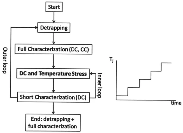
Our stress tests are designed to study device degradation under high-power and high-temperature stress. The DC bias is fixed at a certain level with base plate temperature stepped up to study the dependence of degradation on temperature. To be able to monitor the evolution of various device figures of merit under stress, we would need to pause stress periodically and carry out characterization. Taking into account the fact that prolonged stress would introduce significant electron trapping, we would also need to detrap the devices occasionally in order to distinguish reversible trapping effect from permanent device degradation. Incorporating all these, the flow chart of our original design is shown in Fig. 2-4.
Start
Detrapping
o
Full Characterization (DC, CC)
0 *0DC and Temperature
Stress
-
Short Characterization (DC)
End: detrapping+
full characterization
Figure 2-4. Experimental flow chart of the original high-power and high-temperature stress design.
Due to the fact that even a virgin GaN HEMT contains a significant amount of defects capable of trapping electrons, the very first step in our experiments is to bake the device at 250 *C for 7.5 hours in order to fully detrap all electrons. After the device is initialized in this way to a "clean" state, i. e., without any trapped electrons, a full characterization is conducted at Task, = 50 C where various figures of merit are extracted such as 'Dma, VT, gmpk, Goff, RD, Rs, etc. Following this, we start to apply stress with a fixed VDs
and IDQ bias at a certain starting base plate temperature which is chosen to be 50 *C. The stress would
last for 20 minutes after which we pause the stress, conduct a short characterization of selected figures
of merit at base plate temperature of 50 0C. This stress and short characterization together compose the
"inner loop" of the experiment. The entire inner loop repeats 20 times before we stop the stress again, conduct a detrapping step followed by complete I-V sweep characterization. The device is then stressed
under the "inner loop" regime again at a higher base plate temperature. The detrapping, full
characterization, and "inner loop" together compose the "outer loop". The entire experiment continues with base plate temperature raised up in steps until the device finally blows up.
An improved experimental approach was also developed. After several experiments carried out under
the original approach, we found that gate leakage current turns out to degrade rather fast and the degradation saturates above some base plate temperature. The drain current, on the other hand,
degrades rather slowly and only after the gate leakage degradation has saturated. This leads us to develop a procedure in which we first degrade the gate current without significant drain current degradation. After gate current degradation has saturated, we then focus on the degradation of drain
current. Thus, a two-phase experimental approach is proposed as shown in Fig. 2-5.
In phase I, the big idea is to apply very short high-power step-temperature stress to achieve fast gate leakage current degradation without prominent degradation in drain current. As shown in Fig. 2-5 (a), in
this approach, the experiment starts with an initial detrapping step followed by full device characterization. Then we move onto applying stress at fixed VDS and IDQ at a starting base plate
temperature of 50 *C. The stress lasts for 3 minutes after which we pause the stress, characterize the device at 50 0C and stress the device under the same condition for another 3 minutes. Following this, the base plate temperature is raised by 20 *C and the process is repeated. We follow the same procedure at each base plate temperature from 50 0C to 220 *C in 20 *C step. After the 220 *C stress, the entire procedure is repeated a second time to make sure that gate leakage current degradation is well
saturated. The reason we stop at 220 *C is based on our previous experience such that base plate temperature exceeding 220 *C might lead to ultimate failure of the device.
After phase I, we check to see if gate leakage current has indeed saturated before we move on to phase
11. Then different from phase I, the stress period during phase I at each base plate temperature is much longer. As shown in Fig. 2-5 (b), we again start the experiment by a complete detrapping at 250 *C for
conduct a device characterization at 50 *C. This is repeated 8 times. After the eight one-hour stress periods, we carry out a short detrapping step at 250 "C for 1.5 hours. Instead of the 7.5-hour long detrapping, here for the sake of conserving time, we only bake the device for 1.5 hours. This turns out to
partially but not completely detrap the device as we will show in Chapter 3. Then the sequence of eight one-hour stress followed by a short detrapping step is repeated 3 times at the same stress level. That is
to say, the device is stressed for a total time of 24 hours at each base plate temperature level. This
process continues with the base plate temperature increased in steps until finally the device blows up.
(a)
Start
Detrapping
y
DC Characterization
DC Stress
(at Ts. for 3 minutes)
DC Characterization
k
-I3
0 00 -I g II -1 + N 0S(b)
Start
Long Detrapping
Characterization (DC)
DC and Temperature Stress
Short Detrapping
Characterization (DC)
End: detrapping+
full characterization
Figure 2-5. (a) Phase 1, (b) Phase 11, flow chart of the improved experimental design.
2.5 Device Delamination and Surface Examination
An important component of this study involves the examination of the surface of stressed devices in an attempt to correlate electrical degradation with structural degradation. A Zeiss Supra 40 SEM and an
AFM-Nanoscope IV Scanned Probe Microscope have been used in device surface analysis. To be able to
DC Stress
(at Tw. for 3 minutes)
observe the actual semiconductor surface, before SEM or AFM scanning, we have conducted a three-step process to remove the metal contacts for source, gate, and drain, as well as the SiN passivation
layer [33].
2.5.1 Process and Machines
Similar to [33], SiN is first etched away in HF : H20 (1:10) solution for 10 minutes following which metal
contacts are removed in aqua regia, i. e., HCI : HNO3 (3:1) under 80 "C for 40 minutes. The last step is the cleaning in H2SO4 : H202 (3:1) for 10 minutes. After this three-step wet etching process is completed, the
device is ready for surface examination. The high resolution down to several nanometers of the Zeiss
Supra-40 SEM makes it possible for us to scrutinize the device surface efficiently even if the features we would like to observe are on the nanometer scale. The AFM-Nanoscope IV Scanned Probe Microscope,
on the other hand, enables quantitative analysis of the features of interest. Both the Zeiss Supra-40 SEM and the AFM-Nanoscope IV Scanned Probe Microscope have Windows-based control software which
enables easy operation and data analysis.
2.5.2 Characterization Approach
In our surface characterization approach, we first obtain scans of the entire GaN HEMT on the chip using
SEM. We follow this with a detailed SEM examination at the device gate edge on both the source side and drain side across the entire gate finger width. Since our devices have two gate fingers, this process needs to be repeated twice. For our devices stressed under high-power and high-temperature, it has
been found that between the two gate fingers, there is always one finger that has more severe structural damage than the other finger. Also, it has been noticed that the center of each gate finger is
more vulnerable to physical damage than the two ends of the gate finger.
AFM has higher spatial resolution but is very limited in scope. Because of this, we have focused our AFM
analysis on the central region of the gate finger with more physical damage. We conduct multiple 1 x 1
prm scans around the center of gate fingers as representatives of the physical degradation of the device. Data carried by those scans are analyzed and averaged for each device.
2.6 Summary
In this chapter, we have introduced the devices studied in this thesis as well as the experimental techniques that have been utilized. A benign characterization suite is adopted based on the study in [27]. We have gone through the techniques and methodology employed, which are SEM and AFM scans, in analyzing surfaces of stressed devices. We have come out with two experimental designs for step-temperature stress experiments with the device biased in the high-power state. In the next chapter, results of electrical degradation will be shown and the degradation phenomena will be discussed.
Chapter 3. Electrical Degradation
In the previous chapter, we have discussed basic experimental approaches to study the electrical and structural degradation of GaN HEMTs. Now, in this chapter, we will be diving into the detailed results of device electrical degradation experiments and the mechanisms lying behind the observed phenomena.
3.1 Overall Degradation Phenomena
As described in chapter 2, shown in Fig. 3-1 is a typical experiment profile for a power and high-temperature stress experiment in our original experimental approach. VDs is maintained at a certain level (40 V or 50 V depending on specific experiment). In or der to maintain IDQ at a relatively constant
value around 100 mA/mm, frequently measured values of the actually 'D under the stress voltage is used
as a feedback to the Power control unit. If there is any lD deviation from the target value due to device degradation, this feedback will enable the Power control unit to adjust the applied gate bias VGS accordingly in order to bring 'D back to 100 mA/mm. The base plate temperature, Tbase, is raised in step
from 50 0 C to above 200 0
C until the device blows up.
50 . 1 , . ,,I 24 0 U) U) 0 U) U, 0 40-30 - 20- 10-0m
0
5000 10000time (min)
15000 -220 -200 180 160 140 120 100 80 60 , 40 0000 0 U in1Im~i --2Fig. 3-2 (a) shows the typical stress conditions for phase I of the improved approach (discussed in section 2.4). In this case, VDs and lQ are maintained at 40 V and 100 mA/mm with Tbase raised from 50 *C to 220 *C in 20 *C steps. The ramping from 50 to 220 *C is repeated several times to make sure that gate leakage current degradation has been driven into saturation. The total stress time at each temperature is kept short at 6 minutes to ensure that no significant drain current degradation happens. Fig. 3-2 (b) shows the stress condition for phase 11 of the improved approach. Again, VDs and IDQ are maintained at 40 V and 100 mA/mm. Tbase, however, is raised from 120 *C to 215 *C and the total stress time at each
temperature, that is 24 hours or 36 hours depending on specific experiment, is much longer than that in phase 1, in order to sufficiently degrade drain current.
(!) 50 ' ' ' ' ' ' Cl, 03 U . -221 40- 201 40 - m mO.. . E E S =Eu.eee -18 U U 30 -16(1 -141 20 12 -10( 10- -80 U U 60 0. An -220 40.- o eim -0---- 200 30-> 180-20- -160 140 10--120 0 . 0 500 100 1500 2000 2500 3000 0 2000 4000 60 80 10000 120001400 16000
time (min) time (min)
Figure 3-2. Stress conditions for (a) phase I of the improved experimental approach. In this particular case, VDS is
kept at 40V with T.,. stepped up from 50 *C to 220 *C. The entire 50 to 220 *C temperature ramp is repeated twice (b) phase
11
of the improved experimental approach. In this particular case, VDS is kept at 40V with Tb.. stepped upfrom 120 *C to 215 *C.
Fig. 3-3 (a) and (b) show the changes in drain current ID and gate current IG before and after the application of high-power high-temperature stress for a typical device. This is the result of the combined effects of Phase I and Phase 11 such that both gate leakage current and the maximum drain current are degraded. From the graph, we see that 'D has decreased by 67% at VDS = 5 V from around 750 mA/mm down to 250 mA/mm. Since the two measurements are carried out after complete detrapping, the change in ID is due to permanent degradation. From Fig. 3-3 (b), we can notice that the overall gate
leakage current has increased by about 2 orders of magnitude. Threshold voltage has shifted in the negative direction (not shown) and the ideality factor has also degraded indicating damage of the Schottky contact.
* After initial detrapping
* After detrappina following stress at 220 OC
VGS 2 V U 0 1 2 3 4 5 V0s (V) (b) 10. 11 0.1 E E 00 - 1E-3, 1E-4 1E-5
m After initial detrapping
* After detrapping following stress at 220 C
VDS =0.1 V ""r "" * * 800 700- 600-500 400- 300- 200- 100-0 0
Figure 3-3. (a) Comparison of drain current at the beginning of stress experiment and after higher-power DC stress at 220 0
C. Both measurements are carried out after device is completely detrapped by baking at 250 *C for 7.5 hours. The degradation is permanent, absence of electron trapping. (b) Comparison of gate leakage current at the beginning of stress experiment and after high-power DC stress at 220 'C. Both measurements are carried out after device is completely detrapped. Threshold voltage has shifted in the negative direction and the ideality factor has degraded.
3.2 Original Approach
In Chapter 2, we have introduced the stress methodology of our original approach where a device is stressed at a fixed DC level with the base plate temperature stepping up. Under such stress, device degradation happens as manifested through various figures of merit such as 'Dmax, 'Goff, VT, RD, etc. Shown in Fig. 3-4 are the changes in normalized IDma, and 'Goff as the base plate temperature is ramped up for a
device labeled MMIC 25 Type B. We can notice from the right graph that below 170 *C, 'Goff stays at a
relatively constant level. However, starting from 170 *C, 'Goff increases dramatically by about three
orders of magnitude until Tase reaches 190 *C, after which the change in 'Goff saturates. Correspondingly,
from the left graph, we notice that below 180 *C, IDmax, shows very small degradation which is mainly due
to electron trapping. However, starting from 190 0C, significant drain current degradation emerges and by the end of 220 *C stress, the permanent degradation of lamax, is as high as 67%. Also, by qualitatively comparing the decrease of 'Omax at each base plate temperature level, we can observe that at higher
temperatures, 'Dmax decreases more. This indicates a thermally activated behavior of IDmax, degradation.
(a)
E E E -6 -4 -2 VGS (i 2outer loop data, which are represented by points sticking out, show thermally activated degradation trend. Rs, on the other hand, has a much smaller increase compared with RD. This is different from what have been reported under VDS = 0 V stress where RD and Rs change in similar ways [10], [11], [23]. However, the result is similar to ON-state experiment reported in [34]. This indicates that the high electric field on the gate edge at drain side might be a significant driving factor for RD degradation.
90120130 150 170 outer loop data
=50 'C 140 160 180 . 190 200 E E , 210 Stress condition: VDSQ =40 V 22 lO = 100 mA/mm 230 0 4000 8000 12000 16000 time (min) 0.1 0.01 1 E-3
outer loop data -- , 0210 220
10 2001 220 . 1 8 02 3 120 130 1 s0 0 140150 S170 W 0 4000 8000 12000 16000 time (min)
Figure 3-4. Degradation of IDax and I offI of MMIC 25 Type B. The points sticking out in the graph are
measurements done following device detrapping (denoted as "outer loop data") and reflect permanent device degradation. The more clustered points are "inner loop data" which incorporate both electron trapping and permanent device degradation. Temperatures shown in the graph represent the stress temperature Tsa. which increases in steps.
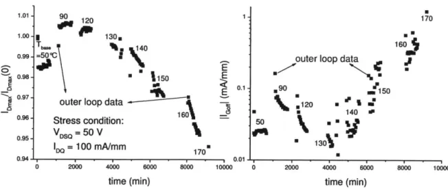
Besides this experiment, we have carried out same type of high-power high-temperature experiments on more devices. Shown in Fig. 3-6 is the degradation of MMIC 29 Type B. Base plate temperature is raise from 50 C directly to 190 *C to conserve time since we believe that higher temperature may be able to accelerate the device degradation so that a higher degree of degradation may be induced. From the right graph, we can see that the initial gate leakage current is rather large and the overall lGaff
degradation is small compared with MMIC 25 Type B. By the end of the experiment, I G I is still
increasing and has not saturated yet. At the same time, as shown in the left graph, the drain current experiences very small degradation and most of it is due to electron trapping. Fig. 3-7 shows the drain and source resistance degradation of the same device. Consistent with 'Dmax degradation, both RD and Rs
show negligible degradation.
1.0- 0.8- 0.6- 0.4- 0.2-E E __
Stress condition:
VDSQ40
V
IDO
=100 mA/mm
* T 2301 220 2.75- 2.50- 2.25- 2.00-1.75 -1.50 -1.25 -1.00 -T 0a 0.75-0 5000 10000time (min)
-3.00 -2.75 -2.50 -2.25 -2.00 -1.75 -1.50 -1.25 -1.00 0.75 15000Figure 3-5. Degradation of RD and Rs of MMIC 25 Type B under high-power and high-temperature stress. After isolating electron trapping effects (as reflected by outer loop data), RD still increases by about two times. Rs, on the other hand, shows a much smaller increase.
0 T =c o-C .% outer lo E190 * .U 200 205 Stress condition: VDSQ = 40 V lO = 100
mA/mm
0 2000 40 time (min) op data E UE E 210 " " V 215 220 0.4- 0.2- 0.0-6000 8000 0outer loop data
210 m215 220 I .U 205
M
50 " 190 0 200 ,Iftalo:
2000 4000 time (min) 6000 8000Figure 3-6. Degradation of lma and IIGo of MMIC 29 Type B. The points sticking out in the graph are
measurements done following device detrapping and represent permanent device degradation. Both I m,, and lIoff
show little degradation.
Another similar stress experiment is carried out on MMIC 15 Type B as shown in Fig. 3-8. Below Tbase =
120 *C, the drain current shows little increase during each temperature stress cycle. Similarly, the gate leakage current
IGoff
I decreases during each temperature stress cycle. These are signs of incompleteS.
0a:
0 210 20070
90 120130140150160170180 190 50 "C C, CI)cc
_ 1.015- 1.010- 1.005- 1.000- 0.995-0.990.our detrapping technique does not work as well on this device as on others. At higher stress temperatures, permanent degradation of device emerges as the maximum drain current starts to decrease and the gate leakage current starts to increase. However, the overall degradation is small with
I
'Gaff I still increasing at the end of experiment when the device blows up.S.
0 CE 0 CE 1.04 1.03 - 1.02-1.01 -1.00 - 0.99-0 M 50 0C 190 U = U U * "200 205 1210 .215 220 '1 a 2000 4000 time (min) 6000 1.04 -1.03 -1.02 -1.01 -1.00 -0.99 U), A O0 8000Figure 3-7. Degradation of RD and Rs for MMIC 29 Type B under high-power and high-temperature stress. The overall degradation for both is negligible.
90 120 = OR =50cC q0 1 -130.
SI
outer loop data Stress condition: V sG = 50 V IDo 140 S150 1601 170 0 2000 4000 60( time (min) E E E 0.1 50 0"t 0.01 1 )0 8000 10000 0
outer ioop data
*90 W 150 .120 M e * 140 . 130% 2000 170 160 . 4000 6000 8000 10000 time (min)
Figure 3-8. Degradation of IDa., and IGoff I of MMIC 15 Type B. The points sticking out in the graph are measurements done following device detrapping and represent permanent device degradation. Both IOm a and IGff show little degradation.
o' % E -1.01 - 1.00-0.99 -0.98 -0.97 - 0.96-0.95 -0.94 t i Mr% ' I I I I
![Figure 1-1. Key advantages of GaN compared with that of GaAs and Si. [4]](https://thumb-eu.123doks.com/thumbv2/123doknet/14673718.557395/13.918.122.758.128.564/figure-key-advantages-gan-compared-gaas-si.webp)


![Figure 2-2. System configuration of stress test and characterization setup. Adopted from [28].](https://thumb-eu.123doks.com/thumbv2/123doknet/14673718.557395/22.918.171.760.132.482/figure-configuration-stress-test-characterization-setup-adopted.webp)