HAL Id: hal-00325572
https://hal.archives-ouvertes.fr/hal-00325572v2
Submitted on 6 Feb 2009
HAL is a multi-disciplinary open access
archive for the deposit and dissemination of
sci-entific research documents, whether they are
pub-lished or not. The documents may come from
teaching and research institutions in France or
abroad, or from public or private research centers.
L’archive ouverte pluridisciplinaire HAL, est
destinée au dépôt et à la diffusion de documents
scientifiques de niveau recherche, publiés ou non,
émanant des établissements d’enseignement et de
recherche français ou étrangers, des laboratoires
publics ou privés.
Abstract We discuss inherent thermometry in a Superconductor Normal metal -Superconductor tunnel junction. In this configuration, the energy selectivity of single-particle tunneling can provide a significant electron cooling, depending on the bias voltage. The usual approach for measuring the electron temperature consists in using an additional pair of superconducting tunnel junctions as probes. In this paper, we discuss our experiment performed on a different design with no such thermometer. The quasi-equilibrium in the central metallic island is discussed in terms of a kinetic equation including injection and relaxation terms. We determine the electron temperature by comparing the micro-cooler experimental current-voltage characteristic with isothermal theoretical predictions. The limits of validity of this approach, due to the junctions asymmetry, the Andreev reflection or the presence of sub-gap states are discussed. Keywords Solid state cooling · Superconducting tunnel junction · Thermometry PACS 74.50.+r · 74.45.+c
1 Introduction
A Normal metal (N) - Superconductor (S) tunnel junction, usually denoted as N-I-S where I stands for the Insulating barrier, is a very rich system which can be used for both electron cooling [1, 2] or electron thermometry [3, 4] in the normal metal. The double junction geometry, i.e. S-I-N-I-S, brings the advantages of a double efficiency and a simplified fabrication. Combining electron cooling and thermometry on the same
H. Courtois
Low Temperature Laboratory, Helsinki University of Technology, P.O. Box 3500, 02015 TKK, Finland; Institut N´eel, CNRS and Universit´e Joseph Fourier, 25 Avenue des Martyrs, BP 166, 38042 Grenoble, France. E-mail: [email protected]
Sukumar Rajauria · P. Gandit · B. Pannetier
Institut N´eel, CNRS and Universit´e Joseph Fourier, 25 Avenue des Martyrs, BP 166, 38042 Grenoble, France.
F. W. J. Hekking
LPMMC, Universit´e Joseph Fourier and CNRS, 25 Avenue des Martyrs, BP 166, 38042 Greno-ble, France.
Fig. 1 (Color online) Calculated sub-gap current-voltage (left) and differential conductance (right) characteristics for a N-I-S junction at different temperatures. The superconducting gap is chosen as ∆ = 0.225 meV, which is a typical value for Al, and the electronic temperature Te is 100, 300 or 500 mK as indicated. On the left plot, the horizontal dotted line defines a current bias that can be used to measure the electronic temperatures through a voltage measurement. Similarly, a voltage bias (vertical dotted line) gives access to the temperature through a current measurement.
metallic island is usually made by having two pairs of superconducting tunnel probes connected to it.
Let us consider the single quasi-particle tunneling current I in a N-I-S junction. It is given by: I(V ) = 1 eRN Z ∞ 0 NS(E)[fN(E − eV ) − fN(E + eV )]dE, (1)
where V is the voltage, RN is the normal state conductance, fN(E) is the electron distribution in the normal metal and
NS(E) = √ |E|
E2− ∆2 (2)
is the normalized BCS density of states in the superconductor, where ∆ is the super-conducting gap. We have used the anti-symmetry of the current-voltage characteristic to remove the superconductor energy distribution fS from the above expression. The tunnel current is thus insensitive to the temperature of the superconductor and depends solely on the electronic distribution in the normal metal and on the superconducting gap ∆.
Fig. 1 shows the calculated current-voltage and differential conductance character-istics for a N-I-S junction at thermal equilibrium at different electron temperatures Te. The distribution function fN is then given by a Fermi function. For eV > ∆, all
the differential conductance curves merge at the level of the normal-state normalized conductance, equal to one. In the sub-gap regime, the current depends strongly on the
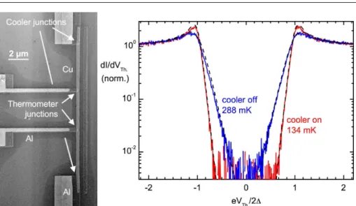
Fig. 2 (Color online) Left: Scanning electron micrograph of a micro-cooler with an external thermometer on the central normal metal island (Sample A). The cooler and the thermometer are made of two Al-AlO(x)-Cu junction in series. The area of thermometer junctions is 0.3 µm × 0.3 µm and that of cooler junctions is 1.5 µm × 0.3 µm. The central normal metal island is 14 µm long, 0.3 µm wide and 50 nm thick. Right: Sample A thermometer differential conductance versus voltage for two different cooler voltage biases. The state for zero cooler bias is called ”cooler off”. A cooler bias of 0.308 mV defines the ”cooler on” state. The dashed lines are fits to the Eq. 1. The cryostat temperature is 275 mK and the gap is ∆ = 0.46 mV.
temperature. For kBTe ≪ ∆, the Fermi-Dirac function can be approximated by an
exponential and the current through the N-I-S junction is then [5]:
I(V ) ≃ I0exp[eV − ∆ kBTe ], with I0= ∆ eRn r πkBTe 2∆ . (3)
This means that, in a logarithmic scale, the slope of the differential conductance dI/dV versus the bias voltage V plot is inversely proportional to the electron temperature. The horizontal dotted line on Fig. 1 illustrates that when biasing the junction at a constant current, measuring the voltage gives directly the electronic temperature in the normal metal. Since Rnand ∆ are obtained from the experiment, there is no free
fitting parameter involved. Voltage-biasing the junction and measuring the current provides the same type of information.
Fig. 2 left part shows the design of the first set of devices we have studied. The central normal metal (Cu) island is connected to two superconducting (Al) reservoirs through tunnel barriers of 0.3 × 1.2 µm2 large area (top and bottom of Fig. 2 left part). This S-I-N-I-S junction is called the ”cooler junction”. The two 40 nm thick and 1.5 µm wide superconducting Al electrodes were in-situ oxidized in 0.2 mbar of oxygen for 3 min before the deposition of the central Cu island that is 14 µm long, 0.3 µm wide and 50 nm thick. The normal metal island has two additional small Al junctions on it (left of the image) with an area of 0.3 × 0.3 µm2. These two junctions constitute a S-I-N-I-S thermometer.
Fig. 2 right part shows the thermometer differential conductance versus voltage at two different cooler voltage biases Vcooler. Both data are fitted with Eq. 1 (dashed
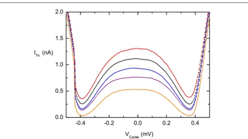
Fig. 3 (Color online) Sample A thermometer current versus cooler bias voltage for different base temperatures. From top to bottom, the cryostat temperature is 345, 325, 275, 306, 285 mK. The thermometer is voltage biased at 0.35 mV.
lines). In the ”cooler off” state defined by Vcooler= 0, the fitted normal metal electron temperature is 288 mK, which is close to the measured cryostat temperature. This agreement shows the good thermalization of the normal metal electrons to the cryostat temperature. In the ”cooler on” state, the cooler junction is biased near the optimum voltage, Vcooler= 0.308 mV. The same fitting procedure provides a normal metal
elec-tron temperature of 134 mK. This experiment illustrates that elecelec-tron cooling can be accurately detected with a S-I-N-I-S thermometer. The quality of the fits is consistent with a thermal quasi-equilibrium of the electron population in the metal. Here, the electrons in the metallic island have cooled from the cryostat temperature of 288 mK down to 134 mK.
Fig. 3 shows the measured thermometer current as a function of the cooler bias for cryostat temperatures from 275 to 345 mK, at a fixed thermometer voltage bias of 0.35 mV. The thermometer current decreases as the cooler bias increases towards its optimum bias, which indicates the cooling of the normal metal electrons. Further increase of the cooler bias injects hot quasi-particules in the normal metal, which heats it, as shown by the increase in the thermometer current.
S-I-N-I-S thermometers have been used in a variety of situations. Nahum et. al. [1] used it to show the first electronic cooling of a Cu island in a micro-cooler. Recently, N-I-S thermometer have been embedded in a LC resonant cicuit to achieve a sub-µs readout time [6]. The proximity effect near a S-N transparent junction is another possibility to measure the local electronic temperature [7]. In the following, we propose a new concept to extract the electronic temperature in the context of S-I-N-I-S micro-coolers.
2 Experimental results in S-I-N-I-S micro-coolers
In the previous section, we used an additional double N-I-S junction as a thermometer to obtain the temperature of the cooled normal metal electrons. However, such a
ther-Fig. 4 (Color online) Left: Scanning electron micrograph of a cooler with no external ther-mometer on the central Cu island (Samples B and C). The cooler is made of two Al-AlO(x)-Cu junctions in series. The area of a cooler junction is 1.5 µm × 0.3 µm. In addition to the cooler, one of the three Al-AlO(x)-Cu probe junctions on the bottom superconducting electrode is visible. Right: Sample B differential conductance data obtained from the cooler and probe junctions at the cryostat temperature of 278 mK. Top curve: the full line shows the character-istic curve obtained from the probe junction and the dotted line is the calculated isotherm with Rn = 5.7 kΩ; ∆ = 0.22 meV. Bottom curve: cooler junction data (full black line) compared with the calculated isotherm at Te= 300 mK with Rn= 2.8 kΩ; 2∆ = 0.42 meV (red dotted line). The green dotted nicely fitting the cooler characteristic is the fit with the thermal model in the device [8]. The voltage is normalized to ∆ (top curve) and 2∆ (bottom curve).
mometer complicates the design and may inhibit a better understanding of the cooling behaviour. In this section, we will discuss the experiments done on a design with no external thermometer. As will be discussed afterwards, the electronic temperature will be obtained directly from the current voltage characteristic of the cooling junction.
Fig. 4 shows the scanning electron micrograph of one cooler device, where the cen-tral Cu island is attached to two superconducting reservoirs through tunnel junctions. The two 40 nm thick and 1.5 µm wide superconducting Al electrodes were in-situ ox-idized in 0.2 mbar of oxygen for 3 min before the deposition of the central Cu island which is 5 (sample B) or 4 µm (sample C) long, 0.3 µm wide and 50 nm thick. In comparison with sample A, the Cu island is shorter while the cooler junctions area is the same, which leads to a more efficient surface/volume ratio in terms of electron cooling. In addition to these cooler junctions, we added three Cu tunnel probes of area 0.3 × 0.3 µm2 on one Al electrode. Due to the large volume of the probe Cu island, the probe is strongly thermalized to the cryostat temperature.
We have measured the current-voltage characteristic across either the cooler or the probe junction. The differential conductance for every junction is then numerically obtained. Fig. 4 shows in a logarithmic scale the differential conductance obtained from the cooler junction and one of the probe junction at a 278 mK cryostat temperature. The voltage axis is normalized to ∆ (probe) or 2∆ (cooler) in order to nicely superpose the two curves. The probe junction characteristic shows the expected linear behavior
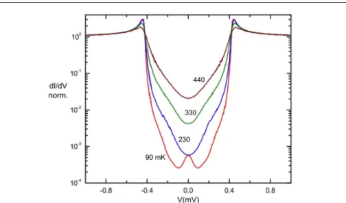
Fig. 5 (Color online) Sample C normalized differential conductance as a function of voltage bias of the cooler junction at the cryostat temperatures of 90, 230, 330 and 440 mK. The normal metal island is 4 µm long, 0.3 µm wide and 50 nm thick. The normal state resistance is RN = 1.9 kΩ.
for a quasi-equilibrium of the normal metal electrons. The data is fitted (dotted line) by an isotherm obtained from Eq. 1 and at Te= 300 mK close to the cryostat temperature.
Here an isotherm means that the electron distribution is at thermal equilibrium and thus given by Fermi distribution function.
In contrast, the isotherm does not fit the characteristic obtained from the cooler junction. The experimental data and the calculated isotherm coincide only at zero bias for sub gap bias. This is expected, since at zero bias there is no heat current due to tunneling, so that the electrons remain thermalized to the cryostat temperature. In the sub-gap region, the differential conductance of the cooler is smaller than the isotherm prediction. This demonstrates the cooling of the electronic population in the normal metal.
Fig. 5 shows the differential conductance obtained from the cooler at different cryostat temperature, down to 90 mK [9]. Again, all the plots are on a logarithmic scale. As expected, the differential conductance at zero voltage bias decreases as the base temperature of the cryostat decreases. However, at very low temperature, the differential conductance at zero bias does not decrease further and even increases as temperature is decreased. This zero bias anomaly (see the T = 90 mK curve in Fig. 5) cannot be explained by any ohmic leakage through the tunnel junctions, since such a leakage would give a constant background in the differential conductance plot. The same behavior was obtained in the probe junctions.
3 The electron energy distribution under tunneling-based cooling
A normal metal cooled by electron tunneling is in principle in an out-of-equilibrium situation. The normal metal states are populated due to the electrons coming from the left superconducting electrode and depopulated by the right electrodes. The
electron-temperature Te will be higher than the phonon temperature. A hot electron regime
is then achieved [10, 11]. In superconducting micro-coolers, heat is extracted from the normal metal electron population and a cold electrons regime is achieved. In every case, the temperature difference between electrons and phonons is of the order of P/ΣU T4 where P is the power, Σ is the electron-phonon constant, U the metal volume.
In the following, we will solve the kinetic balance equation in the normal metal island to determine in a general way the electron energy distribution fN. We will follow the description of Ref. [12] to describe an electron distribution in the normal metal island of a S-I-N-I-S junction. We assume identical tunnel barriers and superconductors on either side of the superconductor. It is also assumed that the superconducting electrodes remain at thermal equilibrium so that the electron energy distribution is given by a Fermi-Dirac distribution fo at a temperature TS.
The tunnel current from the superconductor to the normal metal (in a S-I-N-I-S junction) can be written as:
I(V ) = 2 eRN
Z ∞
−∞
NS(E − eV /2)[f0(TS, E − eV /2) − fN(E)]dE. (4)
Here V is the voltage across, and RN is the resistance of, the two N-I-S junctions
in series. The rate of population of a certain energy level due to injection from the superconductor to the normal metal is given by:
2
RNNS(E − eV /2)[f0(TS, E − eV /2) − fN(E)], (5) and the rate of depopulation of the energy level due to the extraction is given by:
2
RNNS(E + eV /2)[fN(E) − f0(TS, E + eV /2)]. (6) In a relaxation time approximation, the inelastic relaxation of the injected quasiparti-cles at a certain energy level E is given by:
ALNN(E)e2
fN(E) − f0(Te, E)
τE
for plot: Te= 0, ∆ = 0.21 meV.
where A, L are the cross-section and the length of the normal metal, NN is the
non-normalized density of electronic states, and τEthe electron energy relaxation time. Here
we assume that the electron energy relaxation in the normal metal can be considered as a coupling to a thermal bath at an effective temperature Te. This temperature Teis
thus the temperature that the electron population would reach if the energy relaxation is strong enough. For instance, in the case of a dominating electron-phonon coupling, Tewould be equal to the phonon temperature.
At steady state, Eq. 5 = Eq. 6 + Eq. 7. Thus we get:
fN(E) = NS(E −eV2 )f0(TS, E −eV2 ) + NS(E +eV2 )f0(TS, E +eV2 ) + f0(Te,E) τEΓ NS(E −eV2 ) + NS(E +eV2 ) +τE1Γ , (8) where the quantity Γ given by:
Γ = 2
NN(EF)RNALe2 (9)
can be understood physically by noting that Γ−1
is the mean residency time of an electron in the normal metal.
Eq. 8 agrees with the one obtained by J. P. Pekola et. al in Ref. [13] for completely equilibrium distribution in N-metal. Eq. 8 describes a crossover from complete non-equilibrium to non-equilibrium distribution depending on the thermalization of the injected electrons in the central metallic island. If τEΓ << 1, the normal metal electrons follow
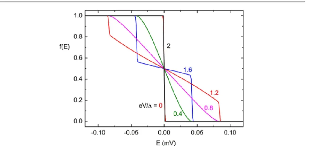
a Fermi distribution function. For τEΓ >> 1, the distribution function in the normal metal is different from the equilibrium Fermi distribution function. Fig. 6 displays the distribution function in this limit for different biases and at zero electronic temperature. The broadening of the distribution function up to eV/∆ = 1 and its sharpening for higher bias can be observed.
The current through the N-I-S junction is obtained by substituting Eq. 8 in Eq. 4. Fig. 7 left part displays the differential conductance versus the voltage bias for both complete equilibrium (τEΓ → 0) and full non-equilibrium (τEΓ → ∞) distribution in
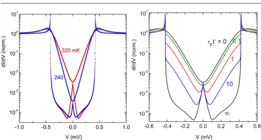
Fig. 7 (Color online) Left: Calculated differential conductance versus voltage bias plot for a complete non-equilibrium (τEΓ → ∞, lower curve at small bias) and a complete equilibrium (τEΓ →0, upper curve at small bias) distribution function in the normal metal at the tem-peratures of 320 and 240 mK. At a given temperature, the two curves coincide at zero bias. The superconducting gap is ∆ = 0.21 meV. Right: Calculated differential conductance versus voltage bias plot for different ratios of the relaxation rate to the injection rate in the normal metal. From bottom to top, the lines correspond to τEΓ = ∞ (black), 10 (blue), 1 (red), 0.1 (green) and 0 (completely thermalized case, black). The parameters are ∆ = 0.21 meV, TS= 320 mK.
the normal metal at two different electronic bath temperatures. In the non-equilibrium case, there is a clear peak in the differential conductance near zero bias. Fig. 7 right part shows the differential conductance isotherm for different τEΓ from 0 to ∞ at T
= 320 mK. As the relaxation time for an electron decreases, the isotherm goes from completely non-equilibrium to quasi-equilibrium distribution in the central metallic island. In every case, the calculated non-equilibrium differential conductance is always below the thermal equilibrium regime one. For τEΓ << 0.1, it is extremely difficult to
distinguish the quasi-equilibrium curve from the fully isotherm curve.
A behavior similar to Fig. 7 was observed in Ref. [13] experiments and discussed partly in terms of out-of-equilibrium effects. In the following, we will argue and present evidence, which shows that our experiments are not in this regime and that the electrons in the cooling metallic island are at quasi-equilibrium.
Comparing our experimental data to the theoretical predictions implies the deter-mination of the physical parameters of our samples. The normalized density of states is given by NN(EF) = (2mkF)/(2h2π2). In sample B, we have RN/2 = 1.4 kΩ; kF =
1.75 × 10¹⁰ m−1; A.L = 5 × 0.3 µm2× 50 nm. We thus find Γ to be of the order of 107s−1
in our samples. As Γ is directly proportional to the the junction conductance, it would be much higher in the case of a S-N-S junction with transparent interfaces.
The inelastic time of scattering in the normal metal can be estimated separately by the weak localization correction to the resistance. We have performed magneto-resistance measurements on a copper wire made with the same source used for making our micro-coolers samples. The copper is of purity 6N (99.9999 percent). The phase coherence time τφ is obtained by fitting the data using weak localisation theory. We
(ii) there are no leakage channels through the junction and no energy states within the superconducting gap; (iii) higher order tunneling processes can be neglected. In the following, we will discuss in detail these assumptions.
Asymmetric tunnel junctions. The central normal metal island is connected to superconducting reservoirs via two tunnel barriers. Although the two barriers are made at the same time, they can be slightly different from each other due for example to a different area. Let Rn1 and Rn2 be the normal state resistances of the two N-I-S
junctions so that the total tunnel resistance across the device is Rn = Rn1 + Rn2.
The junction asymmetry is then defined by the ratio x = Rn1/Rn2. The total current
across the S-I-N-I’-S junction is given by:
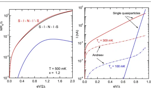
I(V ) = 1 eRn 1 + x 2x Z ∞ 0 NS(E)[fN(E − 2x 1 + x eV 2 ) − fN(E + 2x 1 + x eV 2 )]dE. (10) Fig. 8 shows the comparison of the calculated current-voltage characteristic for a sym-metric and an asymsym-metric junction with x = 1.2. The total current across the junction for low bias voltage is little affected by the asymmetry. This is due to the singularity of the differential conductance at the gap, which regularizes the voltage [16]. The dif-ference in the current is roughly proportional to the asymmetry and it is maximum at the gap voltage. For our samples, the resistance difference between the two junctions is estimated to be less than 5 percent. We consider then that we can neglect the effects of the device assymmetry.
Energy states within the superconductor energy gap.The presence of energy states within the superconductor gap can be described with the help of Dynes parameter η so that [17]:
NS(E) = |Re(p E + iη
(E + iη)2+ ∆2)|. (11)
The effect of taking into account a significant Dynes parameter is to smear the differential conductance curve as a function of voltage and therefore increase the con-ductance at zero bias. In the case of bulk Al, there is no justification for taking a significant Dynes parameter. Fig. 5 shows that the differential conductance at inter-mediate temperature (above 250 mK) is definitely not influenced by a possible Dynes parameter since the differential conductance in this temperature range coincides with expectation and is also higher than the one observed at lower temperature (90 mK).
Fig. 8 (Color online) Left: The top two curves display the calculated normalized current -voltage characteristics of a non-symmetric S-I-N-I’-S (x = 1.2) and a symmetric S-I-N-I-S junction. The bottom curve displays the current difference as a function of voltage. Right: Calculated current contributions as a function of the voltage of a N-I-S junction at Te= 300 and 100 mK. The full lines show the contribution due to the single quasiparticle current and the dotted lines show the contribution of the phase-coherent Andreev current. The parameters are ∆ = 0.225 meV, Rn= 2 kΩ and Lϕ= 1.5 µm.
As already mentioned, a leakage in our tunnel junctions cannot explain the observed behavior with a differential conductance peak at zero bias.
Tunnel current due to higher order processes.The tunneling of single-particles gives a zero tunnel current for energies below the superconducting gap ∆: only electrons with energy E > ∆ contribute to the current across the N-I-S junction. However, higher order tunnel processes do contribute to the current at an energy below the superconducting gap. The second order tunneling process is the Andreev reflection [18, 19], which allows the transfer of two electrons with E < ∆ from N to form a Cooper pair in S. The reverse process is also possible and corresponds to the creation of Andreev pairs [20] in the normal metal.
The amplitude of the Andreev reflection current vanishes with the transparency of the junction in the ballistic regime [21]. However, confinement by the disorder in the electrode leads to the coherent addition of the many individual transmission prob-abilities for the transfer of a 2e charge, resulting in the enhancement of the sub-gap conductivity [22, 23, 24]. Fig. 8 right part shows the calculated current voltage char-acteristic of a N-I-S junction at two different temperatures and for a transparency of 10−5
similar to the ones of our samples. Here we have used the theory of Ref. [24] in the 1D limit. The respective contributions of the single quasiparticle current and the phase coherent Andreev current are displayed. At moderate temperatures (see the 300 mK curve), the contribution due to Andreev current is found to be negligibly small in comparison with the single quasiparticle tunnel current. This does not hold at low enough temperatures, as is illustrated by the 100 mK curves of Fig. 8 right part [9].
In conclusion for this section, we have examined the different assumptions required to consider that the current through our S-I-N-I-S micro-coolers is related solely to
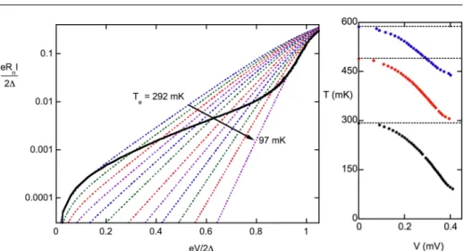
Fig. 9 (Color online) Left: Sample B experimental current-voltage characteristic at a 275 mK cryostat temperature (full line, black) superposed on a series of calculated isotherm character-istic following Eq. 1 from T = 292 mK (top) to T = 97 mK (bottom). Every crossing point gives the electronic temperature Te in the central normal metal metal at a particular bias. Right: Sample B normal metal electronic temperature as a function of the cooler bias at a cryostat temperature of 275, 470 and 570 mK. The base temperature extracted from the data is 292, 489 and 586 mK respectively.
single-particle tunneling and thus follows Eq. 1. We conclude that they are correct in the intermediate temperature regime, which in our case corresponds to T > 250 mK.
5 Extraction of the electron temperature
The above statement allows us to extract the temperature Te(V ) in the sub-gap region
by comparing our experimental current-voltage characteristic to a series of theoretical isotherm curves obtained from Eq. 1.
Fig. 9 left part shows the current voltage characteristic of the cooler junction at the cryostat temperature of 300 mK along with the simulated isotherms. At zero bias, there is a good overlap between the experiment (black complete line) and the isotherm cor-responding a 292 mK electron temperature. As the cooler bias increases, the isotherm no longer follows the experiment and there is a crossover with the next isotherm at a slightly lower temperature, and so on. At the gap, electrons in the metal island have cooled from the base temperature of 292 mK to 97 mK. Here the normal state con-ductance for the S-I-N-I-S cooler of 2.8 kΩ and the gap 2∆ = 0.428 meV necessary for the isotherms calculations were obtained from the differential conductance plot.
It is interesting to note that such an extraction of the electron temperature cannot be done on a differential conductance-bias plot like Fig. 4. As the tunneling current is a function of both bias and temperature, the full derivative gives:
dI dV = ∂I(V, T ) ∂V + ∂I(V, T ) ∂T dT dV (12)
Neglecting the second part on right side of the above equation would generate a system-atic error in determining the electron temperature from the differential conductance.
higher ratio of volume/area of N-metal in comparison with previous design, which can contribute to a better cooling of the island.
Acknowledgements We acknowledge the financial support from the ANR contract ”Elec-EPR”, the ULTI-3 and NanoSciERA ”Nanofridge” EU projects. H. Courtois thanks the Low Temperature Laboratory for hospitality. We thank E. Favre-Nicollin and P.S. Luo for their contribution in the early stages of this work.
References
1. M. Nahum, T. M. Eiles and John M. Martinis, Appl. Phys. Lett. 65, 3124 (1994). 2. J. P. Pekola, D. V. Anghel, T. I. Suppula, J. K. Suoknuuti, A. J. Manninen, and M.
Manninen, Appl. Phys. Lett. 76, 2782 (2000).
3. J. M. Rowell and D.C. Tsui, Phys. Rev. B 14, 2456 (1976). 4. M. Nahum and J. M. Martinis, Appl. Phys. Lett. 63, 3075 (1993)
5. L. Solymar, Superconductive Tunneling and Applications, Wiley Intersciences, New York, 1972.
6. D. R. Schmidt and C. S. Yung, and A. N. Cleland, Appl. Phys. Lett. 83, 1002 (2003). 7. Z. Jiang and H. Lim and V. Chandrasekhar, and J. Eom, Appl. Phys. Lett. 83, 2190 (2003). 8. Sukumar Rajauria, P. S. Luo, T. Fournier, F. W. J. Hekking, H. Courtois, and B. Pannetier,
Phys. Rev. Lett. 99, 047004 (2007).
9. Sukumar Rajauria, P. Gandit, T. Fournier, F. W. J. Hekking, B. Pannetier, and H. Courtois, Phys. Rev. Lett. 100, 207002 (2008).
10. M. L. Roukes, M. R. Freeman, R. S. Germain, R. C. Richardson, and M. B. Ketchen, Phys. Rev. Lett. 55, 422 (1985).
11. F. C. Wellstood, C. Urbina, and J. Clarke, Phys. Rev. B 49, 5942 (1994). 12. D. R. Heslinga and T. M. Klapwijk, Phys. Rev. B 47, 5157 (1993).
13. J. P. Pekola, T. T. Heikkil¨a, A. M. Savin, J. T. Flyktman, F. Giazotto, and F. W. J. Hekking, Phys. Rev. Lett. 92, 056804 (2004).
14. B. Pannetier, J. Chaussy, and R Rammal, Phys. Rev. B 68, 085413 (2003).
15. F. Pierre, A. B. Gougam, A. Anthore, H. Pothier, D. Est´eve, and O. Norman Birge, Phys. Rev. B 68, 085413 (2003).
16. J. P. Pekola, A. J. Manninen, M. M. Leivo, K. Arutyunov, J. K. Suoknuuti, T.I. Suppula, and B. Collaudin, Physica B 280, 485 (2000).
17. R. C. Dynes, J. P. Garno, G. B. Hertel, T. P. Orlando, Phys. Rev. Lett. 53, 2437 (1984). 18. A. F. Andreev, Zh. Eksp. Teor. Fiz. 46, 1823 (1964).