HAL Id: hal-00748983
https://hal.archives-ouvertes.fr/hal-00748983
Submitted on 6 Nov 2012HAL is a multi-disciplinary open access archive for the deposit and dissemination of sci-entific research documents, whether they are pub-lished or not. The documents may come from teaching and research institutions in France or abroad, or from public or private research centers.
L’archive ouverte pluridisciplinaire HAL, est destinée au dépôt et à la diffusion de documents scientifiques de niveau recherche, publiés ou non, émanant des établissements d’enseignement et de recherche français ou étrangers, des laboratoires publics ou privés.
Fabrication and characterization of high damping
electrostatic micro devices for vibration energy
scavenging
Ghislain Despesse, Thomas Jager, Chaillout Jean-Jacques, Jean-Michel Léger,
Andrea Vassilev, Skandar Basrour, Benoit Charlot
To cite this version:
Ghislain Despesse, Thomas Jager, Chaillout Jean-Jacques, Jean-Michel Léger, Andrea Vassilev, et al.. Fabrication and characterization of high damping electrostatic micro devices for vibration energy scavenging. Proc. Design, Test, Integration and Packaging of MEMS and MOEMS, 2005, pp.386-390. �hal-00748983�
FABRICATION AND CHARACTERIZATION OF HIGH DAMPING ELECTROSTATIC
MICRO DEVICES FOR VIBRATION ENERGY SCAVENGING
G. Despesse*, T. Jager*, J.J. Chaillout*, J.M. Léger*, A. Vassilev*
S. Basrour** and B. Charlot**
*CEA/DRT – LETI/DCIS, 17 rue des Martyrs, 38054 Grenoble Cedex 09, France, despesse@cea.fr
**TIMA, 46 avenue Félix Viallet, 38031 Grenoble Cedex, France
ABSTRACT
Advances in low power electronics and microsystems design open up the possibility to power small wireless sensor nodes thanks to energy scavenging techniques. Among the potential energy sources, we have focused on mechanical surrounding vibrations. To convert vibrations into electrical power we have chosen mechanical structures based on electrostatic transduction. Thanks to measurements and in agreement with recent studies [1], we have observed that most of surrounding mechanical vibrations occurs at frequencies below 100 Hz. We report here global simulations and designs of mechanical structures able to recover power over a large spectrum below 100 Hz. Contrary to existing structures tuned on a particular frequency [2], we have investigated conversion structures with a high electrical damping. Mathematica analytical models have been performed to determine the mechanical and electrical parameters that maximize the scavenged power for a wide number of applications (Figure 3). Two prototypes of mechanical structures have been designed.
1. INTRODUCTION
Advances in low power electronics and microsystems design open up the possibility to power small wireless sensor nodes thanks to energy scavenging techniques. Depending on the system environment, many different types of energy sources can be used: thermal, radiative, mechanical or chemical. Among these sources we had to choose one whose conversion system is adapted to size reduction. We finally decided to focus on mechanical surrounding vibrations.. As shown on Figure 1 and Figure 2 and by other recent studies [1], surrounding mechanical vibration frequencies are mainly and widely distributed below 100 Hz.
Figure 1 : Acceleration spectrum on a car
Figure 2 : Acceleration spectrum on a metallic stair
To convert most of these vibrations into electrical power it has been chosen to investigate conversion structures based on electrostatic transduction with high electrical damping. Many advantages are provided by the electrostatic conversion: it is easy to integrate and its power density is increased by the size reduction. Moreover, high electrical dampings are easily achievable through this transduction principle. Thus, and contrary to most of existing systems [1-3], our structures will be able to recover power over a large spectrum below 100 Hz.
2. CONVERSION STRUCTURES 2.1. Choice of the conversion system
In a first step the mechanical behavior of the conversion structure has been approximated through a linear viscous damping model [4]. In function of the input acceleration A, its pulsation , the moving mass m, the resonant pulsation n of the structure and the mechanical
and electrical damping m and e, the maximum
mechanical scavenged power P is given by:
20 40 60 80 Hz 0.05 0.1 0.15 0.2 0.25 0.3 m.s-2 A(f) m.s-2
G. Despesse, T. Jager, S. Basrour, J.J. Chaillout, B. Charlot, J.M. Léger and A. Vassilev
HIGH DAMPING ELECTROSTATIC MICRO DEVICES FOR VIBRATION ENERGY SCAVENGING
(
)
2 2 2 2 3 21
2
−
+
+
=
n n m e n n n emA
P
ω
ω
ω
ω
ζ
ζ
ω
ω
ω
ω
ζ
(1)We can easily see that the scavenged power is directly proportional to the moving mass and to the square of the input acceleration. An operation with a high electrical damping has been chosen to maximize the scavenged power for a wide number of applications (i.e. over a large frequency band) neglecting the mechanical damping compared to the electrical one.
For all types of existing electrostatic microstructures (out-of-plane gap closing, in-plane overlap or in-plane gap closing [2]) and their operating cycles (voltage-constrained or charge-(voltage-constrained cycle [3]), the electrical damping is due to the electrostatic force Fe appearing between two mechanical parts (the moving mass and fixed electrodes) set at different potentials. For a high damping configuration, the electrostatic force has to counterbalance almost entirely the mechanical spring force Fm=kz, which is proportional to the relative displacement z and to the mechanical structure stiffness k. In agreement with the electrostatic force characteristics presented in Table 1 in function of the conversion structure and its operation cycle, the most convenient configuration seems to be an in-plane gap closing structure with a charge constrained cycle. For this configuration, the electrostatic force Fe is also proportional to the relative displacement and can be expressed as Fe=kez where ke is defined as the electrical stiffness.
Structure Q constrained V constrained
Out-of-plane Fe constant Fe ~ 1/z In-plane
overlap Fe ~ 1/z2 Fe constant
In-plane gap
closing Fe ~ z Fe ~ 1/z2
Table 1: Electrostatic force variation for different system configurations
A high electrical damping is finally achieved by choosing an electrical stiffness close to the mechanical one.
2.2. Modeling and simulations
Assuming an in-plane gap closing conversion structure operating in a charge cycle, Mathematica analytical models have been performed to determine the
mechanical and electrical parameters that maximize the scavenged power for a wide number of applications. Based on former experimental vibration measurements, the recoverable power and the vibration amplitude have been estimated in function of the resonant frequency for high electrical damping configurations (i.e. ke/k close to 1). These calculations are summarized on Figure 3 for ke/k =0.67.
Figure 3: Recoverable power (a) and vibration amplitude (b) for a 1 g moving mass in function of the
resonant frequency for ke/k=0.67
Combining displacement (<100-150 µm) and scavenged power (>2 µW) constraints a 50 Hz resonant frequency has finally been chosen for our structures.
As shown by Equation (1) the scavenged power is proportional to the moving mass: to scavenge a significant power it has thus been decided to increase the moving mass of our future silicon microstructure by sticking an additional tungsten mass on the moving part. In order to early validate the scavenging electronics principles it has also been decided to realize an intermediate macro prototype in bulk tungsten alloy.
Complementary FEA (Finite Element Analysis) simulations with ANSYS® have also been performed to validate our mechanical designs.
Finally, the scavenged mechanical power was estimated for both prototypes thanks to global simulations whose results are reported in Table 2 along with main prototypes characteristics. 20 40 60 80 100 fr(Hz) 5 10 15 20 25 30 P(µW) Recoverable power Car engine Car driving Drill Metallic stairs 20 40 60 80 100fr(Hz) 50 100 150 200 250 300 µm Displacement Car engine Car driving Drill Metallic stairs
Characteristics Bulk tungsten macrostructure Silicon microstructure Size 18 cm2x1 cm 81 mm2x0.4 mm Moving mass 104 g 2 g Cmin/Cmax 900 / 3590 pF 14 / 147 pF Resonant frequency 50 Hz 50 Hz Maximum displacement 116 µm 95 µm Maximum scavenged power 6 mW 70 µW
Table 2: Characteristics and calculated performances of the prototypes
2.3. Realizations
The macroscopic conversion structure has been realized in bulk tungsten thanks to electrical discharge machining (EDM). This technique is a good compromise to test and validate the electronics principle. The structure is presented on Figure 4.
Figure 4: Bulk tungsten prototype
The second prototype is a silicon one whose realization process is based on Deep Reactive Ion Etching techniques as presented on Figure 5:
Step 1
Step 2
Step 3
Figure 5: Flowchart for the silicon prototype
Flowchart description:
Ü Step 1: Etching of the back face silicon cavity Ü Step 2: Wafer bonding and Aluminium
metallization
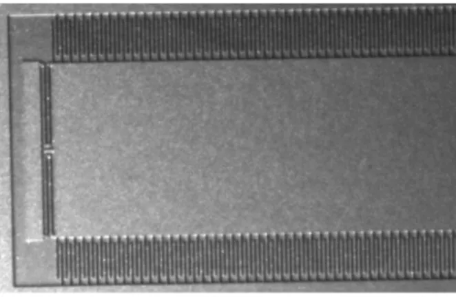
Ü Step 3: DRIE Etching and structure release Many advantages can be achieved with size reduction: a higher capacity range and a higher quality factor with a smaller system size. On the Figure 6 is presented the final structure.
Figure 6: Silicon prototype
The measured resonant frequency of the tungsten prototype is a little lower than 50 Hz and the effective maximum vibration amplitude of its moving mass is limited to 90 µm. This is due to limitations inherent to the EDM process (thin elements can be deformed by the heat released during electrical discharges) combined with the inaccuracies of the final assembling of moving and fixed elements.
Instead of the 6 mW of scavenged power initially expected with a 116 µm maximum displacement at 50 Hz, the maximum expected power at 50 Hz is then reduced to 1.76 mW.
3. CONVERSION AND MANAGEMENT ELECTRONICS
As the variable capacitance structure is driven by mechanical vibrations, it oscillates between a maximum capacitance Cmax and a minimum capacitance Cmin. The
maximum capacitance is variable and depends on the displacement amplitude and Cmin is fixed by the initial
equilibrium position of the structure. For a charge constrained operating cycle a given charge is injected under a initial Vmin voltage on the structure when the
maximum of capacitance is reached. An electrostatic force appears and absorbs a part of the mechanical movement until the structure reaches its equilibrium
G. Despesse, T. Jager, S. Basrour, J.J. Chaillout, B. Charlot, J.M. Léger and A. Vassilev
HIGH DAMPING ELECTROSTATIC MICRO DEVICES FOR VIBRATION ENERGY SCAVENGING
position. The injected charge is then recovered under a higher Vmax voltage. The maximum recoverable energy
per cycle is given by:
)
(
max min max minV
C
C
V
E
=
−
2
1
(2)To observe the influence of the effective movement amplitude on the capacitance and the voltage variations, the response to a decreasing sinusoidal movement has been simulated for an arbitrary structure size. Results are presented on Figure 7.
Figure 7: Charge-constrained cycle operation
As the vibration amplitude decreases, the difference between the charge and discharge energy decreases, as does the converted energy.
An efficient detection of maximum and minimum of capacitance is needed to work properly. A driving circuit between the storage unit and the variable capacitance is also required for the charge and the discharge.
3.1. Detection of capacitance extrema
The capacitance extrema detection can be achieved by injecting a known high frequency current in the variable capacitance: the capacitance can be measured by filtering or/and by using a synchronous detection. Unfortunately the power consumption of circuits based on this operating
principle is too high. Instead of measuring the capacitance value we therefore focused on the measurement of the capacitance voltage derivative. However this solution works only if there is always a residual charge on the variable capacitance: instead of entirely discharging the capacitance at every cycle, the discharge will not be totally completed.
With this residual charge on the variable capacitance, a first extremum of the capacitance voltage is achieved when the capacitance is maximum. An additional effective charge is then loaded on the capacitance. When the capacitance becomes minimal, the voltage is maximum and reaches a second extremum: the capacitance is almost entirely discharged and a new conversion cycle starts.
3.1. Power management
Controlled by the detection stage, the charge and the discharge of the variable capacitance are achieved through a Flyback structure presented on Figure 8:
Figure 8: Flyback power structure
This structure has many advantages. The first one is that the storage unit side could be easily integrated (voltage lower than 5 V). Only one transistor (Ks) is still subjected to high voltage: the leakage current losses and the parasite capacitance losses are limited.
The second one is that the number of turns on each side of the magnetic circuit can be adjusted to have the same switch-on time for both Kp and Ks transistors.
The third advantage is that the transistors commands are referenced to the same ground potential.
To charge the variable capacitance, the transistor Kp is switched on long enough for the magnetic circuit to be loaded with the requested energy. This energy is then transferred in the variable capacitance when Kp and Ks are respectively switched off and on: Ks is kept on until the magnetic circuit is entirely discharged in the variable capacitance.
To discharge the variable capacitance, Ks is first switched on to transfer the capacitance energy in the magnetic circuit. Then, Kp and Ks are respectively switched on and off and the energy is transferred from the magnet circuit into the storage unit.
z
(t)
moving part fixed part 0.01 0.02 0.03 0.04 t(s) -20 -10 10 20 µm Relative displacement 0.01 0.02 0.03 0.04 t(s) 50 100150 pF Variable capacity's value
0.01 0.02 0.03 0.04 t(s)
1 2 3
nC Variable capacity's charge
0.01 0.02 0.03 0.04 t(s)
40 80
120 V Variable capacity's voltage
E
C
L
pL
sKp Ks
Vc
Apart from the charge and the discharge, Kp and Ks are kept open.
Experimental measurements of this charge and discharge cycles on the bulk tungsten macrostructure are reported on the Figure 9. These measurements are in good agreement with simulations.
Figure 9: Charge and discharge cycle for a 30 Hz sinusoidal mechanical excitation.
Experimental charge and discharge times have been measured in the µs range: as expected they are negligible compared with the mechanical cycle period (in the ms range).
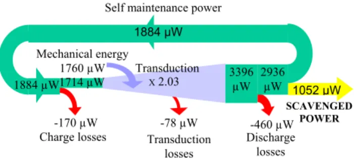
3.1. Power balance and conversion efficiency
All parasitic losses associated to the magnetic circuit and the transistors have been taken in account to estimate the power balance of the global system presented in Figure 10 for the tungsten prototype.
These parasitic elements have been measured and then implemented in modeling to simulate the loss repartition. Once these elements taken into account, simulations are in good agreement with measurements. The power balance is almost proportional to the mechanical frequency and is strongly linked to the relative displacement amplitude. For the tungsten prototype, the power balance becomes positive for vibration amplitudes higher than 60 µm.
As presented on Figure 10 for a vibration amplitude of 90 µm at 50 Hz, the global scavenged power is about 1052 µW with an absorbed mechanical power of about 1760 µW. The global efficiency is thus close to 60 %.
Figure 10: Power balance for the tungsten prototype (50 Hz; vibration amplitude of 90 µm)
With size-reduction we can expect an higher conversion efficiency due to a better mechanical accuracy and a higher quality factor in the silicon prototype realization.
4. CONCLUSION
Global simulations have been performed on a high damping electrostatic system for vibration energy scavenging. A macrostructure in bulk tungsten and a silicon microstructure have been designed along with the associated management electronics. In agreement with simulations, 1mW of scavenged power is already delivered by the tungsten prototype with a global conversion efficiency of 60 % submitted to a sinusoidal vibration amplitude of 90 µm at 50 Hz. In situ measurements have also been performed and up to 250 µW have been scavenged on a car engine. First conversion results with the silicon microstructure are expected soon and shall be about a few ten µW.
5. REFERENCES
[1] S. Roundy, P. K. Wright, and J. Rabaey, "A study of low level vibrations as a power source for wireless sensor nodes", Computer Communications, vol. 26, 1131-1144, 2003.
[2] S. Roundy, P. K. Wright and K. S. J. Pister, "Micro-Electrostatic Vibration-to-Electricity Converters", Proceedings of IMECE2002, 1-10, 2002.
[3] S. Meninger, "A Low Power Controller for a MEMS Based Energy Converter", Master of Science at the Massachusetts Institute of Technology, 1999.
[4] C. B. Williams and R.B Yates, "Analysis of a micro-electric generator for microsystems", Proceedings of the Transducers 95/Eurosensors IX, 369-372, 1995. 2.5 5 7.5 10 12.5 t(ms) 50 100 150 200 250 300 Vc(t) Vc(V) Simulation Measurement 4 8 12 t 50 100 150 200 250 300 Vc (µs) -4 4 8 t 50 100 150 Vc (µs) 1052 µW 1884 µW SCAVENGED POWER
Self maintenance power
2936 µW -460 µW Discharge losses 3396 µW -170 µW Charge losses X 2.03 -78 µW Transduction losses 1884 µW Transduction Mechanical energy 1760 µW 1714 µW