HAL Id: hal-02066472
https://hal.archives-ouvertes.fr/hal-02066472
Submitted on 13 Mar 2019
HAL is a multi-disciplinary open access
archive for the deposit and dissemination of
sci-entific research documents, whether they are
pub-lished or not. The documents may come from
teaching and research institutions in France or
abroad, or from public or private research centers.
L’archive ouverte pluridisciplinaire HAL, est
destinée au dépôt et à la diffusion de documents
scientifiques de niveau recherche, publiés ou non,
émanant des établissements d’enseignement et de
recherche français ou étrangers, des laboratoires
publics ou privés.
Light emission and structure of Nd-doped Si-rich-HfO 2
films prepared by magnetron sputtering in different
atmospheres
Leonardo Gabriel Vega Macotela, Vega Macotela, Tetyana Torchynska, Larysa
Khomenkova, Fabrice Gourbilleau
To cite this version:
Leonardo Gabriel Vega Macotela, Vega Macotela, Tetyana Torchynska, Larysa Khomenkova, Fabrice
Gourbilleau. Light emission and structure of Nd-doped Si-rich-HfO 2 films prepared by magnetron
sputtering in different atmospheres. Materials Chemistry and Physics, Elsevier, 2019, 229, pp.263-268.
�10.1016/j.matchemphys.2019.03.007�. �hal-02066472�
Light emission and structure of Nd-doped Si-rich-HfO
2
films prepared by
magnetron sputtering in di
fferent atmospheres
Leonardo Gabriel Vega Macotela
a, Tetyana Torchynska
b,∗, Larysa Khomenkova
c,d,e,
Fabrice Gourbilleau
daInstituto Politécnico Nacional - ESIME, México City, 07738, Mexico bInstituto Politécnico Nacional - ESFM, México City, 07738, Mexico
cV. Lashkaryov Institute of Semiconductor Physics at the NAS of Ukraine, 45 pr. Nauky, Kyiv, 03028, Ukraine dCIMAP, UMR CNRS/CEA/ENSICAEN/UNICAEN, 6 Boulevard Maréchal Juin, 14050, Caen Cedex 4, France eNational University“Kyiv-Mohyla Academy”, 2 Skovorody str., Kyiv, 04170, Ukraine
A B S T R A C T
Radio-frequency magnetron sputtering was used to produce HfO2films doped with Nd, Si and N. The deposition was carried out in two different atmospheres: i) in pure argon plasma to grow Si-HfO2:Ndfilms, and ii) in argon-nitrogen mixed plasma to produce Si-N-HfO2:Ndfilms. The effect of annealing temperature on optical and structural properties of the films was investigated. Annealing was performed at TA= 800–1100 °C for tA= 15 min in nitrogen atmosphere. The evolution offilm's properties was studied by means of the scanning electronic microscopy (SEM), energy dispersive X-ray spectroscopy (EDS), X-ray diffraction (XRD) and photo-luminescence (PL) methods. It was observed that thefilm morphology depends significantly on the deposition atmosphere. For the Si-HfO2:Ndfilms, the presence of the grains with the mean size about 100 nm was detected by the SEM method. The tetragonal HfO2and SiO2phases have been detected by the XRD method afterfilm annealing at 950 °C. PL spectra of thesefilms are complex and demonstrate several PL bands in the visible (400–750 nm) and infrared (800–1430 nm) spectral ranges. Their contribution depends on the annealing tem-perature and governs the shape of total PL spectrum. In contrary, the Si-N-HfO2:Ndfilms showed unstructured smooth surface as well as featureless PL spectra. Whatever the annealing temperature, they demonstrate broad unstructured PL band with the peak within 440–480 nm. Peculiarities of PL spectra of both types of the films and the mechanism of phase separation are analyzed and discussed.
∗Corresponding author.
E-mail address:ttorch@esfm.ipn.mx(T. Torchynska).
1. Introduction
HfO2-based materials during the last decades are mainly considered
as the alternative gate dielectrics to silicon oxide in complementary metal-oxide semiconductor technology. At the same time, their high refractive index (n = 1.9–2.2, depending on preparation method), high optical transparency in the ultraviolet-infrared spectral range (band gap is about 5.8–6.0 eV), compactness and hardness offer optical applica-tions as well. The phonon cut-off energy (∼about 780 cm−1) reduces
the probability of non-radiative phonon assisted relaxation that is at-tractive for doping these materials in particular with the rare-earth elements [1–3]. However, in spite of mentioned advantages, the HfO2
-based compounds up to now are not often addressed as a host for the rare-earth ions. Just a few groups reported on the light emission ob-tained from Eu3+-doped HfO2-based nanotubes [4], Er3+-doped sol-gel
SiO2-HfO2waveguides [5–7], as well as Er3+or Pr3+doped HfO2-based
thinfilms [8,9].
Among different rare-earth ions, the trivalent neodymium (Nd3+
) was used in the inorganic laser materials attracting the great attention of scientific researches and industrial applications. Nd3+ions exhibit
broad and strong absorption band around 800 nm and a very intense emission in the near-infrared luminescence range from 800 to 1430 nm associated with the4F
3/2→4IJ(J = 9/2, 11/2, 13/2) optical transitions
in the 4f inner electronic shell of Nd3+ions, following a known “four-level” scheme [10,11]. The4F
3/2emitting state can be populated
con-veniently by the emission of low-cost commercially available laser diodes. In addition, it has many intense pumping levels and efficient up-converted emissions [11]. Among different host matrix materials, the garnets [10], glasses [12], ceramics [13], II-VI compounds [14], as well as Si-rich SiO2or Si3N4are the most studied [15,16].
In this work we present the results of the structural and spectro-scopic study of HfO2-based thinfilms co-doped with Si, N and Nd grown
by radio frequency (RF) magnetron sputtering. The effect of annealing temperature on the phase separation process and luminescence of such composite films is considered as a fruitful way for monitoring the properties of these materials.
2. Experimental details
Thefilms were grown by RF magnetron sputtering on 2-inch, B-doped, (100) oriented Si wafers with a resistivity of about 15Ω cm. Prior to the deposition, the substrates were submitted to standard RCA cleaning: dipped in a diluted hydrofluoric solution (10%), dried in N2,
and immediately transferred to the load-lock vacuum chamber of the deposition setup. A pure HfO2target (99.9%) topped with the
cali-brated Si and Nd2O3pellets was used. The Si and Nd2O3pellets covered
about 16% of target surface each.
To produce the Si-HfO2:Ndfilms, the deposition was performed in
pure Ar plasma with argonflow fAr= 3sccm (so-called“standard”
ap-proach). The deposition time was 200 min allowed to grow homo-geneousfilm with the thickness of about 410 nm.
The Si-N-HfO2:Ndfilms were produced with Ar-N2mixed plasma
(fAr= 3 sccm and fN2= 2 sccm; so-called “reactive” approach). The
deposition time was 240 min resulting in the film thickness of about 260 nm.
All other deposition conditions were similar for both approaches, i.e. the RF power density, substrate temperature (TS), total plasma
pressure and substrate-cathode distance were 0.74 W/cm2, 400 °C,
0.03 mbar and 57 mm, respectively. After the film deposition, each substrate was cut onto the smaller pieces (usually 1 × 1 cm2) to study the effect of annealing treatment. It was performed in a conventional horizontal furnace at different temperatures TA= 800–1100 °C during
tA= 15 min in a continuous nitrogenflow (fN2= 48 sccm).
Several experimental techniques were used to analyze the properties of thefilms. The PL emission was excited with a 325 nm line of He-Cd laser or by different lines of Ar+
-ion laser. PL spectra were recorded
using several setups: i) a Jobin–Yvon TRIAX 180 monochromator linked with a fast Hamamatsu photomultiplier and a SRS lock-in amplifier (SP830 DPS) (for 400–1000 nm spectral range); ii) with a Jobin Yvon 1 m single grating monochromator coupled to a Northcoast Germanium detector cooled with liquid nitrogen and a SRS lock-in amplifier (SP830 DPS) (for 800–1700 nm spectral range). Referenced chopping frequency was 20 Hz.
To study the film surface morphology as well as to get the in-formation on their chemical composition, a scanning electronic mi-croscope (SEM) Quanta 3D FEG-FEI with an additional detector Apollo X10 mark EDAX for the energy dispersive X-ray spectroscopy (EDS) was used.
X-ray diffraction (XRD) results were obtained using the equipment of Model X”PERT MRD with the Pixel detector, three-axis goniometry and parallel collimator with the angular resolution of 0.0001°. X-ray beam was achieved from the Cu source (Kα1line,λ = 1.5406 Å). All
experiments were carried out at the room temperature. 3. Results and discussion
3.1. Chemical composition of thefilms
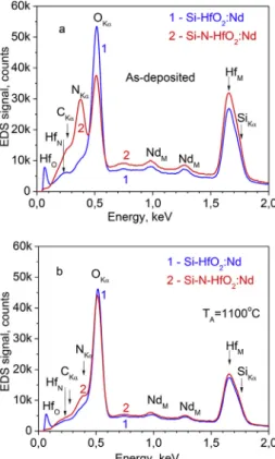
The chemical composition of thefilms was analyzed by energy-dispersive X-ray spectroscopy (EDS). The representative spectra for as-depositedfilms are shown inFig. 1. As one can see, for allfilms, the presence of Hf, Si, O and Nd elements was registered. In addition, for the films deposited in argon-nitrogen plasma, the significant signal from the nitrogen was also detected (Fig. 1a, curve 2). Note that the carbon signal can be due to the carbon adsorption on thefilm surface from an ambient atmosphere.
The annealing treatment results in the variation of chemical com-position of the samples that is more prominent for the Si-N-HfO2:Nd
films. It turned out that the nitrogen-related signal is the most affected. Its intensity changes slightly for TA< 950 °C (not shown) and
de-creases significantly for higher temperatures (TA= 1000–1100 °C)
Fig. 1. EDS spectra for Si-HfO2:Nd (curves 1) and Si-N-HfO2:Nd (curves 2) films, as-deposited (a) and annealed at 1100 °C (b).
(Fig. 1b). This effect can be explained taking into account the results of Ref. [17]. The authors demonstrated that rapid (60 s) thermal annealing at 1000 °C in nitrogen atmosphere of HfSiON thinfilms causes the O and N atomic transport and exchange of the chemical species resulting either in the Si-N or Si-O-N bond formation, as well as in the NO for-mation and its out-diffusion from the samples. Considering the an-nealing conditions used for our Si-N-HfO2:Ndfilms, one can assume
that the similar processes can occur in ourfilms. Since the N-related EDS signal decreases in intensity, one can conclude that NO formation is the main process for the N desorption from the films. It should be noted that EDS spectra of annealed Si-HfO2:Ndfilms were found to be
similar to those of as-deposited ones.
3.2. Surface morphology
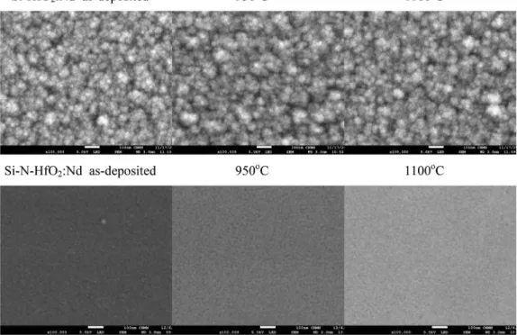
Fig. 2represents the surface SEM images of the Si-HfO2:Nd (Fig. 2,
upper panel) and Si-N-HfO2:Nd (Fig. 2, bottom panel) samples. As one
can see, the morphology of as-depositedfilms depends very much on the sputtering approach. The Si-N-HfO2:Ndfilms, grown with reactive
approach, show smooth surface contrary to their Si-HfO2:Nd
counter-parts deposited in pure argon plasma (Fig. 2). This difference in the film
morphology can be explained taking into account the structure zone model (SZM) proposed in 1969 for thefilms grown by electron-beam plasma vapor deposition [18] and developed later for the sputtering approach [19].
The real structure of the film is determined by four processes: i) shadowing, i.e. a geometric interaction between arriving adatoms and the roughness of the growing surface; ii) surface diffusion, i.e. mobility of adatoms at the surface and interfaces such as grain boundaries; iii) bulk diffusion, i.e. mobility of adatoms in the volume of grains, and iv) recrystallization, i.e. phase transition as a complete change of crystal orientation [18,19]. The processes i) and ii) dominate at low and medium temperature of the substrate, TS, respectively. Processes iii)
and iv) are important at high TS. Besides, process iv) dominates at the
percolation thickness and largefilm thickness.
It was shown that for the most metals and dielectrics, activation energies for diffusion are related to the melting temperature of mate-rial, TM[18]. Thus, the basic processes depend on the TS/TMratio and
determine thefinal structure of the film. In the regard of the value of TS/TM ratio, three different zones were considered: i) when TS/
TM< 0.3, the formation of fine-grained porous structure due to the
low mobility of adatoms and their stick at the place, where they were land on the substrate (zone I); ii) when 0.3 < TS/TM< 0.5, a columnar
structure grows owing to surface diffusion of adatoms with the acti-vation energy of 0.1–0.3 eV (zone II); iii) for TS/TM> 0.5, a rough
equiaxed grain structure appears due to the high bulk diffusion with the activation energy of above 0.3 eV (zone III) [18].
Later, in this model the effect of the total plasma pressure on the film structure was introduced [19]. It was shown that for TS/TM< 0.1
and a higher argon pressure the formation of porous structure is less probable due to the high deposition rate (10 nm/min) and limited adatom surface mobility. At the same time for TS/TM= 0.1–0.3
(so-called after zone T), the self-diffusion is appreciable and the formation offilms with the dense array of grains separated by grain boundaries occurs owing to sintering the grains. However, for TS/TM> 0.3, the
effect of argon pressure decreases significantly with TS/TMrise and the
realfilm structure can be found to be similar to that proposed in Ref. [18].
Taking into account the substrate temperature (TS= 400 °C) used
for the fabrication of thefilms investigated and the melting temperature of sputtered targets, the TS/TMratio can be determined. However, the
melting temperature of the target can be roughly estimated. This target was constructed as the HfO2 target (TM= 2810 °C) topped with Si
(TM= 1410 °C) and Nd2O3(TM= 2233 °C) pellets. However, the main
contribution in sputtering was given by the HfO2target. Considering
corresponding TMvalues, one can obtain the TS/TM∼0.14 that is
cor-responding to the zone T in the SZM model. One can expect the for-mation of the grain dense arrays separated with the grain boundaries. The surface of thefilms should show the presence of grains or clusters of different heights. This structure was found for the as-deposited Si-HfO2:Nd films (Fig. 2, upper panel). They contain the nanocrystal
grains with the mean size of about 20–60 nm. These films show de-veloped structure, i.e. the nanocrystals form the micro-clusters sepa-rated by the valleys.
For thefilms grown with reactive approach, the effect of nitrogen addition has to be taken into account. In this case the total plasma
pressure was kept to be the same as for a standard approach. However, the nitrogen incorporation in the plasma implies on the change in the plasma dynamics because N2number increasing leads to enlarging the
collision probability of atoms with the substrate surface and promotes a larger number of chemical reactions. The collisions enhances the atom surface mobility and increasingly smooth thefilm by the surface dif-fusion [20].
Recently, the effect of the oxygen content on the structure of SnO-SnO2-Sb2O3 films was considered in Ref. [21]. It was reported
de-creasing the grain size and film roughness due to the high particle collision, enhanced atom surface diffusion and surface atom mobility in the growingfilms. This effect becomes more prominent for the higher oxygen content. For thefilm grown with O2/Ar = 0.47 the formation of
very smoothfilms with small grains was found. Considering the men-tioned abovefindings, one can explain the difference in the morphology of Si-HfO2:Nd and Si-N-HfO2:Ndfilms. For the latter the higher
prob-ability of particle collisions with the surface of growingfilm and higher diffusion of adatoms allows to form a surface covering layer and to block the grain's growth. This leads to the repeated nucleation and the formation of smoothfilms.
The annealing treatments at 950 and 1100 °C results in increasing the grain sizes in the Si-HfO2:Ndfilms up to 40–100 nm due to the
change of grain boundaries and the coalescence of small grains (Fig. 2). Annealing the Si-N-HfO2:Nd samples does not affect their surface
structure very much. However, the films annealed at TA= 1100 °C
demonstrate some tendency in their densification (Fig. 2). It is worth to point that the more prominent effect on the film structure is appeared from the deposition conditions. The use of reactive approach allows the fabrication of smootherfilms.
3.3. XRD study
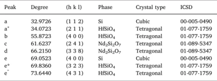
The samples described above were characterized by the XRD method. XRD patterns recorded with the symmetric geometry are shown in Fig. 3a, b. The both types of studied films in as-deposited states demonstrate a series of XRD peaks that can be attributed to the different phases. The very intensive two XRD peaks at 32.9726° (Figs. 3b) and 69.0523° (Fig. 3a and b) were identified as the XRD
signal of the Si substrates, i.e. from (112) and (400) planes in cubic Si crystal lattice (Table 1). Additionally, a set of XRD peaks with the low intensity (Table 1) was assigned to the X-ray diffraction in the
tetra-gonal Nd2Si2O7and tetragonal HfSiO4phases (Table 1). These phases
were supposed to be appeared in thefilm due to the high deposition temperature of 400 °C.
The thermal treatment of the Si-HfO2:Ndfilm at TA= 950 °C leads
to the significant changes of XRD patterns. The signal from the tetra-gonal Nd2Si2O7and tetragonal HfSiO4phases disappeared, while the
XRD peaks related to the tetragonal HfO2 phase become significant
(Fig. 3a,Table 2). The intensities offive XRD peaks related to this phase (Fig. 3a, the peaks denoted as 1, 2, 3, 4, 6) increased significantly (Fig. 3a). Additionally, the XRD signal of the cubic Si phase (peak 5) and new XRD peaks, identified as the X-ray diffraction from the crystal planes in the hexagonal Nd2O3(peak 1c) and tetragonal SiO2(peak 1b)
lattices, were detected (Fig. 3a,Table 2). Simultaneously, the improved crystallinity of the Si-HfO2:Ndfilm annealed at TA= 950 °C hampers
the detection of XRD peaks from underlying Si substrate (Fig. 3a). Thermal annealing the Si-N-HfO2:Nd films is less effective. The
crystallization process in thesefilms at TA= 950 °C is completely
dif-ferent (Fig. 3b). All XRD peaks, which were revealed in the as-deposited Si-N-HfO2:Ndfilm, have been detected also after their annealing at
Fig. 3. XRD spectra for Si-HfO2: Nd (a) and Si-N-HfO2: Nd (b)films, as-deposited and annealed at 950 °C. Table 1
XRD peaks in as-deposited Si-HfO2:Nd and Si-N-HfO2:Ndfilms.
Peak Degree (h k l) Phase Crystal type ICSD
a 32.9726 (1 1 2) Si Cubic 00-005-0490 a∗ 34.0723 (2 1 1) HfSiO4 Tetragonal 01-077-1759 b 55.8723 (4 0 0) HfSiO4 Tetragonal 01-077-1759 c 61.6237 (2 4 1) Nd2Si2O7 Tetragonal 01-089-5347 d 66.2150 (3 3 8) Nd2Si2O7 Tetragonal 01-089-5347 e 69.0523 (4 0 0) Si Cubic 00-005-0490 e* 69.8360 (3 2 3) HfSiO4 Tetragonal 01-077-1759 e” 73.6440 (4 3 1) HfSiO4 Tetragonal 01-077-1759 Table 2
XRD peaks of Si-HfO2:Ndfilm annealed at 950 °C (Fig.3a).
Peak Degree (h k l) Phase Crystal type ICSD
1a 30.0643 (1 0 1) HfO2 Tetragonal 00-008-0342 1b 30.1870 (1 1 0) SiO2 Tetragonal 00-045-1374 1c 30.7750 (1 0 1) Nd2O3 Hexagonal 00-041-1089 2a 34.1623 (0 0 2) HfO2 Tetragonal 00-008-0342 2b 35.1123 (2 0 0) HfO2 Tetragonal 00-008-0342 3a 49.9123 (2 0 2) HfO2 Tetragonal 00-008-0342 3b 50.2723 (2 2 0) HfO2 Tetragonal 00-008-0342 4a 59.7523 (3 1 1) HfO2 Tetragonal 00-008-0342 4b 59.9723 (2 2 2) HfO2 Tetragona 00-008-0342 4c 60.4242 (1 2 1) SiO2 Tetragonal 00-045-1374 5 69.0523 (4 0 0) Si Cubic 00-005-0490 6 82.1823 (2 0 4) HfO2 Tetragonal 00-008-0342
950 °C (Fig. 3b). Additionally, the new XRD peaks (Fig. 3b, peaks 1–6) have appeared and were attributed to the tetragonal HfSiO4 phase
(Table 3). Note that owing to the less effective crystallization process in
the Si-N-HfO2:Ndfilm at 950 °C, the peaks related to the XRD in the Si
substrate can be still detected in the XRD pattern (Fig. 3b).
3.4. Light-emitting properties
The luminescent spectroscopy is a powerful tool for the character-ization of rare-earth doped materials. Hereafter the most interesting results for thefilms described above will be presented. Note that the majority researchers were focused early on the investigation of the near-infrared PL spectrum in the range 800–1400 nm [10–16]. Typical radiative emission bands of Nd3+ions in the mentioned range can be
detected at 880, 1060, and 1350 nm [10,22–24]. These emission bands originate from the electronic transitions between 4fN levels:4F3∕2→ 4I
9∕2,4F3∕2→4I11∕2and4F3∕2→4I13∕2in Nd3+ions (Table 4).
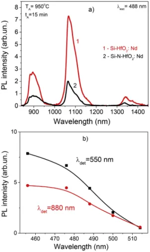
It is essential that the high PL intensity in the studiedfilms was detected for the annealedfilms. The spectra registered in the visible and IR spectral ranges with the excitation by the 325 nm line of a He-Cd laser and 488 nm line of an Ar+-ion lasers are shown inFig. 4and
Fig. 5a, respectively. The total PL intensity has non-monotonic behavior with annealing temperature. The highest PL intensity was detected for the films annealed at TA= 900–950 °C whatever the deposition
ap-proaches.
Fig. 4a shows the visible PL spectra of the Si-HfO2:Ndfilms in the
as-deposited state and after annealing at TA= 950 °C. As one can see, the
PL spectrum consists the several PL components related to the optical transitions in the 4f inner electronic shell of Nd3+ions with a set of peaks in the spectral range of 350–900 nm (Table 4). Their contribution depends on the annealing temperature and governs the shape of total PL spectrum. The crystallization of the Si-HfO2:Ndfilm upon annealing at
950 °C and the appearance of the tetragonal HfO2 crystal phase
(Table 2) lead to significant increasing the PL intensity of visible and IR
PL bands (Table 4,Fig. 6).
In contrary, the PL spectra of the Si-N-HfO2:Ndfilm are still
fea-tureless after annealing at TA= 950 °C (Fig. 4b). Actually, the PL
in-tensity increases after annealing, but whatever the annealing tem-peratures, PL spectra demonstrate broad unstructured PL bands with the main peak within 440–480 nm and other small PL peaks in the range of 750–900 nm (Fig. 4b). Thus the less effective crystallization of
the Si-N-HfO2:Ndfilm upon annealing (Fig. 3b) no permit re-arranging
the Nd3+ions in host matrix that is necessary to obtain the efficient
radiative defects.
Fig. 5a represents the PL spectra of both films in the range of 800–1400 nm. One can see that the typical radiative emission bands of Nd3+ions are detected at 880, 1060, and 1350 nm. The spectra have similar shape. The difference in the intensity can be explain by the less effective crystallization of the Si-N-HfO2:Nd film upon annealing and lower amount of the sensitizers in Si-N-HfO2:Nd that can excite the
Nd3+ions. Another reason can be the competition between different radiative channels contributed in the visible broad PL band.
The effect of the excitation wavelengths on the intensity of PL bands centered at 550 nm and 880 nm is shown inFig. 5b for the Si-HfO2:Nd
film. As one can see, the PL bands at 550 nm and 880 nm have the similar PL intensities under the excitation with the 500 nm and 514 nm light wavelengths. However, at shorter excitation wavelengths, the 880-nm Nd3+PL band demonstrates some kind of saturation, whereas the
550-nm PL bands increases in the intensity. It is worth to point that 476 and 455 nm excitation is the non-resonant and resonant excitations for the Nd3+ions, respectively (Table 4). The similar intensities of the
880-nm Nd3+PL band related to the4F
3/2→4IJ(J = 9/2) radiative
transi-tion detected at the both excitatransi-tions (resonant and non-resonant) give the evidence that the rare-earth ions are excited via energy transfer from the Si nanoclusters or host defects as well. Recently we have de-monstrated such effect for the Er-doped and Pr-doped HfSiO films [8,9]. The increase of annealing temperatures results in decreasing the PL intensity of Nd-related PL bands in the both types of investigatedfilms. This can be due to the formation of Nd-oxide or Si-oxide phases, as well as due to decreasing the number of sensitizers, for instance, the Si
Table 3
XRD peaks of Si-N-HfO2:Ndfilm annealed at 950 °C (Fig.3b).
Peak Degree (h k l) Phase Crystal type ICSD
a 33.0126 (1 1 2) Si Cubic 00-005-0490 a∗ 34.0723 (2 1 1) HfSiO4 Tetragonal 01-077-1759 1 38.6826 (2 2 0) HfSiO4 Tetragonal 01-077-1759 2 40.7726 (2 0 2) HfSiO4 Tetragonal 01-077-1759 3 44.0526 (3 0 1) HfSiO4 Tetragonal 01-077-1759 c 61.6237 (2 4 1) Nd2Si2O7 Tetragonal 01-089-5347 4 64.6307 (4 0 2) HfSiO4 Tetragonal 01-077-1759 d 66.2150 (3 3 8) Nd2Si2O7 Tetragonal 01-089-5347 e 69.0523 (4 0 0) Si Cubic 00-005-0490 e* e∗ 69.8360 73.6440 (3 2 3) HfSiO4 Tetragonal 01-077-1759 (4 3 1) HfSiO4 Tetragonal 01-077-1759 5 76.4726 (4 1 3) HfSiO4 Tetragonal 01-077-1759 __6__ 81.1056_ (5 1 2] HfSiO4 Tetragonal 01-077-1759 Table 4
Optical transitions detected in Si-HfO2:Ndfilms (Fig. 4a).
Number Wavelength, nm Optical transition Reference
1 400 4P 1/2→4I9∕2 [14] 2 455 4G 11/2→4I9∕2 [=23,24] 3 540–550 4G 7/2→4I9∕2 [12,24] 4 560 4G 5/2→4I9∕2 [12,22] 5 660 4F 9∕2→4I9∕2 [10] 5 650 2G 7/2→4I9∕2 [24] 6 710 4F 7∕2→4I9∕2 [24] 7 790 2H 9/2,4F5∕2→4I9∕2 [22] 8 880 4F 3∕2→4I9∕2 [10] 9 1074 4F 3∕2→4I11∕2 [10] 10 1330 4F 3∕2→4I13∕2 [10]
Fig. 4. PL spectra for Si-HfO2: Nd (a) and Si-N-HfO2: Nd (b)films, as-deposited and annealed at 950 °C, detected by a photo multiplayer tube.
nanoclusters, caused by their oxidation, or recovering the host defects. 4. Conclusions
In the present work, the effects of deposition and annealing condi-tions on the emission, chemical composition and structural properties of the Si-HfO2:Nd and Si-N-HfO2:Ndfilms have been studied. The
Nd-related emission was achieved via the direct excitation of the ions as well as by the excitation via Si-nanoclusters. It is also demonstrated that in the film grown in pure argon plasma, the formation of the nano-crystal tetragonal HfO2phase upon high-temperature annealing favors
the bright emission related to the optical transitions via the 4f inner electronic levels in Nd3+ions. Using the argon-nitrogen plasma allows the fabrication of films with the same composition, but the smooth surface that may be interesting for optic waveguide applications. The annealing of these films is less efficient in terms of the film crystal-lization. It was shown that the highest Nd-related PL emission can be obtained from thefilms heat treated at 900–950 °C.
Acknowledgements
This work was partly supported by National Academy of Sciences of Ukraine (project III-4-16), Ministry of Education and Science (project ID: 89452), the French National Agency of Research (ANR), as well as by the CONACYT Mexico (project 258224) and SIP, IPN Mexico (project 20180495).
References
[1] M. Park, T. Schenk, C.M. Fancher, E.D. Grimley, C. Zhou, C. Richter, L.M. LeBeau, J.L. Jones, T. Mikolajick, U. Schroder, J. Mater. Chem. C 5 (2017) 4677. [2] S. Starschich, T. Schenk, U. Schroder, U. Boettger, Appl. Phys. Lett. 110 (2017)
182905.
[3] M.H. Park, T. Schenk, M. Hoffmann, S. Knebel, J. Gartner, T. Mikolajick, U. Schroder, Nanomater. Energy 36 (2017) 381.
[4] L.X. Liu, Z.W. Ma, Y.Z. Xie, Y.R. Su, H.T. Zhao, M. Zhou, J.Y. Zhou, J. Li, E.Q. Xie, J. Appl. Phys. 107 (2010) 024309.
[5] G.C. Righini, S. Berneschi, G. Nunzi Conti, S. Pelli, E. Moser, R. Retoux, P. Féron, R.R. Gonçalves, G. Speranza, Y. Jestin, M. Ferrari, A. Chiasera, A. Chiappini, C. Armellini, J. Non-Cryst. Sol. 355 (2009) 1853–1860.
[6] N.D. Afify, G. Dalba, F. Rocca, J. Phys. D Appl. Phys. 42 (2009) 115416. [7] L. Minati, G. Speranza, V. Micheli, M. Ferrari, Y. Jestin, J. Phys. D Appl. Phys. 42
(2009) 015408.
[8] L. Khomenkova, Y.-T. An, D. Khomenkov, X. Portier, C. Labbé, F. Gourbilleau, Phys. B Condens. Matter 453 (2014) 100–106.
[9] R. Demoulin, G. Beainy, C. Castro, P. Pareige, L. Khomenkova, C. Labbé, F. Gourbilleau, E. Talbot, Nano Futures 2 (2018) 035005.
[10] V. Monteseguro, M. Rathaiah, K. Linganna, A.D. Lozano-Gorrín, M.A. Hernández-Rodríguez, I.R. Martín, P. Babu, U.R. Rodríguez-Mendoza, F.J. Manjón, A. Muñoz, C.K. Jayasankar, V. Venkatramu, V. Lavín, Opt. Mater. Express 5 (2015) 1661. [11] M. Pollnau, P.J. Hardman, W.A. Clarkson, D.C. Hanna, Optic Commun. 147 (1998)
203.
[12] E.O. Serqueira, N.O. Dantas, Optic Lett. 39 (2014) 131.
[13] G. Yi, W. Li, J. Song, B. Mei, Z. Zhou, L. Su, J. Eur. Ceram. Soc. 38 (2018) 3240. [14] M. Balestrieri, S. Colis, M. Gallart, G. Ferblantier, D. Muller, P. Gilliot,
P. Bazylewski, G.S. Chang, A. Slaouib, A. Dinia, J. Mater. Chem. C 2 (2014) 9182. [15] C.-H. Liang, O. Debieu, Y.-T. An, L. Khomenkova, J. Cardin, F. Gourbilleau, J.
Lumin. 132 (2012) 3118.
[16] P. Pirasteh, J. Charrier, Y. Dumeige, J.-L. Doualan, P. Camy, O. Debieu, Ch-H. Liang, L. Khomenkova, J. Lemaitre, Y.G. Boucher, F. Gourbilleau, J. Appl. Phys. 114 (2013) 014906.
[17] L. Miotti, K.P. Bastos, G.V. Soar, C. Driemeier, R.P. Pezzi, J. Morais, I.J.R. Baumvol, A.L.P. Rotondaro, M.R. Visokay, J.J. Chambers, M. Quevedo-Lopez, L. Appl. Phys. Lett. 85 (2004) 4460.
[18] B.A. Movchan, A.V. Demchishin, Fiz. Metal. Metalloved. 28 (1969) 653. [19] J.A. Thornton, J. Vac. Sci. Technol. 11 (1974) 666.
[20] P.B. Barna, A. Adamik, Thin Solid Films 317 (1998) 27. [21] S.-S. Lin, C.-K. Peng, C.-W. Li, J. Alloy. Comp. 770 (2019) 433.
[22] J. Cui, G.A. Hope, Raman andfluorescence spectroscopy of CeO2, Er2O3, Nd2O3,
Tm2O3, Yb2O3, La2O3, and Tb4O7, J. Spectroscopy (2015) 8 V. 2015, ID 940172
https://doi.org/10.1155/2015/940172.
[23] L. Liu, M. Li, Sh Cai, Y. Yang, Y. Mai, Opt. Mater. Express 5 (2015) 756. [24] T. Som, B. Karmakar, J. Alloy. Comp. 476 (2009) 383.
Fig. 5. a) PL spectrum of the Si-HfO2: Nd (1) and Si-N-HfO2:Nd (2)films an-nealed at 950 °C in the range 850–1500 nm. The spectra are normalized for the film thickness. The excitation wavelength is 488 nm (non-resonant for Nd3+ ions). b) Variation of PL intensity for the PL peaks at 550 nm and 880 nm versus excitation wavelength detected in the Si-HfO2: Ndfilm annealed at 950 °C.
Fig. 6. Excitation and recombination optical transitions via the 4f inner elec-tronic levels detected for the Nd3+ions embedded in Si-HfO
2:Ndfilms. The Nd3+energy level diagram was taken from Ref. [11].