HAL Id: hal-01453463
https://hal.archives-ouvertes.fr/hal-01453463
Submitted on 3 Mar 2017
HAL is a multi-disciplinary open access archive for the deposit and dissemination of sci-entific research documents, whether they are pub-lished or not. The documents may come from teaching and research institutions in France or abroad, or from public or private research centers.
L’archive ouverte pluridisciplinaire HAL, est destinée au dépôt et à la diffusion de documents scientifiques de niveau recherche, publiés ou non, émanant des établissements d’enseignement et de recherche français ou étrangers, des laboratoires publics ou privés.
Structural and emission properties of Tb3+-doped
nitrogen-rich silicon oxynitride films
Christophe Labbe, Yong-Tao An, Grzegorz Zatryb, Xavier Portier, Artur
Podhorodecki, Philippe Marie, Cedric Frilay, Julien Cardin, Fabrice
Gourbilleau
To cite this version:
Christophe Labbe, Yong-Tao An, Grzegorz Zatryb, Xavier Portier, Artur Podhorodecki, et al.. Struc-tural and emission properties of Tb3+-doped nitrogen-rich silicon oxynitride films. Nanotechnology, Institute of Physics, 2017, �10.1088/1361-6528/aa5ca0�. �hal-01453463�
1
Structural and emission properties of Tb
3+-doped nitrogen-rich
silicon oxynitride films
C. Labbé,1 Y.-T. An,1 G. Zatryb,2 X. Portier,1 A. Podhorodecki, 2 P. Marie 1, C. Frilay 1, J. Cardin
1
and F. Gourbilleau1
1
CIMAP CIMAP, Normandie Univ, ENSICAEN, UNICAEN, CEA, CNRS, 6 Boulevard Maréchal Juin 14050 Caen Cedex 4, France2Department of Experimental Physics, Wroclaw University of Technology, 50-370 Wroclaw, Poland
E-mail: christophe.labbe@ensicaen.fr
Received 1 June 2016, revised 8 October 2016 Accepted for publication 30 November 2016 Published 17 February 2017
Abstract
Terbium doped silicon oxynitride host matrix is suitable for various applications such as light emitter compatible with CMOS technology or frequency converter system for photovoltaic cells. In this paper, amorphous Tb3+ ions doped nitrogen rich silicon oxynitride (NRSON) thin films were fabricated by reactive magnetron co-sputtering method, using various N2 flows and
annealing conditions, in order to study their structural and emission properties.
The Rutherford Backscattering Scattering (RBS) measurements and the refractive index values, confirmed the silicon oxynitride nature of the films. An electron microscopy analysis conducted for different annealing temperatures (TA) was also performed up to 1200 °C. The Transmission
Electron Microscopy (TEM) images revealed two different sublayers. The top layer showed porosities coming from a degassing of the oxygen element during the deposition and the annealing, while in the region close to the substrate, a multilayer-like structure of SiO2 and Si3N4
phases appeared, involving a spinodal decomposition. Upon a 1200 °C annealing treatment, an important density of Tb clusters was detected, indicating a higher thermal threshold of rare earth (RE) clusterization in comparison to the silicon oxide matrix.
With an opposite variation of the N2 flow during the deposition, the nitrogen excess parameter
2
Infrared (FTIR) spectra behavior and the emission properties. Different vibration modes of the Si-N and Si-O bonds have been carefully identified from the FTIR spectra, characterizing such host matrix, especially the "out-of-phase" stretching vibration mode of the Si-O bond.
The highest Tb3+ photoluminescence (PL) intensity was obtained by optimizing the N incorporation and the annealing conditions. In addition, according to these conditions, the integrated PL intensity variation confirmed that the silicon nitride-based host matrix had a higher thermal threshold of rare earth clusterization than its silicon oxide counterpart. The analysis of time-resolved PL versus TA, showed the impact of the Tb clustering on the decay times, in
agreement with the TEM observations. Finally, the PL and PL excitation (PLE) experiments and comparison of the related spectra between undoped and Tb-doped samples were carried out to investigate the impact of the band tails on the excitation mechanism of Tb3+ ions.
1. Introduction
The Tb3+ ions are attractive energy acceptors for silicon photonics applications due to their important emission lines at blue and green colors ascribed to its 5D3 and 5D4 energy levels.
Consequently, Tb3+ ions doped silicon oxide films have been investigated as a promising luminescent material compatible with CMOS technology. If we restrict the deposition techniques used to form such a rare earth (RE) doped thin films to implantation, Molecular Beam Epitaxy (MBE), magnetron sputtering and Plasma-Enhanced Chemical Vapor Deposition (PECVD), the most common host matrix for the Tb3+ ions is SiO2 [1-4]. Some works in the literature reached a
step forward by fabricating various devices based on this matrix [4-7]. Some investigations have also been carried out on Tb3+: SiC(N) materials [8-10] as well as on the silicon rich silicon oxide films (Tb3+:SRSO)[11] with CMOS devices [12]. However, the incorporation of silicon excess in SRSO, contributing to the formation of Si nanoclusters, significantly reduced the emission intensity of lanthanide ions as a result of a strong non-radiative recombination [13-15].
For this reason, some researchers have focused their works on silicon (oxy)nitride thin films with the aim to find efficient light sources directly integrated on optical chips [16]. Indeed, the silicon oxynitride host is an attractive choice, because of its relatively small band gap (4~5 eV) which may play an important role in the energy transfer from matrix to RE ions with an efficient
3
electrical injection [17]. Moreover, this matrix should have much higher RE ions solubility in comparison to its silicon oxide counterpart and then allow to prevent RE clustering ions [18]. Furthermore, Si rich silicon nitride (SRSN) has been investigated since Si excess can form clusters which act as luminescence centers to enhance RE emission [19]. In contrast to this, various studies mention the role played by the localized states in the band tails of the amorphous matrix acting as sensitizers for RE emission [16, 20-22]. As underlined by Yerci et al., the addition of N atoms introduces more disorder than in the case of SRSO matrix[16]. In this case, by contrast with the Si excess, the N excess (Nex) would introduce many defects leading to the
appearance of band tails. For this reason, one can expect an efficient sensitization of RE ions in nitrogen rich silicon (oxy)nitride (NRS(O)N) films [17, 23].Indeed, for such matrices an intense Tb3+ photoluminescence (PL) signal was observed by Jeong et al. [24], Yuan et al. [25] and by our group [26], even for non-resonant excitation. From these results, two significant applications have been demonstrated using a Si-based host matrix: a CMOS device based on a Tb3+:SiOxNy/SiO2 superlattice [27] and a photovoltaic application based on a down converter
system [28, 29]. Therefore, the Tb3+ excitation mechanism in NRSON requires further investigations in order to fully understand this key mechanism for applications.
In this study, we investigate the structural and optical properties of Tb-doped NRSON films. These films were fabricated by reactive magnetron co-sputtering method for different reactive nitrogen flow and the annealing temperature (TA). Rutherford Backscattering Scattering (RBS),
Transmission Electron microscopy (TEM) as well as Energy-Filtered TEM (EFTEM) measurements have been performed to analyze the composition and structure of these samples. An investigation of different vibration modes of the Si-N and Si-O bonds was conducted using Fourier Transform Infrared (FTIR) spectrometer. Taking into account both the reactive flux and the annealing effect, we reported here the optimal conditions for preparation of highly luminescent samples and discussed the Tb-clusterization effect. Finally, the energy transfer mechanisms between the NRSON host matrix and the Tb3+ ions were considered.
2. Experimental details
In this work, Tb-doped NRSON films were deposited onto p-type 250 μm-thick (100)-oriented Si wafers by reactive radio frequency magnetron co-sputtering of a pure Si target topped with 5
4
Tb4O7 pellets under pure nitrogen plasma. The N gas flux was varied from 3 to 9 sccm, while the
plasma total pressure was concomitantly changed in the range of 4-28 µbar. The deposition temperature (Td) and RF power density were fixed at 200°C and 1.23 W.cm-2, respectively. The
annealing was processed under a given N flow, at temperatures (TA) varying from 500 °C to
1200 °C during 1 hour.
The chemical composition of the layers was obtained by RBS measurements using a 1.5 MeV
4
He+ ion beam with a normal incidence and a scattering angle of 165 °, revealing the relative atomic concentrations (% at.) of the different elements. TEM was used to observe the evolution of the structure of the samples upon annealing. For such observations, cross sectional thin foils were prepared by means of a FEI HELIOS Nanolab 660 focused ion beam until electron transparency. The samples were then investigated using a double corrected JEOL ARM200 operated at 200 keV, equipped with a cold field emission gun, and a GATAN imaging filter (GIF) (QUANTUM 965ER spectrometer). The chemical analyses were performed by EFTEM using the image mode of the GIF to analyze the composition variation of the layers. The digitized images were processed by the commercial GATAN software called DIGITAL-MICROGRAPH. The microscope is also equipped with an Energy Dispersive X-Ray (EDX) spectrometer for chemical analyses.
The FTIR spectra were recorded in the range of 500-4000 cm-1 using a Nicolet Nexus spectrometer under normal and Brewster's incidence (65 °) angles. The optical properties of the layers have been characterized using Ellipsometry and Photoluminescence spectroscopy measurements. For the former, they were conducted by means of UVISEL Jobin-Yvon ellipsometer with an incident angle of 66.2 °. The experimental spectra were recorded on a 1.5–5 eV range with a 0.01eV resolution. The refractive indexes, given at 1.95 eV, as well as the thicknesses, were deduced from the experimental data by a dispersion law derived from the Forouhi–Bloomer model for amorphous semiconductors using the DeltaPsi2 software [30]. The thickness and refractive index uncertainties are ±10 nm and ±0.01 respectively. Finally, photoluminescence (PL) and PL excitation (PLE) spectra were performed at room temperature by means of a Jobin-Yvon Fluorolog spectrophotometer using a 450W Xe lamp as excitation source with a spectral resolution lower than 5 nm. The PL lifetime was obtained by means of an optical parametric oscillator with a 5 ns pulse at full width at half maximum and a 10 Hz repetition rate
5
for a 244 nm wavelength excitation. The spot diameter was 500 µm with an average energy of 15 mJ.
3. Elemental composition analysis
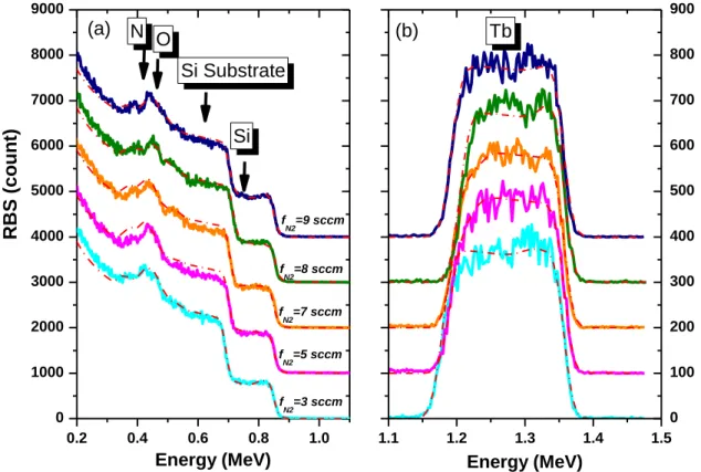
Elemental compositions of the as-deposited (AD) samples were determined by RBS measurements. Figure 1(a) shows RBS spectra ranging from 0.20 up to 1.10 keV for the samples obtained with different N flows. The backscattering signals from N and O atoms can be seen in figure 1(a), along with the Si one coming from both thin film and substrate as reported in previous works [14, 27]. Note that the oxygen content in the films is originating from the Tb4O7
chips. The slight change in the curve shape indicates a small variation of the composition of these films (Figure 1(a)). Figure 1(b) shows RBS spectra in the 1.15 up to 1.40 keV range, which corresponds to the backscattering from Tb3+ ions. The width of the Tb-related band changes from sample to sample due to their different thicknesses (230-280 nm), coming from the different N gas flux. The band intensities (RBS yields) are very similar indicating that the Tb content is almost the same for all the films. Moreover, Tb spatial distribution in each sample is quite uniform across the film thickness.
6
Figure 1. RBS experimental spectra of the AD samples with the corresponding N flow. Si, O and N elements are displayed on the left side (a), whereas the RBS spectra of Tb atoms are shown on the right (b). A simulated curve using SIMNRA software is added to each experimental RBS spectrum (red curves). The spectra have been arbitrarily up-shifted for clarity.
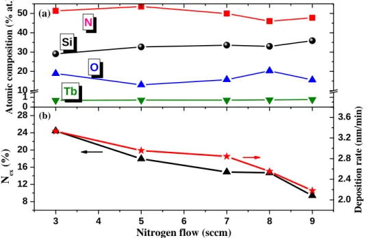
By fitting RBS spectra as shown in figure 1, the film compositions were obtained (see figure 2(a)). The fits require the use of two layers: one at the top of the film (so called "top layer") in contact with air and another one at the interface near the substrate (so called "interface layer"). The ratio between the resulting top and interface layer's thicknesses varied from three (190 nm/60 nm) to one third (60 nm/190 nm). Atomic concentrations are calculated considering the weight of the interface and top layers thicknesses. As can be seen in figure 2(a), the Tb concentration is constant in all of the investigated films and equal to 0.730.05 at.%. The fact that Tb has a homogenous distribution within the whole film for the AD samples differs from Tb-doped SRSO layers. Indeed, for SRSO host matrix, it has been shown that Tb ions tend to agglomerate and form clusters close to the film/substrate and film/air interfaces, even for low concentration (0.1 at.%.) [14]. As expected, the nitride matrix seems to prevent such an agglomeration process even for 7 times higher Tb concentrations. This issue is discussed further in another section (§7).
0.2 0.4 0.6 0.8 1.0 0 1000 2000 3000 4000 5000 6000 7000 8000 9000 f N2=5 sccm N f N2=7 sccm f N2=9 sccm f N2=3 sccm f N2=8 sccm Si O R B S (c o u n t) Energy (MeV) Si Substrate (a) 1.1 1.2 1.3 1.4 1.5 0 100 200 300 400 500 600 700 800 900 (b) Energy (MeV) Tb
7
Regarding the other elements, the O content varies between 13 at.%, and 17 at.%, while the Si content increases from 29 at.% up to 36 at.%. Surprisingly, a slight decrease of the N concentration of almost 5 at.% is observed with increasing the N flow.
Figure 2. (a) Atomic compositions of the Tb-doped NRSON films as a function of N2 flow (b) Nex (left scale) and
deposition rate (right scale) versus N2 flow for AD layers.
To push further investigation, N excess (Nex) has been deduced using the following relation:
𝑁𝑒𝑥(%) = ([𝑁] − 43[𝑆𝑖] + 2
3 [𝑂] −76 [𝑇𝑏]
[𝑁] + [𝑂] + [𝑆𝑖] + [𝑇𝑏] ) × 100
where the term [element] represents the atomic concentration (at.%) of the element (see supplementary data). This ratio gives the deviation from a perfect SiO2 and Si3N4 mixture [28, 31]
and highlights the N importance compared to the other elements. The N excess evolution as a function of N flow is displayed in figure 2(b). Clearly, Nex decreases with N flow, having values
from 24.4 %, 17.9 %, 14.9 %, 14.7 %, to 9.4 % (see the left scale of figure 2(b)) which corresponds to the samples called S24, S18, S15, S14, and S9, respectively. Such a behavior seems to
be linked with the layer deposition rate (right scale of figure 2(b)), which gradually decreases when the N2 flow increases. Similar result has been obtained by Xu et al. [32], who suggested
0 1 10 20 30 40 50 (a) A to mi c co mpo si ti o n ( % a t. ) N Si O Tb 3 4 5 6 7 8 9 8 12 16 20 24 28 (b) N ex (%) Nitrogen flow (sccm) 2.0 2.4 2.8 3.2 3.6 D epo si ti o n ra te ( n m/ mi n )
8
that, from target to substrate, the ejected species collide and/or react with N2 leading to the
modification of the mean free path. Thus, some species do not have enough energy to reach the substrate. Consequently, one can assume that a high N2 flow is unfavorable to the incorporation
of N atoms and to the deposition rate of the growing film.
4. Refractive index analysis
The refractive index was also investigated. The bilayer model used to estimate the refractive index by fitting with DeltaPsi software is consistent with the bilayer model used in RBS analysis. The refractive index increases from 1.54 up to 1.79 with N content. These low index values are between those of the stoichiometric Si3N4 (n=2.04) and SiO2 (n=1.45) materials, confirming that
we have fabricated an oxynitride matrix [17, 33, 34].
5. Microscopic analysis of the annealing temperature effect
In this section, we present different TEM images of the S9 sample in a cross-section configuration
for different TA values. These images were obtained for AD sample and for samples annealed at
9
Figure 3: Cross-sectional TEM images for AD (a) and 700°C annealed S9 samples (b). Some vertical porosities
are clearly observed in the enlarged images in both cases.
According to these observations, the deposited thin films remain amorphous (no diffracting particles) whatever the post annealing treatment applied. The AD S9 sample presents porosities
coming from almost the middle of the film (dashed horizontal line in figure 3(a)) and form vertical tortuous columns of nanoscale diameters in the direction of the top surface (figure 3(a), zoom inset) using a slight defocus condition. These hollow columns are more visible upon 700 °C annealing (figure 3(b), zoom inset) which is probably related to the degassing of light elements from the film (O and/or N) during annealing. But the deposition process itself, occurring almost for two hours at a substrate temperature of 200 °C, seems to have the same effect since similar microstructure is observed for the AD sample. Apparently, this degassing process coming from almost the middle of the film, results in a two layers structure. These results confirm our previous assumption with two modeled layers, named top and interface layers, used for the RBS and the refractive index modeling. Note that this limit between these layers can change without apparent logic between one quarter to three-quarters of the full thickness. The same kind of degassing has been also confirmed by TEM observations on other samples (not shown here). 1 0 0 n m 1 0 0 n m Porosities Porosities Si Substrate Si Substrate As-deposited
a)
TA=700 °Cb)
Interface layer Top layer10
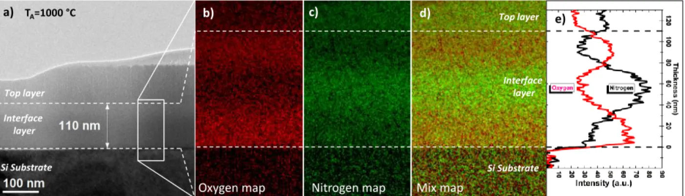
Figure 4. 1000 °C annealed S9 sample investigated through: (a) a cross-sectional bright field TEM image, the
corresponding elemental EFTEM maps of (b) oxygen in red color, (c) nitrogen in green color, (d) mix map and (e) chemical profiles of the N and O from the region delimited by a white square in the TEM image. The ratio of integrated profiles between N and O amounts corresponds to the ratio of the RBS measurements (34.39 at.% for N and 30.59 at.% for O) inside the interface layer.
To investigate this issue in more detail, the S9 sample has been annealed at higher
temperature (TA=1000 °C) and EFTEM images (figure 4(a)), displaying O and N maps, have
been recorded for the whole thickness of this film, by using their respective K edges at 532 eV and 401 eV. Unfortunately, the rare earth element concentration remains too low to be imaged by this technique. Noteworthy, the silicon profile map (not shown) has a homogenous distribution in the film, by contrast with the O and N profiles shown in figures 4(b)-(e). Indeed, concerning the interface layer, O is highly concentrated both on the top and on the bottom (figure 4(b)), whereas N is concentrated mostly in the middle (figure 4(c)). Surprisingly, the profiles of these two last elements offer a clear complementary contrast, displaying a kind of multilayer structure. Note that such N, O distributions are also noticed for the AD and all the annealed layers.
Concerning the top layer, the EFTEM maps reveal poor O content while the N is homogeneously distributed as we can see in figure 4(e), where only the bottom of the top layer is visible but the whole top layer has a uniform distribution of these elements. The low O content, confirmed by RBS measurements (0.1 at. %), suggests the degassing coming from this element. The oxygen may diffuse towards the surface, symbolized by the boundary between the top and the interface layer (figures 4(a)-(e)), featuring the possible physical limit for a degassing inside a solid phase. This frontier position does not appear to vary significantly with the thermal budget (figures 3(b) and 4(a)), suggesting that this effect appears during the deposition (figure 3(a)).
Oxygen map Nitrogen map
Top layer Si Substrate Interface layer Mix map c) d) b) Interface layer Top layer Si Substrate a) TA=1000 °C e)
11
This limit as well as the separation of the two different elements (figure 4(d)), highlighting an unmixing inside the interface layer, are strictly parallel to the substrate surface. These boundaries could be induced by the stress evolution of the film during the deposition [35]. More precisely, this observation suggests a stress-induced diffusion of N by the Si substrate [36, 37], or at least an evidence of the significant role of this interface, leading to a phase separation with a predominant SiO2 phase when O content is important and a main Si3N4 phase if it is weak.
Then, the film/substrate interface could be at the origin of a surface-directed spinodal decomposition (SDSD)[38] in the pseudobinary (SiO2)x(Si3N4)1-x alloy system. As a matter of
fact, such unintended multilayer structure has already been observed by Lui et al. [39] for (HfO2)x(SiO2)1-x alloy system near the substrate and has been attributed to a spinodal
decomposition (SD) [38]. Another similar effect has been noticed for Si-rich-HfO2 materials, but
in this case, coming from the air-film interface with HfO2 and SiO2 phases [40]. Such a SDSD
process has also been shown in ZrO2-SiO2, La2O3-SiO2 and Y2O3-SiO2 systems [41]. The SD is
also the process at the origin of the formation of Si nanoclusters in SiOx or SiNx host matrices
due to the high Si content [42-44]. In our case, the Nex could be at the origin of such effect
assisted by a stress-induced diffusion. In addition, the deposition occurs at 200 °C which is a relatively high deposition temperature for a magnetron co-sputtering process, providing a degassing affecting also the SDSD. Indeed, usually, such SD effect generates a composition wave which has a 4-5 nm periodicity. In our case, this periodicity is approximately one order magnitude higher (30-40 nm), impacted by the degassing and the deposition of our thicker film (230-280 nm). In other studies with Si excess reported in the literature, one can find again the periodicity on a large thickness of almost 40 nm, similarly to our case [42, 43].
12
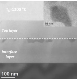
Figure 5. Cross-sectional TEM image of the 1200 °C annealed S9 sample. Tb-rich clusters are visible in the center of
the deposited layer. Inset: zoom of a Tb agglomeration.
A TEM image shown in figure 5 was obtained on the S9 sample annealed at 1200 °C, only to
check the thermal budget threshold at which clusterization occurs. The elemental EFTEM map (not shown) is commented in the supplementary data. The TEM image reveals an important density of clusters with a darker contrast located below the limit between the top/interface layer (dashed line in figure 5), with a size of about 20-40 nm and a lengthening following this boundary. Note that such clusters have started to be detected (weakly contrasted) for samples annealed at 700°C throughout the thickness of the interface layer. These agglomerates at 1200°C were identified by EDX measurements as amorphous Tb-rich clusters (inset of figure 5). Similar particles have already been observed and identified as Tb-oxide clusters (TbO2, Tb2O3) in SiO2
by Nazarov et al.. Their presence are due to a more stable thermodynamic state of this phase and located in the center of the film for a TA at 900°C and at the air/film and film/substrate interfaces
for a higher TA [6]. Due to the fact that our clusters stay amorphous, they should not be in the
same stoichiometry as mentioned above. In contrast to this observation, a Tb-doped silicon-rich silicon oxide with 50 at.% Si, shows a Tb diffusion from the both film interfaces towards the middle of the film, to become uniform across the film depth [13, 14]. In our case, the surprising position of this clusters line is probably due to the separation between the interface and the top layer, offering a stable energy for the formation of Tb clusters. In any cases, such Tb clusters are completely formed at 1200°C confirming that such host nitride-based matrix is less favorable to
13
RE clustering than its silicon oxide counterpart due to a slower diffusion of RE [18, 27, 45, 46]. In others words, the silicon oxynitride matrix have a higher thermal threshold of RE clusterization compared to the silicon oxide matrix.
6. Infrared spectroscopic analyses
6.1. Constant Nitrogen excess
FTIR spectra were performed on as-deposited S9 (Figure 6) and well as on all NRSON samples
(figure 7). The spectra for the S9 sample were measured under a normal incident angle (figure
6(a)) and Brewster angle (figure 6(b)). As it can be seen, a broad band ranging from 650 cm-1 up to 1350 cm-1 with no sharp peaks is appearing.
Figure 6. FTIR spectra recorded at normal (a) and Brewster angle (65 °) (b) for S9 AD film where the film
absorbance has been normalized to its thickness. The Si-O (LO2) at 810 cm-1 and Si-O (TO2) at 820 cm-1 are not
fitted [47]. 0.00 0.01 0.02 0.03 0.04 0.05 0.06 Si-O TO2 Si-O (LO3 ) A b s o rb a n c e (u .a
.) Normal Si-O (TO3 )
=Si-N-Si= (TO) Si-N (TO) Si3N4 (TO) (a) 600 700 800 900 1000 1100 1200 1300 1400 0.00 0.01 0.02 0.03 0.04 0.05 0.06 (b)
Si-O (TO3-LO3) (TO4-LO4) Out-of-phase Brewster A b s o rb a n c e (u .a .) Energy (cm-1) Si-O TO2-LO2
14
To identify the different peaks constituting such a broad band, we have fitted the normal incident angle spectrum with 5 Gaussian peaks (less would not be consistent with the literature cited in table 1), revealing the transversal optical modes (TO) (figure 6(a)). However, the Brewster angle spectrum reveals the longitudinal modes (LO) and therefore an additional 6th peak appears (figure 6(b)). The fits, with three parameters for one Gaussian peak (position, amplitude, FWHM), are performed without any constraint.
The different peak positions are displayed in table 1. Focusing on the Si-O absorption bands, a well-known peak under normal incident angle is observed at 1070 cm-1 and attributed to the TO3 stretching mode, which is also confirmed under Brewster angle at 1076 cm-1 [47-51].
The LO3 mode is present at 1222 cm-1, compared with 1250 cm-1 and 1254 cm-1 in SiO2 matrix
respectively[47, 49] or 1227 cm-1 and 1250 cm-1 in the case of the SiOxNy matrix[48, 52].
An important third peak is visible at 1128 cm-1 under normal incidence which is blue-shifted at 1146 cm-1 under Brewster angle. This peak cannot be ascribed to the TO4 vibration band usually
localized at 1200 cm-1. This is confirmed with the fact that the appearance of the LO4 mode under
Breswter angle involves rather a red-shifted with a peak located at 1160-1170 cm-1 [47, 53]. Such a peak is attributed to an "out-of-phase" stretching vibration mode of the Si-O bond. Indeed, Pai
et al., [50] based on previous results on local density of vibrational states (LDOVS) by Lucovsky et al. [54], underline a weak coupling of Si atom to O one causing this high frequency edge at
1150 cm-1, the same position we noticed. This first result is confirmed by Kirk et al. who did an investigation of the disorder effect on IR absorption spectra in the a-SiO2 host matrix and found
that the interpretation of the IR spectra is somewhat in contradiction with an independent-oscillator model [47]. Indeed, by introducing disorder-induced mechanical coupling between the LO3-TO3 and LO4-TO4, a broad and significant vibration band appears in the range of 1076-1256
cm-1, corresponding approximately to our bandwidth. Note that the amorphous character of our samples permits to detect a low contribution of the LO peaks even under normal incident angle as reported previously [55]. In addition, the blue-shift observed according to the appearance of the LO mode under Brewster angle for our samples, is in agreement with the spectra displayed by Kirk et al. [47]. This important shoulder in the 1100-1250 cm-1 range under Brewster angle is also shown by previous works on silicon oxynitride host matrix deposited by PECVD technique[56-58].
15
The three last vibration bands are positioned at 867 cm-1, 956 cm-1 and 1024 cm-1 under normal angle (or at 869 cm-1, 953 cm-1 and 1029 cm-1 under Brewster angle) (see table 1). These energies correspond approximately to the positions (903 cm-1, 965 cm-1, 1030 cm-1) found by Naiman et al. after a dispersion analysis on (reoxidized) nitrided oxides on silicon [59], as well as the ones proposed by Moreno et al.[60]. The latter found modes peaking at 896 cm-1, 962 cm-1 and 1026 cm-1 after performing modelling of silicon nitride system. But these peak positions are not ascribed to a specific vibration mode. Our first peak at 867 cm-1 is well known and is originating from the Si-N stretching mode [52, 56, 61-64]. The difference between this first peak position at 867 cm-1 and 903 cm-1 (or 896 cm-1) for the other authors, could suggest that we did not take into account the Si-O TO2-LO2 peaks at 810-820 cm-1 (figures 3(a-b)) [47, 48].
As for the two last peaks at 956 cm-1 and 1024 cm-1, their attribution is more complicated. Focusing on the 956 cm-1 peak, this band could be explained by the Si-OH bending mode but our matrix does not contain any hydrogen [65]. Another possibility could be the existence of an asymmetric mode Si-O-Tb bonds. But, as mentioned by Ono et al.[66], the heavier the element that binds with oxygen atom in Si-O is, the lower the vibrational frequency [66]. Then some authors have observed a vibrational frequency at about 900 cm-1 for a Si-O-Pr [66] or, although Nd is heavier than Pr, around 910-950 cm-1 for Si-O-Nd [67]. Yet, Tb atom is much heavier than the Pr or Nd ones and thus, a vibration at 955 cm-1 for this bond could be excluded. Finally, such a peak at 956 cm-1 was found in a 220 nm-thick SiOxNy [68] and more precisely at the interface
layer with the Si substrate whose thickness was about 2 nm on etched nitrided oxide layer [59]. In a detailed study of Ono et al., this peak, positioned exactly at 960 cm-1, has been attributed to the doubly bonded N atoms associated with two Si atoms (≡Si-N-Si≡) with the asymmetric stretching mode [69].
The last peak found at 1024 cm-1 underlined by the dispersion analysis of Naiman et al. is ascribed, in their previous study, to the planar trigonal bonded nitrogen (Si3≡N4) [68].
Nevertheless, some studies assign this peak to a shoulder of the main (Si-N) stretching band at 870 cm-1 [62, 70, 71].
16 5 Peak positions (cm-1) Normal angle (figure 3(a)) 6 Peak positions (cm-1) Brewster angle (figure 3(b)) Bonds attribution
Vibration modes References
867 869 Si-N TO stretching [52, 56, 59-64]
956 953 ≡Si-N-Si≡ TO Asymmetric stretching [60, 69] 1024 1029 Si3≡N4 TO Asymmetric stretching [60, 68, 70]
1070 1076 Si-O TO3 (stretching) [47-51]
1128 1146 Si-O Out-of-phase (coupling TO3
-LO3 and TO4-LO4)
[47, 49, 50] [56-58]
- 1222 Si-O LO3 [47, 48, 52]
Table 1: Peaks positions for normal and Brewster angles with their corresponding bond and vibration modes.
17 6.2. Variable Nitrogen excess
700 800 900 1000 1100 1200 1300 0.0 0.1 0.2 0.3 0.4 0.5 0.6 2100 2200 2300 2400 0.0 0.1 0.2 0.3 S24 Absorbance (a.u.) Wavenumber (cm-1) (a) S 9
Si-O(TO3-LO3) (TO4-LO4)
Out-of-phase S 15 S14 S18 S 9 S 24 (b) Wavenumber (cm-1) Si-NN
Figure 7. FTIR spectra recorded at Brewster angle (65 °) for AD films for different Nex values (a) in the
650-1350 cm-1 range and (b) in 2050-2300 cm-1 range. See also figure 11 in the supplementary data, which describes (a)
the peaks positions, (b) FWHMs (reflecting the disorder) and (c) peak surfaces (number of bonds) coming from the fits analysis of figure 7(a).
The spectra in figure 7(a) show a blue-shift of the maximum intensity of about 60 cm-1 towards 1075 cm-1 with decreasing the N2 flow inside the deposition chamber and so increasing Nex.
However, we note (see figure 11(a) in supplementary data) that during this Nex rise (9.4 % to 24.4
%), the different peaks positions blue-shifted slightly by only 20 cm-1, except for the Si-N (TO) and Si-O (LO3) modes which did not shift at all. Then this refocusing at 1075 cm-1 is not due to a
shift of all the peaks positions. Such a variation in shape is due to the decreasing of the out-of-phase peak intensity (see figure 11(b-c) in supplementary data). This decrease was already seen for AD films upon N incorporation [57] [58], as well as for annealed samples, [56] obtained by PECVD technique.
18
In the last 2050-2300 cm-1 energy range (figure 7(b)), we note an absorption peak centered at 2202 cm-1. Such a peak is originating from Si-H stretching [72] or isocyanate groups (N=C=O) or nitrile (C≡N) stretching bond [73]. But no H or C atoms were detected in our samples. Nevertheless, the intensities of these peaks seem to be sensitive to the Nex increase. Based on the
study of adsorption of N2 which is chemisorbed on Rh/SiO2 sample, an important absorption peak
at around 2200 cm-1 at low temperature is explained by the N≡N bond linked to the Rh ion [74]. Consequently, our peak can be ascribed to the azide N≡N stretching mode [75], which gives a (Si-N≡N) resulting bond centered at 2202 cm-1 depending of the Nex concentration. Such a peak
attests also the N-rich character of our nitride matrix.
7. Emission properties
7.1. Photoluminescence properties
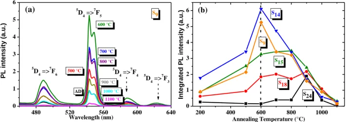
Figures 8(a) to 8(c) show the PL spectra of the samples annealed at different temperatures during one hour in a pure N2 flow. These samples were excited at room temperature using a 325
nm line from a lamp source. This wavelength is non-resonant with energy levels of the Tb3+ ion. As observed, each sample shows four PL peaks centered at about 490, 545, 590, and 624 nm, which correspond to the intra-4f 5D4→7Fj (j = 6, 5, 4, 3) transitions of Tb3+ ions, respectively as
depicted in figure 8(a). These peaks have been already reported in previous studies on Tb:SiN layer obtained by reactive cosputtering [76] or PECVD deposition techniques [24, 25]. For each spectrum, the strongest peak intensity is located at 545 nm (5D4 7F5). This band has been
selected to investigate the TA effect for various Nex. The evolution of its integrated PL intensity
19
Figure 8. (a) PL spectra at 325 nm excitation wavelength of the S9 sample annealed at different TA values during 1h
(b) and the corresponding evolution of integrated PL intensity at 545 nm wavelength versus TA for all the samples.
For all samples, the PL intensity increases with TA, reaches a maximum and starts to decrease for
higher TA values. The former evolution of PL intensity is due to the passivation of non-radiative
channels in the host matrix [77], whereas the latter could be assigned to the combination of two effects. Even if the porosities appear already in the AD sample (Figure 3(a)), the drop of the PL intensity could originate from the rising number of the porosities with annealing, offering more surface recombination centers and providing new non-radiative channels[78]. The second possible effect, which seems to be dominant, is the formation of Tb clusters, such as those observed in the TEM image in figure 5 at TA=1200 °C and already detected at TA=700 °C. These
clusters have a detrimental effect on the PL intensity by the reduction of the number of optically active Tb3+ ions [79]. Such effect is commonly seen for different rare earth-doped Si-based matrix as Nd:SiNx [80] or Er:SRSO [36].
It is interesting to note that the maximum PL intensity appears at different TA values
depending on the Nex. This optimum is reached at TA=600 °C for samples S9 and S14 having both
the lower Nex content (9.4 % and 14.7 %), while it appears at 800 °C for sample S15 and 900 °C
for samples S18 and S24 containing more Nex. The temperatures corresponding to these maxima
seem to be the limiting temperatures below which the cluster formation is not the predominant effect. Above this limit, the RE aggregates are driving down the PL intensity. Apparently, by introduction of a high N excess, the formation of clusters is delayed. This shift of the TA by
almost 300 °C has already been observed for Er ions incorporated either in SiO2 or SiNx [81]. In
480 520 560 600 640 0 1 2 3 4 5 6 800 °C 900 °C S9 1100 °C 1000 °C 700 °C 600 °C 500 °C AD Integrate d PL inte nsity (a .u.) 5 D4 =>7F3 5 D4 =>7F4 5 D4 =>7F6 Wavelength (nm) PL intens ity (a.u. ) 5 D4 =>7F5 (a) 200 400 600 800 1000 0 1 2 3 4 5 6 (b) S14 S9 S15 S18 Annealing Temperature (°C) S24 340 360 380 400 420 440 460 0.0 0.1 0.2 0.3 PL intens ity (a.u. ) S14 700°C 1100°C 1000°C 600°C AD (d) (c) Wavelength (nm) 500°C Tb3+ 5 D 4 3 4 7 F6 5 624 nm 545 nm 590 nm 490 nm
20
this study, the maximum intensity was underlined at TA=800 °C for the silicate matrix while the
maximum is not achieved for the SiNx matrix with a higher thermal budget. Our results confirm
this point and show that the silicon nitride-based host matrix has a higher thermal threshold of RE clusterization than its silicon oxide counterpart [18].
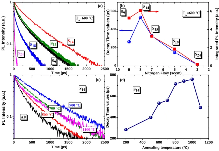
7.2. Time-resolved photoluminescence
Although it is interesting to increase the Nex in the film in order to prevent the formation of Tb
clusters, we have found that the maximum PL intensity is about 3 times lower with a high Nex
value (figure 8(b)). Indeed, such a strongly non-stoichiometric composition may affect the quality of the host matrix and create many non-radiative defects. For deeper investigations, we conducted time-resolved PL measurements. Figure 9(a) displays the PL decays detected at 545 nm (5D4 7
F5) wavelength as a function of Nex, obtained for samples annealed at TA=600 °C. The decay
times deduced from these curves are shown in figure 9(b). Note that the lifetime of band tails-related PL (see §7.3) is usually in the nanoseconds scale which is too short to be measured by our experimental setup [82].
21
Figure 9. At the 545 nm (5D47F5) wavelength (a) the normalized decay curves for samples S9 to S24 annealed at
TA=600 °C and (b) their corresponding decay time with the evolution of the integrated PL intensity (c) the PL decay
curves for the optimized layer S14 annealed at the indicative TA and (d) their corresponding decay time.
The decay curves exhibit a non-exponential behavior and for this reason, we have calculated the mean decay time (𝜏𝑚) using the following equation:
𝜏𝑚 = ∫ (𝐼(𝑡)/𝐼0)𝑑𝑡
∞ 0
where I(t) is a time dependent peak intensity while I0 is the maximum intensity at t = 0s [83]. The
lifetime obtained for the samples annealed at TA=600 °C (figure 9(b)) for the lowest Nex amount
is in the range of several-hundred-μs, comparable to the values reported by other authors [24]. The decay time increases slightly with Nex for S14 sample and then a gradually decrease is noticed
for higher Nex values. The integrated PL intensity displayed in figure 8(b) (dashed line at TA=600
°C) for the same samples, and reported in figure 9(b) (right scale), shows a similar evolution. Therefore, the PL intensity behavior seems to be governed by the non-radiative recombination
0 500 1000 1500 2000 2500 0.1 1 TA=600 °C S24 S14 S18 S15 PL Intens ity (a.u. ) Time (µs) S9 (a) 10 9 8 7 6 5 4 3 2 0 200 400 600 TA=600 °C (b) S24 S18 S15 S14 S9 In te g ra te d P L I n te n s it y ( a .u .) Decay Time v alues (µs ) 0 500 1000 1500 2000 2500 0.1 1 (d) (c) S14 P L I n te n s it y ( a .u .) 700 °C 900 °C 500 °C 1100 °C AD Time (µs) 200 400 600 800 1000 1200 200 400 600 800 S14 D e c a y Ti m e v a lue s ( µ s ) Annealing temperature (°C) 0 2 4 6 Nitrogen Flow (sccm)
22
coming from the increasing population of defects with Nex. This explains why the maximum PL
intensity is about 3 times lower for the highest Nex (figure 8(b)).
To go further in the study of the annealing effect, we present the dependence of the PL decay time of the optimized sample S14 detected at 545 nm with respect to TA (figures 9(c)-(d)). The PL
lifetime increases with TA up to 1000 °C followed by a rapid decrease at 1100 °C. For this later,
as explained above, this can be due to the large number of Tb-rich clusters formed leading to new non-radiative channels. Up to 1000 °C, a reduction of the non-radiative recombination takes place, due to the defects passivation, which causes the increase of the PL lifetime. In that case, one wonders why the PL intensity behavior has a maximum at TA=600 °C (figure 8(b)), while the
lifetime has a maximum shifted for 1000 °C (figure 9(d)). The long average lifetime measured (530 µs at TA=600 °C) comes from the locally isolated Tb3+ ions. The diffusion of Tb3+ ions
probably starts at 600 °C (Tb-rich clusters detected for the 700 °C annealed sample by TEM observations- not shown §5) reducing de facto the number of optically active Tb3+ ions and concomitantly reduces the PL intensity. Consequently, between 600 °C and 1000 °C, the lifetime continues to increase due to the passivation of defects while we observe a reduction of the PL intensity. Such a behavior has been already detected on Er3+ ions in silica glass by Polman et al. [84].
7.3. Excitation mechanisms of Tb3+ ions
Figure 10(a) shows the PL spectra for both undoped and Tb-doped NRSON films annealed at 600 °C during 1h, measured using 380 nm (3.3 eV) excitation line. The undoped sample displays a broad band from about 2.5 to 3.2 eV (500 to 390 nm) originating from the recombination of excitons in band tails (BTs) states [26]. Indeed under such excitation wavelength, the BTs has a significant PL intensity compared to the excitation at 325 nm shown in figure 8(a) and described in our previous study [28]. The Tb-doped sample presents the features of the Tb3+ ion peaks. The overlap between the Tb3+ energy levels and the BTs is evident. This spectral overlap is very important since it allows indirect excitation of Tb3+ ions via BTs states, leading to the observed 5D4→7Fj transitions. The same behavior has already been observed for
undoped [24, 25] and Tb-doped films[24] and is mainly due to the N dangling bond related recombination process.
23
Figure 10. (a) PL spectra of undoped and Tb-doped films annealed at 600 °C during 1h (b) the associated PLE
spectra detected at 390 nm (3.2 eV) related to the BTs (d) 490 nm (2.5 eV) (5D4 → 7F6) and 545 nm (2.3 eV) (5D4 →
7F
5) related to the Tb3+ transitions and (c) the schematic of the Tb3+ energy diagram depicting the energy transfer
between electronic energy levels.
Aiming at understanding the energy transfer mechanism to the Tb3+ ions, PLE experiments were performed for both samples at 3.2 eV (390 nm) detection wavelength related to the BTs PL (Figure 10(b)) and also at 2.5 eV (490 nm) and 2.3 eV (545 nm), corresponding to the 5D4 7F6
and 5D47F5 transitions of the Tb3+ ion (figure 10(d)). In the case of BTs detection, two peaks
appear for the undoped film at 3.3 eV and 4.3 eV (figure 10(b) - black arrows). The first one is identified as a N defect state (N4+) [26], while the second is correlated to the absorption of the
BTs just below the gap [28, 29]. It is linked to the Si–N bonds which introduce localized states due to N-2 lone pair electrons at the top of the valence band[85]. The recombination of holes
1.75 2.00 2.25 2.50 2.75 3.00 3.25 0.0 0.2 0.4 0.6 0.8 1.0 5 D4 =>7F3 5 D4 =>7F4 5 D4 =>7F6 5 D4 =>7F5 (a) PL In te n si ty (a. u .) Tb-doped Undoped exc= 380 nm=3.3 eV (d) 3.5 4.0 4.5 5.0 5.5 0.0 0.2 0.4 0.6 0.8 1.0 (N4+) (BTs) (BTs) det= 390 nm=3.2 eV PL E In te n si ty (a. u .) Wavelength (nm) Undoped Tb-doped Wavelength (nm) (N4+) PL E In te n si ty (a. u .) 3.5 4.0 4.5 5.0 5.5 0.01 0.1 1 (BTs) (b) (c) (N4+) det=545 nm=2.3 eV det= 490 nm=2.5 eV Energy (eV) Energy (eV) Energy (eV) 700 650 600 550 500 450 400 380 360 340 320 300 280 260 240 380 360 340 320Wavelength (nm)300 280 260 240
24
and electrons in localized states associated with Si–N bonds explains the 2.5-3.2 eV peak in PL [77, 86, 87].
The Tb doping introduces some amount of oxygen, coming from the Tb4O7 chips, which
results in increasing of the band gap. This leads to a blue shift of the two peaks of about 0.6 eV (dashed horizontal lines in figure 10(b)), to 3.9 eV and 4.9 eV, respectively. In any cases, the Tb doping may affect the BTs and its structure, because the peak intensities are not in the same ratio, in addition of their position changing. In the case of detection at Tb3+ related peaks at 2.5 eV (490 nm) and 2.3 eV (545 nm) (figure 10(d)), both PLE spectra show an overall increase in the PL intensity with increasing the excitation energy. Above all, they have two peaks linked to the N defect state (N4+) and the absorption of the BTs underlined above, showing their active role in the
Tb3+ ions excitation.
A schematic of the different energy levels of the host matrix and the RE is suggested in figure 10(c). According to the previous studies [26, 28], the excitation of Tb3+ in such thin films involves two types of excitations. First, when using high excitation energy photons (> 4.9 eV), the carriers-mediated excitation transfer occurs from the matrix to the Tb3+ related states, such as the 5K8 level or the excited electronic interconfiguration 4f75d. It is followed by a non-radiative
relaxation in Tb3+ ionstowards the 5D4 level. Second, when excitation energy is lower than the
band gap of the matrix (< 4.9 eV), the excitons trapped in the BTs states or N defect states, can directly transfer their energy to Tb3+ ions.
8. Conclusions
Tb-doped nitrogen rich silicon oxynitride (NRSON) films were deposited by co-sputtering method with variable N2 flows and submitted to different thermal annealing treatments. The films
were found to consist of two sublayers: a porous top layer and a bottom layer, so called interface
layer, formed as a result of an unintended phase separation between SiO2 and Si3N4. An
explanation of this effect is proposed, involving spinodal decomposition. Upon a high annealing temperature at 1200°C, a formation of Tb-rich clusters is detected just below the separation between the interface and the top layer, revealing a higher thermal threshold of rare earth clusterization for the silicon oxynitride matrix in comparison to silicon oxide matrix.
25
Based on the RBS measurements, the Nex parameter has been introduced and found to vary
in the opposite way than the N flow inside the deposition chamber. FTIR analysis with N excess showed several different peaks associated to the silicon oxide or nitride bonds. A classification of all the vibrational modes for such host matrix is proposed and compared to previous results in the literature. In particular, the "out-of-phase" stretching vibration mode of the Si-O bond at 1146 cm-1, detected under Brewster angle, has been observed. We have found that its impact is reduced for high Nexcess values, i.e. for a low N2 flow in the deposition chamber. Another peak linked to
the azide N≡N bond at 2202 cm-1 has also been identified.
The highest Tb3+ PL intensity was obtained by optimizing the N incorporation and the annealing conditions. The PL spectra reveal the well-known peaks of Tb3+ ion at 490 nm (5D4 → 7
F6) and 545 nm (5D4 → 7F5) wavelengths. Finally, we found that the maximum PL intensity of
the 545-nm Tb3+ line corresponds to the annealed film at 600°C with 14.7% N excess, corresponding to the 8 sccm N2 flow. The study in function of TA showed the role of Tb
clustering in quenching the PL intensity. In particular, the analysis underlined that the effect of Tb clustering in silicon oxynitride matrix is significantly reduced, compared to the silicon oxide matrix, due to a higher thermal threshold of Tb clusterization. From this point of view and for the same thermal budget, the silicon oxynitride matrix allowed a much higher concentration of optically active Tb3+ ions, which is beneficial for light emitting applications development.
The PL decay curves showed that the decay times of Tb3+ ions are of the order of several-hundred-μs and revealed that the PL intensity was affected by the emergence of non-radiative defects with N excess. Besides, the values of the decay times continued to increase with the annealing temperature, while the PL intensity decreased, revealing the Tb-rich clusters formation, in agreement with the TEM observations. Finally, the mechanism of the excitation of Tb ions has been explored. PLE spectra of undoped and Tb-doped films have highlighted two main absorption peaks. The first peak was identified as N defect state (N4+), while the second was
ascribed to the absorption of the band-tails just below the gap at 4.9 eV for the Tb3+ doped sample. When excitation energy was lower than the band gap (< 4.9 eV), the excitons trapped in the band-tail states or N defect states, can directly transfer their energy to Tb3+ ions.
26 Acknowledgments
This work was financially supported by the French Research National Agency through the GENESE project (No ANR-13-BS09-0020-01), the GENESIS EQUIPEX (ANR-11-EQPX-0020) and the LABEX EMC3 ASAP project. This work was also supported by the CEA/DSM/ENERGY contract (HOFELI Project) and the Chinese Scholarship Council (CSC) program and Polonium Partenariat Hubert Curien (PHC No 27720WC) Program.
The authors would like to thank Dr. Sophie Boudin from CRISMAT Laboratory (Caen, France) for the PL and PLE experiments.
In Poland, this work was funded by the National Science Centre in the framework of the Project No DEC-2012/05/D/ST7/01121.
References
[1] Yoshihara M, et al. 1997 Rare-earth-doped SiO2 films prepared by plasma-enhanced chemical vapour deposition Journal of Physic D: Applied Physics 1908-12
[2] Amekura H, et al. 1998 Room-temperature photoluminescence from Tb ions implanted in SiO2 on Si J. Appl. Phys. 84 3867-71
[3] Seo S-Y and Shin J H 2004 Enhancement of the green, visible Tb3+ luminescence from Tb-doped silicon-rich silicon oxide by C co-doping App. Phys. Lett. 84 4379-81
[4] Sun J M, et al. 2005 Bright green electroluminescence from Tb3+ in silicon metal-oxide-semiconductor devices J. Appl. Phys. 97 123513-7
[5] Castagna M E, et al. 2003 High efficiency light emitting devices in silicon Mater. Sci.
Eng. B 105 83-90
[6] Nazarov A N, et al. 2010 The effect of rare-earth clustering on charge trapping and electroluminescence in rare-earth implanted metal-oxide-semiconductor light-emitting devices J. Appl. Phys. 107 123112
[7] Kulakci M and Turan R 2013 Improvement of light emission from Tb-doped Si-based MOS-LED using excess Si in the oxide layer J. Lumin. 137 37-42
[8] Ma Z, et al. 2011 Luminescence properties of terbium-doped SiCN thin films by rf magnetron reactive sputtering Diamond and Related Materials 20 475-9
[9] Zhou J, et al. 2015 Microstructural and photoluminescent properties of terbium-doped SiC nanotubes prepared by sputtering using electrospun polymer templates J. Lumin. 157 119-25
[10] Sendova-Vassileva M, et al. 2001 Room-temperature photoluminescence from Tb3+ ions in SiO2 and a-SiC:H thin films deposited by magnetron co-sputtering Mater. Sci. Eng. B 81 185-7
27
[11] Kaleli B, et al. 2012 Mechanisms of light emission from terbium ions (Tb3+) embedded in a Si rich silicon oxide matrix Opt. Mater. 34 1935-9
[12] Gao W, et al. 2006 Photoluminescence and Electroluminescence Studies on Tb-Doped Silicon Rich Oxide Materials and Devices J. Rare Earths 24 673-8
[13] Podhorodecki A, et al. 2014 Excitation mechanism and thermal emission quenching of Tb ions in silicon rich silicon oxide thin films grown by plasma-enhanced chemical vapour deposition—Do we need silicon nanoclusters? J. Appl. Phys. 115 143510
[14] Podhorodecki, A. et al. 2012 Green light emission from terbium doped silicon rich silicon oxide films obtained by plasma enhanced chemical vapor deposition Nanotech. 23 475707
[15] Zatryb G, et al. 2015 Effect of hydrogen passivation on the photoluminescence of Tb ions in silicon rich silicon oxide films J. Appl. Phys. 118 243104
[16] Yerci S, et al. 2010 Visible and 1.54 μm emission from amorphous silicon nitride films by reactive cosputtering IEEE J. Sel. Topics Quantum Electron. 16 114
[17] Kistner J, et al. 2011 Photoluminescence from silicon nitride---no quantum effect J. Appl.
Phys. 110 023520-5
[18] Chang J S, et al. 2011 Silicon Photonics II, ed Springer pp 95-130
[19] Dal Negro L, et al. 2006 Light emission from silicon-rich nitride nanostructures App.
Phys. Lett. 88 183103-3
[20] Li R, et al. 2009 Temperature dependence of the energy transfer from amorphous silicon nitride to Er ions App. Phys. Lett. 95 041111-3
[21] Yerci S, et al. 2009 Energy transfer and 1.54 µm emission in amorphous silicon nitride films App. Phys. Lett. 95 031107-1-3
[22] Debieu O, et al. 2013 Structural and optical characterization of pure Si-rich nitride thin films Nanoscale Res. Lett. 8 31
[23] Wang M, et al. 2008 Light emission properties and mechanism of low-temperature prepared amorphous SiN[sub X] films. I. Room-temperature band tail states photoluminescence J. Appl. Phys. 104 083504-4
[24] Jeong H, et al. 2006 Excitation mechanism of visible, Tb3+ photoluminescence from Tb-doped silicon oxynitride App. Phys. Lett. 88 161910-3
[25] Zhizhong Y. et al. 2006 Photoluminescence of Tb3+ doped SiNxfilms grown by
plasma-enhanced chemical vapor deposition J. Appl. Phys. 100 083106-4
[26] An Y-T, et al. 2012 Fabrication and photoluminescence properties of Tb-doped nitrogen-rich silicon nitride films Phys. Status Solidi C 9 2207-10
[27] Ramirez J M, et al. 2015 Amorphous sub-nanometre Tb-doped SiOxNy/SiO2 superlattices
for optoelectronics Nanotech. 26 085203
[28] An Y-T, et al. 2013 High efficient infrared quantum cutting in Tb3+-Yb3+ codoped silicon oxynitride for solar cell applications Advanced Optical Materials 1 855-62
[29] Dumont L, et al. 2015 SiNx:Tb3+–Yb3+, an efficient down-conversion layer compatible with a silicon solar cell process Sol. Energ. Mat. Sol. C. 145, Part 2 84-92
[30] Forouhi A R and Bloomer I 1986 Optical dispersion relations for amorphous semiconductors and amorphous dielectrics Phys. Rev. B: Condens. Matter 34 7018-26 [31] Cueff S, et al. 2012 Silicon-rich oxynitride hosts for 1.5 μm Er3+ emission fabricated by
28
[32] Xu W T, et al. 2001 Gas flow effects on the structure and composition of SiNx/Si/SiNx
films prepared by radio-frequencymagnetron sputtering Journal of Materials Research 16 308-13
[33] Malitson I H 1965 Interspecimen Comparison of the Refractive Index of Fused Silica J.
Opt. Soc. Am. 55 1205-8
[34] Bååk T 1982 Silicon oxynitride; a material for GRIN optics Appl. Opt. 21 1069-72
[35] Li J, et al. 2013 Influence of adsorption kinetics on stress evolution in magnetron-sputtered SiO2 and SiNx films J. Appl. Phys. 114 034305
[36] Cueff S, et al. 2011 Thickness-dependent optimization of Er3+ light emission from silicon-rich silicon oxide thin films Nanoscale Res. Lett. 6 395-
[37] Osada K, et al. 1995 Effect of Stress in the Deposited Silicon Nitride Films on Boron Diffusion of Silicon Journal of Electrochemical Society 14 202-06
[38] Cahn J W 1965 Phase Separation by Spinodal Decomposition in Isotropic Systems The
Journal of Chemical Physics 42 93-9
[39] Liu J, et al. 2010 Surface-directed spinodal decomposition in the pseudobinary alloy (HfO2)x(SiO2)1−x J. Appl. Phys. 107 123510
[40] Khomenkova L, et al. 2014 Spectroscopic and structural investigation of undoped and Er3+ doped hafnium silicate layers Physica B: Condensed Matter 453 100-6
[41] Kim H and McIntyre P C 2002 Spinodal decomposition in amorphous metal–silicate thin films: Phase diagram analysis and interface effects on kinetics J. Appl. Phys. 92 5094-102 [42] Carrada M, et al. 2008 Structural and optical properties of high density Si-ncs synthesized
in SiNx:H by remote PECVD and annealing Mater. Sci. Eng. B 147 218-21
[43] Delachat F, et al. 2009 Properties of silicon nanoparticles embedded in SiNx deposited by
microwave-PECVD Nanotech. 20 415608
[44] Müller T, et al. 2003 Nanocrystal formation in Si implanted thin SiO2 layers under the
influence of an absorbing interface Mater. Sci. Eng. B 101 49-54
[45] Dal Negro L, et al. 2008 Sensitized erbium emission from silicon-rich nitride/silicon superlattice structures App. Phys. Lett. 92 181105-3
[46] Jee Soo Chang, et al. 2011 Silicon Photonics: II Development and Application of
Er-Doped Silicon-Rich Silicon Nitrides and Er Silicates for On-Chip Light Sources vol 119
(Berlin: Springer): Springer-Verlag Berlin Heidelberg)
[47] Kirk C T 1988 Quantitative analysis of the effect of disorder-induced mode coupling on infrared absorption in silica Phys. Rev. B: Condens. Matter 38 1255
[48] Firon M and Bonn M 1996 Characterization of silicon oxynitride thin films by infrared reflection absorption spectroscopy Journal of Vacuum Science & Technology A: Vacuum,
Surfaces, and Films 14 2488-92
[49] Lange P, et al. 1990 Disorder in vitreous SiO2: The effect of thermal annealing on
structural properties J. Appl. Phys. 68 3532-7
[50] Pai P G, et al. 1986 Infrared spectroscopic study of SiOx films produced by plasma
enhanced chemical vapor deposition Journal of Vacuum Science & Technology A:
Vacuum, Surfaces, and Films 4 689-94
[51] Debieu O, et al. 2011 Effect of the Nd content on the structural and photoluminescence properties of silicon-rich silicon dioxide thin films Nanoscale Res. Lett. 6 161
[52] Serra J, et al. 1996 Modification of silicon nitride films to oxynitrides by ArF excimer laser irradiation Surface and Coatings Technology 80 211-5
29
[53] Lange P and Windbracke W 1989 Characterization of thermal and deposited thin oxide layers by longitudinal optical-transverse optical excitation in fourier transform IR transmission measurements Thin Solid Films 174, Part 1 159-64
[54] Lucovsky G, et al. 1983 Vibrational properties of glasses: Intermediate range order J.
Non-Cryst. Solids 59–60, Part 2 839-46
[55] Li T and Kanicki J 1998 Observation of incident angle dependent phonon absorption in hydrogenated amorphous silicon nitride thin films App. Phys. Lett. 73 3866-8
[56] Ehrhardt F, et al. 2013 Control of silicon nanoparticle size embedded in silicon oxynitride dielectric matrix J. Appl. Phys. 114 33528
[57] Criado D, et al. 2003 Study of nitrogen-rich silicon oxynitride films obtained by PECVD
Materials Characterization 50 167-71
[58] Alayo M I, et al. 2002 On the nitrogen and oxygen incorporation in plasma-enhanced chemical vapor deposition (PECVD) SiOxNy films Thin Solid Films 402 154-61
[59] Naiman M L, et al. 1985 The constitution of nitrided oxides and reoxidized nitrided oxides on silicon J. Appl. Phys. 58 779-92
[60] Moreno J A, et al. 1997 Analysis of geometrical effects on the behavior of transverse and longitudinal modes of amorphous silicon compounds J. Appl. Phys. 81 1933-42
[61] Scardera G, et al. 2008 The effects of annealing temperature on the photoluminescence from silicon nitride multilayer structures Journal of Crystal Growth 310 3680-4
[62] Sénémaud C, et al. 1993 Local order and H-bonding in N-rich amorphous silicon nitride
J. Non-Cryst. Solids 164–166, Part 2 1073-6
[63] Wang Y Q, et al. 2003 High-efficiency visible photoluminescence from amorphous silicon nanoparticles embedded in silicon nitride App. Phys. Lett. 83 3474-6
[64] Tomar V K, et al. 2007 Deposition and characterization of SiON films using HMDS for photonics applications Semiconductor Science and Technology 22 43
[65] Fidalgo A and Ilharco L M 2001 The defect structure of sol–gel-derived silica/polytetrahydrofuran hybrid films by FTIR J. Non-Cryst. Solids 283 144-54
[66] Ono H and Katsumata T 2001 Interfacial reactions between thin rare-earth-metal oxide films and Si substrates App. Phys. Lett. 78 1832-4
[67] Debieu O, et al. 2010 Effect of annealing and Nd concentration on the photoluminescence of Nd3+ ions coupled with silicon nanoparticles J. Appl. Phys. 108 113114-6
[68] Naiman M L, et al. 1984 Effect of Nitridation of Silicon Dioxide on Its Infrared Spectrum
Journal of The Electrochemical Society 131 637-40
[69] Ono H, et al. 1999 Bonding configurations of nitrogen absorption peak at 960 cm−1 in silicon oxynitride films App. Phys. Lett. 74 203-5
[70] Yin Z and Smith F W 1990 Optical dielectric function and infrared absorption of hydrogenated amorphous silicon nitride films: Experimental results and effective-medium-approximation analysis Phys. Rev. B: Condens. Matter 42 3666-75
[71] Huang L, et al. 1997 Structure and composition studies for silicon nitride thin films deposited by single ion bean sputter deposition Thin Solid Films 299 104-9
[72] Ay F and Aydinli A 2004 Comparative investigation of hydrogen bonding in silicon based PECVD grown dielectrics for optical waveguides Opt. Mater. 26 33-46
[73] Kusano Y, et al. 1998 Properties of carbon nitride films deposited by magnetron sputtering Thin Solid Films 332 56-61