HAL Id: hal-03251792
https://hal.sorbonne-universite.fr/hal-03251792
Submitted on 7 Jun 2021
HAL is a multi-disciplinary open access
archive for the deposit and dissemination of
sci-entific research documents, whether they are
pub-lished or not. The documents may come from
teaching and research institutions in France or
abroad, or from public or private research centers.
L’archive ouverte pluridisciplinaire HAL, est
destinée au dépôt et à la diffusion de documents
scientifiques de niveau recherche, publiés ou non,
émanant des établissements d’enseignement et de
recherche français ou étrangers, des laboratoires
publics ou privés.
Microwave surface transport in narrow-bandgap PdSe2
-MOSFETs
R Le Goff, M Rosticher, Y Peng, Z Liu, T Taniguchi, K Watanabe, J-M
Berroir, E Bocquillon, G Fève, C Voisin, et al.
To cite this version:
R Le Goff, M Rosticher, Y Peng, Z Liu, T Taniguchi, et al.. Microwave surface transport in
narrow-bandgap PdSe2 -MOSFETs. 2D Materials, IOP Publishing, 2021, 8 (3), pp.035035.
�10.1088/2053-1583/abfe9f�. �hal-03251792�
2D Materials
PAPER • OPEN ACCESS
Microwave surface transport in narrow-bandgap
-MOSFETs
To cite this article: R Le Goff et al 2021 2D Mater. 8 035035
View the article online for updates and enhancements.
2D Mater. 8 (2021) 035035 https://doi.org/10.1088/2053-1583/abfe9f OPEN ACCESS RECEIVED 12 January 2021 REVISED 19 April 2021
ACCEPTED FOR PUBLICATION
6 May 2021
PUBLISHED
24 May 2021
Original Content from this work may be used under the terms of the Creative Commons Attribution 4.0 licence. Any further distribution of this work must maintain attribution to the author(s) and the title of the work, journal citation and DOI.
PAPER
Microwave surface transport in narrow-bandgap PdSe
2
-MOSFETs
R Le Goff1,∗, M Rosticher1, Y Peng2, Z Liu3, T Taniguchi4, K Watanabe4, J-M Berroir1, E Bocquillon1, G Fève1, C Voisin1, J Chazelas5, B Plaçais1,∗and E Baudin1,∗
1 Laboratoire de Physique de l’Ecole normale supérieure, ENS, Université PSL, CNRS, Sorbonne Université, Université de Paris,
24 rue Lhomond, Paris 75005, France
2 State Key Laboratory of Optoelectronic Materials and Technologies, School of Materials Science and Engineering, Sun Yat-sen
University, Guangzhou 510275, People’s Republic of China
3 CINTRA UMI CNRS/NTU/THALES, Singapore, 637553, Singapore
4 Advanced Materials Laboratory, National Institute for Materials Science, Tsukuba, Ibaraki 305-0047, Japan 5 THALES Def Mission Syst, F-78851 Elancourt, France
∗ Authors to whom any correspondence should be addressed.
E-mail:[email protected],[email protected]@phys.ens.fr
Keywords: PdSe2, transistor, microwave, MOSFET, photodetection
Supplementary material for this article is availableonline
Abstract
Group-10 transition-metal dichalcogenides are puckered van der Waals semiconductors, with a
narrow bandgap, envisioned for ultra-broadband infrared (IR) detection. To assess their dynamical
transport properties we investigate PdSe
2n-MOSFETs by using microwave admittance
spectroscopy. We report on surface channel inversion-depletion-accumulation behaviors with a
depletion length of 15 nm, a mobility of 110 cm
2V
−1s
−1, and a bulk bandgap of 0.15 eV. Our
10 µm long devices have an electronic cut-off frequency in the GHz range promising a large
gain-bandwidth product, competitive with that of III–V (InAs) and II–VI (HgCdTe) devices. The
integration of bulk absorption and surface readout in PdSe
2-MOSFETs is a monolithic geometry
suitable for fast IR detection in the application-rich 1–10 µm range, which includes molecular
spectroscopy, atmospheric communications and thermal sensing.
1. Introduction
Beyond the mostly investigated group-6 transition-metal dichalcogenides (TMDs; MoS2, MoSe2, WSe2)
[1, 2], noble-metal-based group-10 TMDs (PtSe2,
PdSe2, PdTe2) have recently attracted attention
due to their high carrier mobility and thickness-dependent bandgap, inherited from their puckered 2D pentagonal structure [3]. As a representing mem-ber, PdSe2 is air-stable, easily exfoliated, and
the-oretically possesses an indirect bandgap of 1.3 eV in single layers that vanishes in few-layers and bulk crystals [4–6]. The transport band gap of bulk PdSe2
is largely unknown experimentally: recent studies have estimated an optical band gap on the order of 0.5 eV [7], contrasting with ab initio predictions for the electronic band gap smaller or on the order of 0.2 eV [4, 6]. With respect to 3D semiconductors used for IR detection, the predicted bandgap is smal-ler than that of InAs (0.354 eV) and comparable with that of HgCdTe ternary alloys (0.1–0.3 eV). Among van der Waals materials, PdSe2 photo-transistors
can be regarded as semiconducting alternatives to semimetallic graphene photodetectors [8], including mid-infrared (IR) photo-transistors [9] and near-IR photo-mixers [10]. The predicted PdSe2 bandgap is
demarcated by a valence band whose maximum lies at the Γ point, and a conduction band whose minimum lies in the vicinity of the S point, both bands are char-acterized by an effective mass m∗e ∼ 0.2m0[11]. Alike
PtSe2[12] or PdTe2 [13] phototransistors, few-layer
PdSe2field-effect transistors (FETs) have been
invest-igated, showing a large mobility µ > 100 cm2V−1s−1 [4,5], and a broadband photoresponse from visible to the near infrared (NIR) range [7, 14]. Remark-ably, the photoresponse can be extended to the long-wavelength mid-infrared (MIR) range in quasi-bulk samples [15, 16]. PdSe2 mobility remains
impur-ity limited and likely to improve with progress in material growth up to phonon-limited values [11]. Large among TMDs, it cannot surpass that of nar-row bandgap semiconductors (∼30 000 cm2V−1s−1
in [17]). We show here that it is sufficient to secure a GHz electronic response. The ultra broadband optical
2D Mater. 8 (2021) 035035 R Le Goff et al
gain, in the wavelength range 0.4–8 µm [15,16], and the large NIR gain GNIR∼ 700 A W−1 [15], when
combined with a large electronic bandwidth, are assets of bulk PdSe2 photo-transistors [18]. In this
work, we provide a comprehensive study of electronic transport of PdSe2transistors.
Specifications for a fast and broadband IR photo-transistor include: a narrow band gap material of sufficient thickness, wavelength compatible device dimensions, and a fast photo carrier collection and detection. High-mobility MOSFETs fulfill these con-strains in combining a quasi-intrinsic bulk absorp-tion with an efficient charge collecabsorp-tion in the sur-face layer followed by a fast diffusion to the contacts. The latter mechanism limits their electronic cut-off frequency and photo-detection speed. We study Metal-hBN-PdSe2 transistors. Due to bulk
screen-ing, DC transport in thick PdSe2(thickness tPdSe2≳
100 nm) is qualitatively different from that of few lay-ers conventional (unscreened) PdSe22D-FET devices
(tPdSe2≲ 20 nm) with a conductivity that vanishes in
the bandgap. The thick PdSe2transistors are
candid-ate MOSFETs6 which are van der Waals variants of conventional 3D semiconducting MOSFETs with a surface-layer dominated transport [17], and a semi-conducting bulk. Compared to conventional few layer PdSe2 2D-FETs, PdSe2MOSFETs benefit both from
the more efficient absorption of incoming light by the bulk material, and from the natural protection of the conducting buried surface layer from the environ-ment. In this letter we focus on the low-bias electronic characterization of bulk PdSe2-MOSFETs, equipped
with low Schottky-barrier (SB) Pd contacts [19], and compare them with few-layer transistors. PdSe2
-MOSFETs exhibit ambipolar transport, ensured by either p-type or n-type electrostatic doping regimes, separated by a channel depletion regime; that we define in the following with respect to an estimated residual bulk n-type doping as the characteristic sur-face inversion-depletion-accumulation regimes. This ambipolarity is partially warped towards low temper-atures with the emergence of Schottky-contacts in the (n-doped) accumulation regime. From the thermal-activation analysis of the bulk conductance at sur-face depletion and of the SB resistance, we obtain two consistent estimates, ∆bulk=0.14 ± 0.01 eV and
∆SB=0.15 ± 0.01 eV, of PdSe2-MOSFET
trans-port bandgap. These estimates contrast with the band gap value reported by literature (∆bulk≃ 0.5 eV) [5,
7], essentially based on optical techniques, pres-aging dominant photon absorption mechanisms dif-ferent from the indirect fundamental electronic band gap absorption. Dynamical transport properties are characterized by microwave admittance spectroscopy, which is a broad-band (100 kHz to 10 GHz) variant of standard semiconductor gate capacitance techniques
6Literally MISFETs as the hBN gate insulator is not an oxide.
[19]. Note that high-frequency characterization of PdSe22D-FETs is precluded by the large channel
res-istance in depletion regime. Thanks to efficient SB capacitive coupling, microwave measurements allow overcoming SB-resistance and revealing the ambi-polar channel conductance and field-effect gate capa-citance of PdSe2-MOSFETs as function of doping and
temperature. The resistance-peak gate voltage VCNP
indicates a small bulk n-doping, corresponding to a donor density ND≲ 1017cm−3, presumably due
to residual Se vacancies, which is a general trend in the literature on dichalcogenides [20]. However, in the series described in supplementary inform-ations (available online at stacks.iop.org/2DM/8/ 035035/mmedia) section 2 (figure S2, panel c), three samples show no noticeable bulk doping and two samples shows a small bulk p-doping. The large elec-tron and hole mobilities, µe≃ 110 cm2V−1s−1and µh≃ 40 cm2 V−1 s−1, secure a GHz bandwidth in
our ten-micrometer-long n-MOSFETs suited for IR sensing. The capacitance-voltage CG(VG)
depend-ence confirms the MOSFET inversion-depletion-accumulation regimes and allows measuring the depletion-layer thickness δdep.≃ 15 nm. This value
puts on quantitative basis the above distinction between 2D-FETs and MOSFETs based on DC trans-port. Finally the potential of PdSe2-MOSFETs for fast
IR detection is discussed.
2. Device fabrication and setup
PdSe2transistors are fabricated by exfoliating
high-quality PdSe2crystals [4] grown by a self-flux method
as described in [4], and transferring them onto large hBN flakes, exfoliated from high-quality hBN crys-tals grown under high pressure-high temperature as described in [21] acting as bottom-gate dielectric. Incipient to the stamping technique, the hBN thick-ness varies from device to device as specified in the supplementary informations (table S1 in section SI2). Transistors are deposited on a gold bottom gate itself evaporated on SiO2substrate. They are embedded in
50 Ω coplanar wave guides (CPW) used for DC and RF characterization. Note that this RF-device geo-metry precludes 4-terminal DC transport measure-ment and direct separation of channel and contact resistance. PdSe2samples are chemically etched, when
needed, to the final rectangular dimensions (length
L≲ 10 µm and width W ≳ 10 µm) and equipped
with low-resistance palladium (Pd) contacts using laser lithography and e-beam evaporation. The bot-tom gate is made of gold, which has a work func-tion (WAu=5.3 ± 0.2 eV) close to that of Pd
con-tacts (WPd=5.4± 0.2 eV) [23] and of PdSe2valence
band edge (WPdSe2=5.4 eV) [3,24]. Devices show a
year-long stability, in spite of the absence of top cap-ping. PdSe2 structural quality is assessed by Raman
spectroscopy, exemplified in figure SI1-a, with peaks 2
2D Mater. 8 (2021) 035035 R Le Goff et al
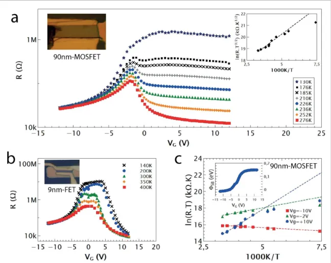
Figure 1. Metal-hBN-PdSe2FETs. Optical image of S43 PdSe2-MOSFET ((a) left inset with L× W = 10 × 25.5 µm,
tPdSe2=90 nm), and of S02 PdSe22D-FET ((b) inset with L× W = 2.8 × 13.2 µm, tPdSe2=9 nm). Main panels of (a) and (b)
show the gate voltage dependence of their drain-source resistance at different temperatures. A strong SB develops in the electron-doped regime of S43 at low temperature; its activation process is analyzed in (c) with a Richardson law model
(dotted-lines, see main text). The extracted SB-height is plotted in (c) (inset); it shows the good work function alignment between metallic Pd and the PdSe2valence band edge in the p-doped regime and a plateau in the n-doped regime. The difference gives an
SB estimate of the PdSe2bandgap ∆SB≃ 0.14 eV. A second estimate is provided by the thermal activation analysis of S43 bulk
resistance, measured at surface depletion for VG=−1.6 V in the temperature range T = 176–300 K (right inset in (a)), using the
law RT3/2=A exp (∆
bulk/2kBT) (dashed line); it gives a bandgap ∆bulk≃ 0.15 eV.
associated with optical phonon inelastic scattering at ℏΩOP≃ 145 cm−1=18 meV [4,5,25].
We have investigated two series of transist-ors qualified as thin (tPdSe2≲ 20 nm) and thick
(tPdSe2≳ 90 nm). We focus here on one
represent-ative thick device (sample S43) shown in the inset of figure 1(a), with tPdSe2=90 nm (thBN=34 nm).
Statistical relevance of S43 is illustrated in figures SI2(a–d) according to the room-temperature transfer characteristics and typical RF admittance spectra of the thick device series. For comparison, we show in the inset of figure1(b) one representative thin device (sample S02) with tPdSe2=9 nm (thBN=47 nm).
Their micrometer sizes, specified in the caption of figure 1, match IR wavelengths. Devices are char-acterized in a cryogenic DC-40 GHz probe station, their RF scattering parameters being measured over a 5-decade (70 kHz to 40 GHz) bandwidth with a vector network analyzer (Anritsu-MS4644B). Thru-lines and dummy structures are used for CPW and stray capacitance de-embedding purposes. From the full set of scattering parameters we extract the device
admittance matrix, including the zero-bias gate-source contribution of interest for the physical char-acterization of MOSFETs [22].
3. Direct current characterization
As seen in figures1(a) and (b), S43 and S02 devices show ambipolar transport at room temperature with similar resistances at large (positive and neg-ative) doping, and a resistance maximum at a charge neutrality point (CNP) VCNP∼ −1 V. The
similarity of resistances in thin (S02) and thick (S43) doped PdSe2-transistors already suggests
prominent screening effects in bulk samples. The temperature-independent CNP shift indicates a small (n-type) bulk doping. The resistance of thin S02 in figure 1(b) eventually saturates at 10 MΩ at chan-nel depletion, due to the limited resolution of our setup.
The overall shapes of the transfer characterist-ics of S43 are qualitatively different. They show plat-eaus at positive gate voltage and low temperature 3
2D Mater. 8 (2021) 035035 R Le Goff et al
(figure1(a)) that we attribute to the buildup of a SB at the PdSe2-Pd interface due to work function
mis-match between the Pd contact and the conduction band of PdSe2. This barrier is elusive at negative gate
voltage, confirming the good alignment between the work functions of metallic Pd and bulk PdSe2. The
transfer characteristic of S43 also shows a maximum at Vg≃ −1.6 V for T ≳ 150 K, signaling the
suppres-sion of surface transport at surface charge neutrality; its temperature dependence is used below to estimate the bulk bandgap of PdSe2. Below 150 K the Schottky
contact resistance dominates over bulk resistance (see the 130 K curve in figure1(a)), blurring the resistance maximum and precluding its quantitative analysis in terms of bulk thermal activation.
To quantify SB effects in S43, we show in figure 1(c) an activation plot together with high-temperature fits (dashed lines) with the Richardson law [26]: R× T = 4π 2ℏ3 e2k Bm∗eAD exp Φ kBT , (1)
where Φ the SB height,A an effective contact area, and D < 1 an electronic transmission factor account-ing for wave-function mismatch between metallic Pd and PdSe2. Note that a factor 2 has been introduced
for the additive source and drain contributions. As seen in figure1(c), the resistance obeys equation (1) above 100 K and saturates below presumably due to quantum tunneling. The high-temperature extrapol-ate, ln (R[kΩ]T[K])∼ 13 (at VG= +10 V), agrees with
the prefactor in equation (1) takingA ∼ 0.1 µm2and
D∼ 0.01. From the slope we extract Φ(Vg),
plot-ted in the inset of figure1(c), which shows a step-wise increase from Φinv≃ −0.02 eV in the inversion
regime to Φacc≃ +0.15 ± 0.01 eV in the
accumu-lation regime (blue squares). The small negative SB extracted in the inversion regime is physically irrel-evant and discloses the absence of SB between metal-lic Pd and p− PdSe2. From the sum Φacc+ Φinv we
infer a first estimate of PdSe2bandgap: ∆SB∼ (Φacc+
Φinv)≃ 0.15 ± 0.01 eV.
We have also performed an analysis of activ-ated transport at depletion (Vg≃ −1.6 V) using
the standard law for intrinsic bulk semiconductors,
RT3/2=A exp (∆
bulk/2kBT). The analysis is limited
to a reduced temperature range T = 150–300 K where a the resistance peak at surface charge neutrality is vis-ible, securing a negligible contribution of contact SB effects. We deduce an estimate of the bandgap ∆bulk=
0.15 eV. A similar analysis performed on S02 yields a somewhat larger ∆bulk≃ 0.3 eV. This blueshift of the
electronic band gap is in line with the band gap value of 0.57 eV for a slightly thinner PdSe2 flake (6.8 nm-thick) reported in Ref. [7], also based on an Arrhenius plot. These values remain below the ultimate theor-etical expectation ∆≃ 1.3 eV for single layer PdSe2.
Based on these two independent determinations, we
conclude that transport bandgap of semi-bulk PdSe2
does not completely vanish but rather saturates at ∆PdSe2=0.15 eV, consistently with theoretical
pre-diction in [4]. Note that while the SB is used here for bandgap characterization purpose, it can be min-imized by appropriate contact engineering [27] for applications.
4. High-frequency admittance
spectroscopy
Field-effect capacitance is a well established charac-terization technique of semiconductor devices [19]. It can be performed in capacitors (MOSCAPs) or tran-sistors (MOSFETs). MOSCAPs are commonly made of silicon [28], or narrow-bandgap InAs [29] semi-conductors, with a top gate and a thin oxide insu-lator, distinctively called MOS devices. The gate capa-citance is generally measured between the top gate and the (weakly) doped bulk. Here we use an in-plane variant of admittance spectrocopy for a long channel transistor geometry, taking into account the Schot-tky contact impedance. This variant is similar to pre-vious capacitor modeling that has been introduced for gate capacitance spectroscopy to study graphene electronic compressibility [22] and used to char-acterize high-mobility hBN-encapsulated graphene devices (including plasma-resonant capacitors) [30], the topological Dirac states at the surface of Bi2Se3-tetradymites [33, 34], the interface states of topo-logical heterojunctions between normal and inver-ted HgTe/CdHgTe semiconductors [31], as well as the edge states of strained HgTe quantum wells [32]. The complex gate-source admittance is meas-ured over a broad frequency range allowing for a combined in-situ characterization of gate capacit-ance CG(VG) and channel conductivity σ(VG). For
ideal carrier injection in the channel, the admit-tance spectrum reflects a crossover from an elast-ance (1/CG) dominated regime at low frequency
to a lattice-friction dominated regime at high fre-quency. Such an RF crossover from elastic-dominated to friction-dominated response is quite general and has been previously reported in the context of vor-tex matter dynamics in superconductors [35–37]. In atomically thin 2D materials, screening is negligible and one can readily extract from CG the quantum
compressibility contribution CQ=e2DOS in series
with the geometrical capacitance Cgeo. This provides
in turn a determination of the chemical potential
EF=
´
(CG/Cgeo− 1)dVgand the diffusion constant D = σ/CQ, yielding a genuine scattering
spectro-scopy encoded in the D(EF) dependence [31]. For
massive PdSe2 carriers, the 2D density of states in
the surface layer, DOS = m∗/πℏ2∼ 1014cm−2eV−1, is large such that CQ≫ Cgeo, and the gate-voltage
dependence of CG mostly stems from series
dielec-tric channel contributions. These contributions read
2D Mater. 8 (2021) 035035 R Le Goff et al
Figure 2. Zero bias gate admittance spectraI[YGS](f ) (blue circles) andR[YGS](f ) (red squares) of PdSe2-MOSFET-S43 at
T = 176 K (a), (c) and T = 294 K (d), (f). These typical spectra correspond to inversion (a), (d), depletion (b), (e) and accumulation (c)–(f) regimes. Solid lines are fits to equation (2) according to the lumped element circuit sketched in (b) which includes: the resistance r = R/L = 1/σW and capacitance cQ=CQ/W, the hBN insulator capacitance chBN=ChBN/W, and the
Schottky-contact resistance RSBand capacitance CSB∼ 30 fF, corresponding to a Schottky surface capacitance of the
Pd/n− PdSe2interface on the order of cSB∼ 1 fF µm−2. Spectra show a crossover at few∼ 0.1–10 GHz between a capacitive
regime,R[YGS]∝ f2≪ I[YGS]≃ 2 πfCG, and an evanescent wave regime,R[YGS]≃ I[YGS]∝
√
f. The SB contribution appears as a low-frequency crossover at fSB∼ 1/RSBCSB∼ 10 MHz in (c).
CPdSe2≈ ϵPdSe2/δdep/inv, with δdepthe depletion-layer
depth at neutrality, and δinvthat of the p+-n junction
in the inversion regime.
Figure 2 shows typical RF admittance spectra of the PdSe2 n-MOSFET S43. The gate admittance
YGS(ω) = Y12(ω) is reported both at room
tem-perature T = 294 K (d)–(f) and low temtem-perature
T = 176 K (a,c). Negative and positive gate voltages
correspond to (hole) inversion and (electron) accu-mulation regimes. A room-temperature depletion spectrum, for Vg∼ −1 V, is shown in panel (e). Also
shown in the figures are theoretical fits with a 1D charge diffusion model [22,32] based on a lumped-element description (sketched in figure2(b):
YGS(ω) = 1− e−γL ZD+Z0 1 + ΓSexp−γL 1− ΓDΓSexp−2 γL , (2) where Z0= √ r jcgω and γ = √
jrcgω are the line
impedance and propagation constant respectively, with r = R/L and cg=Cg/L the resistance and gate
capacitance per unit length. ZSand ZDare the source
and drain contact impedance, and ΓD=ZZDD−Z+Z00 ΓS=
ZS−Z0
ZS+Z0 are the reflection coefficients at the drain and
source contact respectively. The contact impedance
is modeled as ZSB= (R−1SB +jCSBω)−1and the
chan-nel conductivity is σ = (rW)−1. As seen in figures2(a, c–f), the 1D-model (solid lines) captures well the 4-decades admittance spectra, both at room temperat-ure (d–f) and in the inversion/accumulation regimes at low temperature (a,c). It fails describing the
low-T depletion regime in figure2(b) when both surface-layer and bulk transport are suppressed. Similarly, it also fails describing S02 admittance spectra for most of the doping range (not shown). The 1D response is characterized by a crossover frequency few(VG)∼
1 GHz between a low-frequency capacitive regime,
I(YGS)∝ f and R(YGS)∝ f2, and a high-frequency
regime,R(YGS)≃ I(YGS)∝ f1/2, which is
character-istic of evanescent waves in diffusive media. In the depletion regime (figure 2(e)), few drops to a finite
0.1 GHz value controlled by the small, thermally activated, bulk conduction. The transport crossover frequency few acts as a cutoff frequency for
photo-transistors above which photo-carrier detection is limited to the very vicinity of contacts, within a length Re γ−1≪ L.
Using a model fitting for each gate bias point (see the supplementary videos for T=176K and T=300K), we perform somehow a ”radiography” of 5
2D Mater. 8 (2021) 035035 R Le Goff et al
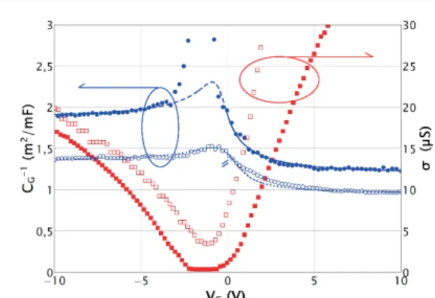
Figure 3. Gate voltage dependence of channel conductance
σand capacitance CGdeduced from RF gate capacitance
spectroscopy in figure2. The inverse capacitance (called elastance) obeys C−1G (VG) =C−1hBN+C−1PdSe
2(blue symbols),
where ChBN≈ CAL≃ 0.74 mF m−2(ϵhBN≃ 3.2ϵ0) is the
hBN dielectric contribution. Note that 294 K elastance data have been down shifted by 0.25 m2mF−1for clarity. The
elastance step between accumulation and depletion regimes measures the charge-depletion depth (see main text). Blue dashed and dotted lines are empirical fits used to extrapolate the depletion capacitance value. The conductivity σ(VG) (red symbols) reveals the ambipolar
response of the channel. Difference between 294 and 176 K data highlights the contribution of bulk thermal carriers and allows extracting T-independent mobilities: µe≃ 110 cm2V−1s−1and µh≃ 40 cm2V−1s−1.
the MOSFET and we extract the deembedded contact and channel resistances. In supplementary inform-ations (section3), they are analyzed with the same Richardson and Arhhenius plots used in DC (see section3). Both analyses confirm a bandgap value of 0.15 eV and the consistency of DC and RF responses. But we can now push our analysis further, by extracting accurate values of gate capacitance CG(VG)
and channel resistivity σ−1(VG), as shown in figure3.
At room temperature, the contact impedance YSB−1 is reduced and YGS is mostly dominated by the
chan-nel contribution. The situation is different at low-temperature, specifically in the accumulation regime (VG>0), where contact resistance was shown to be
overwhelming at DC (see figure1(a)). Its signature is a low-frequency deviation from the 1D propaga-tion, below a SB cutoff frequency fSB∼ 1/RSBCSB∼
10 MHz. Above fSB, the large contact resistance
(RSB∼ 1 MΩ), opaque to DC, is bypassed by the
contact capacitance (CSB∼ 30 fF) and one recovers
a diffusive channel admittance response. A proper account of RSBand CSBin equation(2) allows
extract-ing reliable values of CGand σ. By deembedding
con-tact contributions, figure3illustrates the temperat-ure effect on the channel elastance 1/CG=1/ChBN+
1/CPdSe2(VG)and the ambipolar conductivity.
Let us focus first on the room-temperature data (empty symbols) in figure 3. Channel conductivity (empty red squares) depicts, with an enhanced pre-cision compared to the DC data in figure1(a), the ambipolar character and the strong gate modulation of the PdSe2-MOSFET. It peaks at σ−1≃ 280 kΩ
in the depletion regime (Vg≃ −0.7 V), and drops
down to σ−1≃ 5 kΩ in the accumulation regime (Vg= +10 V), and σ−1≃ 50 kΩ in the inversion
regime (VG=−10 V). Carrier mobility is fair, with µacc.≃ 110 cm2V−1 s−1and µinv.≃ 40 cm2V−1s−1,
approaching the µ≃ 250 cm2 V−1 s−1 value
repor-ted in PdSe2 FETs after annealing [4, 5]. Gate
elastance (blue circles, note that data are shifted by −0.25 m2mF−1 for clarity) is characteristic of
n-MOSFETs [19,28,29]: it saturates in the accumu-lation regime at the (nominal) gate insulator value
CG≈ ChBN≃ 0.74 mF m−2, takes a minimum CG≃
0.52 mF m−2 at depletion, and increases to a plat-eau CG≃ 0.56 mF m−2 characteristic of an
inver-sion regime [19]. From the additivity of insulator (1/ChBN) and semiconductor (1/CPdSe2) elastance
contributions, we deduce CPdSe2≃ 1.75 mF m−2 at
depletion and CPdSe2≃ 2 mF m−2 in the inversion
regime. Relying of the theoretical estimate ϵPdSe2=
3ϵ0 [38], we infer δdep≃ 15 nm and δinv≃ 13 nm.
These small screening lengths, which are consist-ent with the Debye length LD=
√
kBTϵPdSe2/e2ND≳
7 nm for a bulk doping ND≲ 1 1017cm−3, secure
the MOSFET interpretation of our 90 nm-thick S43 device, and justify the qualitative difference between our thin and thick transistor series.
The difference between 294 and 176 K data in figure 3 illustrates thermal effects on mobility and carrier density. As expected the capacitance gate mod-ulation is more contrasted at 176 K due to a smal-ler contribution of the thermal carriers to screen-ing. To quantify the first effect we cannot rely on direct measurement of CG at depletion due to the
above-mentioned poor quality of the fits. Instead, we have used a three-parameters empirical inter-polation formula, C−1g (Vg) =C−1g (+10 V)− atanh
[(Vg− VCNP)/b] + c/
√
b2+ (V
g− VCNP)2where a, b
and c encode respectively for the capacitance step between depletion and accumulation, the amplitude and width of the capacitance dip at neutrality. Catching the room temperature CG(VG)data
(dot-ted blue line), it is used to fit 176 K data over the inversion/accumulation regimes (dashed blue line). With this procedure we infer δinv≃ 15 nm
and δdep≃ 20 nm at 176 K. Temperature effect on
σ(VG) is also instructive: room-temperature data
are mainly upshifted by a constant amount ∆σ≃ 3 µS with respect to 176 K data, implying that: (1) the mobility is essentially T-independent as expec-ted for impurity scattering, and (2) the bulk con-tribution, which is suppressed at 176 K, is thermally activated at room temperature with a bulk resistivity
tPdSe2/∆σ≃ 3 Ohm.cm. This value is consistent with
a thermal carrier density ni(300 K)∼ 1 × 1017cm−3
for a bandgap ∆bulk=0.15 eV, and a bulk
mobil-ity µbulk≃ 20 cm2 V−1 s−1. The finite bulk
mobil-ity augurs well of a fast bulk-surface dynamics of photo-carriers under illumination as anticipated in section [1].
2D Mater. 8 (2021) 035035 R Le Goff et al
5. Conclusion
In this letter we have reported on low-bias DC transport and RF gate capacitance spectroscopy in high-quality PdSe2crystals providing qualitative and
quantitative evidence that semi-bulk van der Waals PdSe2transistors behave as genuine narrow-bandgap
MOSFETs. This extensive electronic characterization allows down-pinning relevant material parameters such as PdSe2 work function, transport bandgap,
mobility, and thermal carrier density. In particular, we have deduced a fundamental electronic bandgap of 0.15 eV in agreement with the ab initio stud-ies [4, 6]. Our work suggests that the optical gap of 0.5 eV for bulk PdSe2 reported in the literature
[7] originates from higher energy transitions and offers guidance for further IR optoelectronic applic-ations, in particular for MIR detection. Finite bias properties (not reported here) confirm the quasi-intrinsic quality of our PdSe2 transistors. However
they call for a different out-of-equilibrium phys-ics (phonon-induced velocity saturation, self heat-ing, etc) which is beyond the scope of the present paper.
The demonstration of PdSe2-MOSFETs opens
new perspectives for applications of 2D materials in high-speed optoelectronics including ultra broad-band optical detectors covering the MIR range. The present demonstration of GHz electronic bandwidth at the MIR-relevant 10 µm length scale, put in per-spective with literature photo-detection measure-ments of an optical gain G = 700 A W−1[15], opens an avenue to PdSe2MOSFETs for room-temperature
monolithic broadband and high-speed sensing, com-peting the extensively used CdHgTe detectors [39].
Data availability statement
The data that support the findings of this study are available upon reasonable request from the authors.
Acknowledgments
Authors acknowledge fruitful discussions with A Vasanelli and Y Guldner and thank M Pala for proofreading the manuscript before submission. The research leading to these results has received partial funding from the European Union ‘Horizon 2020’ research and innovation programme under Grant Agreement No. 881603 ‘Graphene Core’, from the ANR-2018-CE08-018-05 ‘BIRDS’. R Le Goff thanks Thales Systèmes Aéroportés for the CIFRE Grant No. 2016/1294 funding.
ORCID iDs
Z Liuhttps://orcid.org/0000-0002-8825-7198 K Watanabe https://orcid.org/0000-0003-3701-8119 B Plaçaishttps://orcid.org/0000-0003-2408-7393 E Baudin https://orcid.org/0000-0003-3694-9640References
[1] Wang Q H, Kalantar-Zadeh K, Kis A, Coleman J N and Strano M S 2012 Electronics and optoelectronics of two-dimensional transition metal dichalcogenides Nat. Nanotechnol.7 699
[2] Schwierz F, Pezoldt J and Granzner R 2015 Two-dimensional materials and their prospects in transistor electronics Nanoscale7 8261
[3] Rasmussen F A and Thygesen K S 2015 Computational 2D materials database: electronic structure of transition- metal dichalcogenides and oxides J. Phys. Chem. C119 13169
[4] Chow W L et al 2017 High mobility 2D palladium diselenide field-effect transistors with tunable ambipolar characteristics Adv. Mater.29 1602969
[5] Oyedele A D et al 2017 PdSe2: pentagonal two-dimensional
layers with high air stability for electronics J. Am. Chem. Soc.
139 14090
[6] Sun J, Shi H, Siegrist T and Singh D J 2015 Electronic, transport and optical properties of bulk and mono-layer PdSe2Appl. Phys. Lett.107 153902
[7] Zhang G et al 2019 Optical and electrical properties of two-dimensional palladium diselenide Appl. Phys. Lett.
114 253102
[8] Koppens F H L, Mueller T, Ph A A, Ferrari C, Vitiello M S and Polini M 2014 Photodetectors based on graphene, other two-dimensional materials and hybrid systems Nat. Photon.
9 780
[9] Huang P et al 2020 Ultra-long carrier lifetime in neutral graphene-hBN van der Waals heterostructures under mid-infrared illumination Nature Commun.
11 863
[10] Hamidouche L, Montanaro A, Rostischer M, Poupet B, Taniguchi T, Watanabe K, Plaçais B, Baudin E and Legagneux P 2021 Opto-electronic mixing in high mobility graphene ACS Photon.8 369
[11] Qin D, Yan P, Ding G, Ge X, Song H and Gao G 2018 Monolayer PdSe2: a promising two-dimensional
thermoelectric material Sci. Rep.8 2764
[12] Yu X et al 2018 Atomically thin noble metal dichalcogenide: a broadband mid-infrared semiconductor Nature Comm.
9 1545
[13] Guo C et al 2020 Anisotropic ultrasensitive PdTe2-based phototransistor for room-temperature long-wavelength detection Sci. Adv.6 eabb6500
[14] Di Bartolomeo A et al 2019 Pressure-tunable ambipolar conduction and hysteresis in ultrathin palladium diselenide field effect transistors Adv. Func. Mater.29 1902483
[15] Liang Q et al 2019 High-performance, room temperature, ultra broadband photodetectors based on air stable PdSe2
Adv. Mater.31 1807609
[16] Zeng L-H et al 2019 Controlled synthesis of 2D palladium diselenide for sensitive photodetector applications Adv. Funct. Mater.29 1806878
[17] Lin Y C, Yamaguchi H, Chang E Y, Hsieh Y C, Ueki Y M, Hirayama Y and Chang C Y 2007 Growth of
very-high-mobility AlGaSb/InAs high-electron-mobility transistor structure on Si substrate for high speed electronic applications Appl. Phys. Lett.90 023509
[18] Sorger V J and Maiti R 2020 Roadmap for
gain-bandwidth-product enhanced photodetectors: opinion Opt Mater Express10 2192
[19] Hu C C 2009 Modern Semiconductor Devices for Integrated Circuits 1st edn (New Jersey: Pearson) p 351
[20] Liu X et al 2021 Temperature-sensitive spatial distribution of defects in PdSe2flakes (arXiv:2104.06642)
[21] Taniguchi T and Watanabe K 2007 Synthesis of high-purity boron nitride single crystals under high pressure by using Ba-BN solvent J. Cryst. Growth303 525
2D Mater. 8 (2021) 035035 R Le Goff et al
[22] Pallecchi E, Betz A C, Chaste J, Fève G, Huard B, Kontos T, Berroir J-M and Plaçais B 2011 Transport scattering time probed through rf admittance of a graphene capacitor Phys. Rev. B83 125408
[23] Lide R 2008 CRC handbook of chemistry and physics J. Am. Chem. Soc. 130 1
[24] Liu X, Zhou H, Yang B, Qu Y and Zhao M 2017 Strain-modulated electronic structure and infrared light adsorption in palladium diselenide monolayer Sci. rep.
7 39995
[25] Puretzky A A, Oyedele A D, Xiao K, Haglund A V, Sumpter B G, Mandrus D, Geohegan D B and Liang L 2018 Anomalous interlayer vibrations in strongly coupled layered PdSe22D Mater.5 035016
[26] Richardson O W 1901 On the negative radiation from hot platinum Phil. Camb. Phil. Soc. 11 286
[27] Oyedele A D et al 2019 Defect-mediated phase transformation in anisotropic two-dimensional PdSe2
crystals for seamless electrical contacts J. Am. Chem. Soc.
141 22, 8928
[28] Lo S-H, Buchanan D A and Taur Y 1999 Modeling and characterization of quantization, polysilicon depletion and direct tunneling effects in MOSFETs with ultrathin oxides IBM J. Res. Dev.43 327
[29] Wang S-W et al 2015 Field-effect mobility of InAs surface channel nMOSFET with low dit scaled Gate-Stack IEEE Trans. Elec. Dev.62 2429
[30] Graef H et al 2018 Ultra-long wavelength Dirac plasmons in graphene capacitors J. Phys. Mater.1 01LT02
[31] Inhofer A et al 2017 Observation of Volkov–Pankratov states in topological HgTe heterojunctions using high-frequency compressibility Phys. Rev. B96 195104
[32] Dartiailh M C et al 2020 Dynamical separation of bulk and edge transport in HgTe-based 2D topological insulators Phys. Rev. Lett.124 076802
[33] Inhofer A et al 2018 RF-quantum capacitance of topological insulator Bi2Se3 in the bulk depleted regime for field-effect transistors Phys. Rev. Appl.9 024022
[34] Inhofer A et al 2019 RF compressibility of topological surface and interface states in metal-hBN-Bi2Se3capacitors J. Phys.
Mater.2 04400
[35] Placais B, Mathieu P, Simon Y, Sonin E B and Traito K B 1996 Continuum electrodynamics of type-II superconductors in the mixed state: the dc and ac response Phys. Rev. B54 13083
[36] Lütke Entrup N, Plaçais B, Mathieu P and Simon Y 1997 Depinning transition in type-II superconductors Phys. Rev. Lett.79 2538
[37] Lütke-Entrup N, Plaçais B, Mathieu P and Simon Y 1998 RF-studies of vortex dynamics in isotropic type-II superconductors Physica B255 75
[38] Deng S, Li L and Zhang Y 2018 Strain modulated electronic, mechanical and optical properties of the monolayer PdS2, PdSe2and PtSe2for tunable devices ACS Appl. Nano Mater.
1 1932
[39] Gravrand O, Mollard L, Boulade O, Moreau V, Sanson E and Destefanis G 2012 Ultralow-dark-current CdHgTe FPAs in the SWIR range at CEA and sofradir J. Electron. Mater.
41 2686
 (blue circles) and R [Y GS ]( f) (red squares) of PdSe 2 -MOSFET-S43 at T = 176 K (a), (c) and T = 294 K (d), (f)](https://thumb-eu.123doks.com/thumbv2/123doknet/14559715.538234/7.892.179.828.92.554/figure-zero-admittance-spectra-circles-squares-pdse-mosfet.webp)