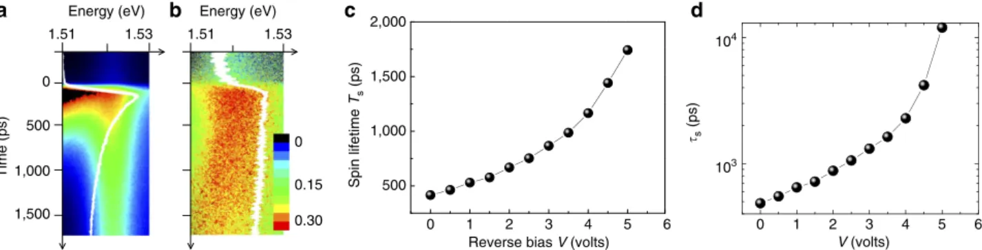
Gate control of the electron spin-diffusion length in semiconductor quantum wells
Texte intégral
Figure


Documents relatifs
L’archive ouverte pluridisciplinaire HAL, est destinée au dépôt et à la diffusion de documents scientifiques de niveau recherche, publiés ou non, émanant des
La maîtrise des risques infectieux associés aux soins (IAS) dont les problèmes d’accidents exposant au sang (AES) le personnel de santé ainsi que les défections
Dans ce contexte, l’apport envisagé avec ce travail de thèse est de collaborer à la conception optimale d’un système de conversion de l’énergie
In contrast, Li' ions are shown to be fast diffusing impurities in AgBr with vacancy jump frequencies larger than those of the host cations.. - The study of
Abstract.- The energy dependence of the electron relaxation time for electron-phonon scattering is included in the calculation of the electrical resistivity of the polyvalent,
Abstract 2014 The orientational dependence of the diffusion constant D of electronic spins has been determined for single crystals of the radical cation salt
of a slow exchange process among magnetically unequivalent sites, each one corresponding to a particular orientation of the magnetic field with respect to the principal axes of the
INDIRECT MEASUREMENTS OF THE IMPURITY ELECTRON SPIN RELAXATION TIME BY NUCLEAR SPIN LATTICE RELAXATION IN CdMn ALLOYS.. Journal de Physique Colloques, 1971, 32
