HAL Id: hal-00332055
https://hal.archives-ouvertes.fr/hal-00332055v2
Submitted on 30 Jan 2009
HAL is a multi-disciplinary open access
archive for the deposit and dissemination of
sci-entific research documents, whether they are
pub-lished or not. The documents may come from
teaching and research institutions in France or
abroad, or from public or private research centers.
L’archive ouverte pluridisciplinaire HAL, est
destinée au dépôt et à la diffusion de documents
scientifiques de niveau recherche, publiés ou non,
émanant des établissements d’enseignement et de
recherche français ou étrangers, des laboratoires
publics ou privés.
High domain wall velocity at zero magnetic field induced
by low current densities in spin-valve nanostripes
Stefania Pizzini, Vojtech Uhlir, Jan Vogel, Nicolas Rougemaille, Sana Laribi,
Vincent Cros, Erika Jimenez, Julio Camarero, Carsten Tieg, Edgar Bonet, et
al.
To cite this version:
Stefania Pizzini, Vojtech Uhlir, Jan Vogel, Nicolas Rougemaille, Sana Laribi, et al.. High domain wall
velocity at zero magnetic field induced by low current densities in spin-valve nanostripes. Japanese
Journal of Applied Physics, part 2 : Letters, Japan Society of Applied Physics, 2009, 2, pp.023003.
�10.1143/APEX.2.023003�. �hal-00332055v2�
in Spin Valve Nanostripes
Stefania Pizzini,1 Vojtˇech Uhl´ıˇr,1, 2 Jan Vogel,1 Nicolas Rougemaille,1 Sana Laribi,3 Vincent Cros,3
Erika Jim´enez,4 Julio Camarero,4, 5 Carsten Tieg,6 Edgar Bonet,1 Marlio Bonfim,7, 1 Richard
Mattana,3 Cyrile Deranlot,3 Fr´ed´eric Petroff,3 Christian Ulysse,8 Giancarlo Faini,8 and Albert Fert3
1Institut N´eel, Centre National de la Recherche Scientifique (CNRS)
and Universit´e Joseph Fourier, B.P.166, 38042 Grenoble, France
2Institute of Physical Engineering, Brno University of Technology, 61669 Brno, Czech Republic 3Unit´e Mixte de Physique CNRS/Thales and Universit´e Paris Sud 11, 91767 Palaiseau, France
4Dpto. F´ısica de la Materia Condensada and Inst. Nicol´as Cabrera,
Universidad Aut´onoma de Madrid, 28049 Madrid, Spain
5Instituto Madrile˜no de Estudios Avanzados en Nanociencia (IMDEA-Nano), Campus de Cantoblanco, 28049 Madrid, Spain 6European Synchrotron Radiation Facility, rue Jules Horowitz, BP200, 38043 Grenoble, France
7Departamento de Engenharia El´etrica, Universidade Federal do Paran´a, 81531-990 Curitiba PR, Brasil 8CNRS, PhyNano Team, Laboratoire de Photonique et de Nanostructures, route de Nozay, F-91460 Marcoussis, France
Current-induced magnetic domain wall motion at zero magnetic field is observed in the permalloy layer of a spin-valve-based nanostripe using photoemission electron microscopy. The domain wall movement is hampered by pinning sites, but in between them high domain wall velocities (exceeding 150 m/s) are obtained for current densities well below 1012
A/m2
, suggesting that these trilayer systems are promising for applications in domain wall devices in case of well controlled pinning positions. Vertical spin currents in these structures provide a potential explanation for the increase in domain wall velocity at low current densities.
Moving magnetic domain walls using electric currents via spin-torque effects rather than using a magnetic field is one of the recent exciting developments in spintronics1.
Since the prediction of spin-torque effects2, many
ex-perimental3,4,5,6,7,8,9,10,11,12,13,14,15and theoretical16,17,18
works have been dedicated to the study of current-induced domain wall motion (CIDM). Besides fundamen-tal investigations, the use of domain walls in logic19 and
memory20 devices has already been proposed. Low
cur-rent densities and high domain wall (DW) velocities at zero magnetic field are required for future applications.
Direct evidence of CIDM at zero field has been re-ported for several nanostripe systems, including permal-loy (FeNi)6,11, magnetic semiconductors9 and systems
with perpendicular magnetization7,12,14,15. For the
com-monly used FeNi system, the critical current densities are not much below 1012 A/m2 at zero magnetic field8,11,
associated with DW velocities going from some m/s up to about 100 m/s11. Much lower critical currents are
found for magnetic semiconductors like GaMnAs (about 1 × 10⁹ A/m2) because of the low magnetic moments,
but the observed DW velocities are small (< 1 m/s)9.
Moreover, these materials are not ferromagnetic at room temperature. Low current density values are also found in spin-valve-based nanostripes with either in-plane3,10
or perpendicular anisotropy7. Additionally, transport
measurements in FeNi/Cu/Co trilayers show CIDM in-duced by subnanosecond current pulses5, indirectly
indi-cating high DW velocities in such spin-valve-based sys-tems. In this work, we show that in these systems CIDM at zero magnetic field can take place with high DW ve-locities (exceeding 150 m/s) at current densities well be-low 1012A/m2. These high velocities are observed only
in certain regions of the nanostripes, where domain wall
pinning is limited. Currents perpendicular to the plane in the vicinity of the DW are probably partly responsible for this increase in efficiency, which makes the trilayer systems possible candidates for spintronic applications based on CIDM if pinning can be controlled.
We observed domain wall motion in the FeNi layer of 400 nm wide FeNi (5 nm)/Cu (8 nm)/Co (7 nm)/ CoO (3 nm) nanostripes, by using Photoemission Elec-tron Microscopy (PEEM) combined with X-ray Magnetic Circular Dichroism (XMCD)21. The Cu spacer layer is
chosen to be sufficiently thick to avoid any interlayer ex-change coupling or magnetostatic orange-peel coupling between the magnetic layers. The nanostripes were pro-cessed from film stacks grown by sputtering on high re-sistivity Si substrates, combining electron beam lithogra-phy and lift-off technique. They were patterned in zigzag shapes with angles of 90 and 120◦[see Fig. 1(a)]. Contact
electrodes made of Ti/Au were subsequently deposited using evaporation and lift-off technique.
The samples were mounted on a sample holder that al-lows both magnetic field pulses and current pulses to be applied. For field pulses, we used a combination of double stripline-like microcoils and a home-made pulsed current supply22. Nanosecond magnetic field pulses could be
ap-plied in the plane of the stripes, perpendicular to the long axis of the zigzag (see Fig 1). Current pulses were injected into the nanostripes using a generator providing voltage pulses with 4 ns risetime and tunable length. The current flowing through the stripes was deduced from the voltage measured over the 50 Ω entrance of a 6 GHz os-cilloscope connected in series with the stripes.
Our XMCD-PEEM measurements were performed at the European Synchrotron Radiation Facility beamline ID08. In order to avoid discharges from the objective
2 lens of our Focus IS-PEEM, which is at a distance of
2 mm from the sample, the voltage on the objective lens was kept below 4.2 keV, limiting the spatial resolution to about 0.7 µm. In order to image the domain structure in the FeNi layer, the x-ray energy was tuned to the Ni L3absorption edge (852.8 eV). To optimize the magnetic
contrast, the difference between two consecutive images obtained with 100% left- and right-circularly polarized x-rays was computed. The presence of a rather thick Cu spacer (8 nm) layer, combined with the limited escape depth of the secondary electrons, prevented images of the Co domain structure to be taken.
x -r a ys 5 µm H (a)
M
M
(b)FIG. 1: Topographic (a) and magnetic (b) PEEM images of a 400 nm wide spin-valve-like nanostripe with a zigzag angle of 90◦, taken at the Ni L
3-edge. A static in-plane magnetic
field of 400 mT was applied perpendicular to the incoming X-ray beam before the measurements, as indicated by the arrow at the top of (b). In (b), white (black) contrast corresponds to domains having a magnetization component parallel (an-tiparallel) to the incoming x-ray direction, as indicated by the black and white arrows. The horizontal bar in the upper part of the images is one of the gold contacts for current injection. Before introducing the samples into the PEEM micro-scope, we applied an in-plane magnetic field of 400 mT perpendicularly to the zigzag long axis. The remanent magnetic state obtained for a 400 nm wide, 90◦ angle
zigzag nanostripe is shown in Fig. 1(b). The contrast is given by the projection of the magnetization on the beam direction, i.e., white (black) domains have their magnetization pointing downwards (upwards), along the stripes. The magnetization is nearly saturated in the straight sections, but a black-white-black-white contrast is visible at the bends. The magnetization in the straight sections of the buried Co layer is expected to be paral-lel to the FeNi magnetization, leading to domain walls at the bends. These head-to-head or tail-to-tail domain walls lead to strong magnetostatic effects that induce a local antiparallel alignment between Co and FeNi layers in the vicinity of the Co DW23. In the straight sections,
these magnetostatic interactions caused by Co domain walls should not be present.
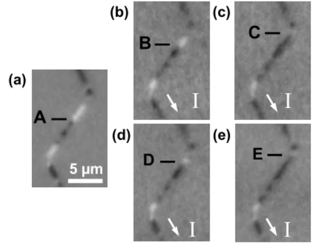
In Fig. 2, we show current-induced DW motion in a 400 nm wide stripe with zigzag angles of 120◦. The
ini-tial domain structure was obtained after application of several magnetic field and current pulses. Domain wall pinning in these structures is quite strong, and several at-tempts to induce domain wall motion with current pulses
were made before reproducible motion could be obtained. The domain structure in Fig. 2(a) could be obtained re-producibly by applying 50 ns long magnetic field pulses in the plane of the samples, to the left in the figure, with an amplitude of 50 mT. Starting from this initial state, we applied current pulses with different amplitudes and lengths, in order to determine the DW velocity and the threshold current in this section. Figure 2(b) shows the domain structure obtained after applying one 100 ns long current pulse with an amplitude of +2 mA, a value be-low which no DW motion was detected for these rela-tively short pulses. This threshold current pulse causes a displacement of the domain wall from position A to position B in the images. A consecutive pulse with the same amplitude and length induces a further movement of the same domain wall in the same direction, from B to C [Fig. 2(c)]. Note that in these images only one DW moves for the applied amplitude of the current, showing that the pinning strengths can strongly differ at different positions in the nanostripe. The free motion of the FeNi DW over section A-C in Fig. 2 indicates that pinning in this section is relatively small.
A
B
C
(a) (b) (c)I
I
5 µmD
E
I
I
(d) (e)FIG. 2: XMCD-PEEM images of the FeNi layer of a 400 nm wide spin-valve-like nanostripe with a zigzag angle of 120◦.
(a) gives the initial domain state, obtained after applying an in-plane 50 mT magnetic field pulse perpendicular to the long direction of the stripe. (b) and (c) show the images after application of one, resp. two 100 ns long current pulses of +2 mA starting from the domain state of (a). The indicated DW moves from position A to position B with the first pulse, and from B to C with the second pulse. (d) and (e) show images obtained after application of one 15 ns pulse of +5 mA and one 20 ns pulse of +5 mA, respectively, in both cases starting from the initial state of (a). The 15 ns pulse makes the DW move from position A to D, the 20 ns pulse causes a motion from A to E.
The first pulse causes a CIDM of (1.75 ± 0.2) µm, the second pulse (1.92 ± 0.2) µm, resulting in a domain wall velocity of about (18 ± 2) m/s. The current density in the FeNi layer corresponding to the +2 mA pulse is 2 × 10¹¹A/m2 if we consider a uniform current
suppose that the current density is proportional to the conductivity in each layer10. The value of 2 × 10¹¹A/m2
gives thus an upper bound for the current density in the FeNi layer. In Figs. 2(d) and 2(e), we show results of mea-surements using current pulses with the maximum avail-able amplitude of 5 mA (corresponding to a current den-sity of 5 × 10¹¹A/m2in the FeNi layer, or 1 × 10¹¹A/m2
for non-uniform current distribution) and lengths of 15 and 20 ns, in both cases starting from the initial state shown in Fig. 2(a). The CIDM for the 15 and 20 ns pulses are (2.7 ± 0.2) µm and (3.4 ± 0.2) µm, showing that in this section of the nanostripe the displacement is about proportional to the pulse length. The result-ing DW velocities are (180 ± 10) and (170 ± 10) m/s, respectively. This result clearly shows that for this tri-layer system the current-induced domain wall velocities between pinning sites are above literature values for sin-gle FeNi layers11, for current densities that are at least
a factor two smaller. The above results for strongly dif-ferent pulse lengths indicate that for this section the dis-placements are proportional to the pulse length. This suggests that DW movement takes place only during the current pulse and that movements after the current pulse, for instance due to attractive potential wells, are small. Domain wall pinning can be caused by edge roughness induced by the lithography, stray fields of domain walls in the Co layer, interface roughness or grain boundaries. Scanning electron microscopy of our structures indicates a lateral roughness smaller than 1 nm. Roughness of the Cu/FeNi interface should be small with respect to the total FeNi layer thickness of 5 nm. Pinning at grain boundaries could be reduced using amorphous layers of CoFeB instead of FeNi10.
In general, experimental results of current-induced DW dynamics are described (at least qualitatively) using a phenomenological model with two components for the spin transfer torque, i.e., the adiabatic and the non-adiabatic torque. In the simplest approach of a 1D domain wall model18, the DW velocity is expressed as
vDW = βαu where u is the rate of spin angular momentum
transfer from the conduction electrons to the local mo-ments in the domain wall [u = JP gµB/(2eMS) where J
is the current density and P its polarization rate18].
Sev-eral experiments indicate a value of the non-adiabaticity parameter β close to α, the damping term24,25.
How-ever, recently Hayashi et al.11 observed a maximum DW
velocity of 110 m/s (for J = 1.5 × 10¹² A/m2) at zero
magnetic field in 300 nm FeNi nanostripes. This velocity is larger than the spin angular momentum transfer rate u for any P < 1 (for P = 0.7, u is about 75 m/s and
β
α ≈ 1.5). Using the same parameters, our current
den-sity J ≈ 5 × 10¹¹A/m2would lead to a spin transfer rate
u of about 25 m/s. The only way to explain our mea-sured velocity of 175 m/s within this model would be to assume aβαof about 7. Such a very large non-adiabaticity seems unlikely and other spin transfer mechanisms must be considered to explain our high DW velocities.
A specificity of our spin-valve structures is that part of the incident spin flux in the FeNi layer is transformed, in the region around the DW, into spin accumulation in the Cu and Co layers. This spin accumulation in the Cu spacer layer below the DW induces a vertical (Cur-rent Perpendicular to the Plane or CPP) spin cur(Cur-rent that flows into the DW and exerts an additional torque on the DW. This situation is somewhat similar to that of spin transfer in the CPP geometry of magnetic pillars. Our results suggest that the yield of this additional verti-cal spin transfer channel is much higher than the yield of the in-plane spin transfer channel, as predicted recently by micromagnetic simulations on similar nanostructures containing a single DW26. Our direct observation of high
velocity current-induced DW motion confirms the poten-tial of these trilayer systems for applications in DW-based magnetic memories and logic devices.
Acknowledgments
We acknowledge the technical support of E. Wag-ner, P. Perrier, D. Lepoittevin, and L. Delrey, as well as the experimental help of S. Pairis, T. Fournier, and W. Wernsdorfer. We are grateful to A. Khvalkovskiy, A. Anane, and J. Grollier for discussions. E.J. and J.C. acknowledge financial support through projects HF2007-0071, MAT2006-13470, and CSD 2007-00010. V.U. was financially supported by the grants No. MSM0021630508 and No. KAN400100701. This work was partially sup-ported by the ANR-07-NANO-034 ‘Dynawall’.
1
C. Marrows: Adv. Phys. 54 (2005) 585.
2
L. Berger: J. Appl. Phys. 55 (1984) 1954.
3
J. Grollier, P. Boulenc, V. Cros, A. Hamzic, A. Vaur`es, A. Fert, and G. Faini: Appl. Phys. Lett. 83 (2003) 509.
4
A. Yamaguchi, T. Ono, S. Nasu, K. Miyake, K. Mibu, and T. Shinjo: Phys. Rev. Lett. 92 (2004) 077205.
5
C. Lim, T. Devolder, C. Chappert, J. Grollier, V. Cros, A. Vaur`es, A. Fert, and G. Faini: Appl. Phys. Lett. 84 (2004) 2820.
6
M. Kl¨aui, P.O. Jubert, R. Allenspach, A. Bischof,
J. A. C. Bland, G. Faini, U. R¨udiger, C. Vaz, L. Vila, and C. Vouille: Phys. Rev. Lett. 95 (2005) 026601.
7
D. Ravelosona, D. Lacour, J. Katine, B. Terris, and C. Chappert: Phys. Rev. Lett. 95 (2005) 117203.
8
M. Kl¨aui, M. Laufenberg, L. Heyne, D. Backes, U. R¨udiger, C. Vaz, J. A. C. Bland, L. Heyderman, S. Cherifi, A. Lo-catelli, T. Mentes, and L. Aballe: Appl. Phys. Lett. 88 (2006) 232507.
9
M. Yamanouchi, J. Ieda, F. Matsukura, S. Barnes, S. Maekawa, and H. Ohno: Science 317 (2007) 1726.
4
10
S. Laribi, V. Cros, M. Mu˜noz, J. Grollier, A. Hamzi´c, C. Deranlot, A. Fert, E. Mart´ınez, L. L´opez-D´ıaz, L. Vila, G. Faini, S. Zoll, and R. Fournel: Appl. Phys. Lett. 90 (2007) 232505.
11
M. Hayashi, L. Thomas, C. Rettner, R. Moriya, Y. Bazaliy, and S. S. P. Parkin: Phys. Rev. Lett. 98 (2007) 037204.
12
H. Tanigawa, K. Kondou, T. Koyama, K. Nakano, S. Ka-sai, N. Ohshima, S. Fukami, N. Ishiwata, and T. Ono: Appl. Phys. Express 1 (2008) 011301.
13
A. Vanhaverbeke, A. Bischof, and R. Allenspach: Phys. Rev. Lett. 101 (2008) 107202.
14
T. Koyama, G. Yamada, H. Tanigawa, S. Kasai, N. Ohshima, S. Fukami, N. Ishiwata, Y. Nakatani, and T. Ono: Appl. Phys. Express 1 (2008) 101303.
15
T.A. Moore, I.M. Miron, G. Gaudin, G. Serret, S. Auffret, B. Rodmacq, A. Schuhl, S. Pizzini, J. Vogel, and M. Bon-fim: Appl. Phys. Lett. 93 (2008) 262504.
16
G. Tatara and H. Kohno: Phys. Rev. Lett. 92 (2004) 086601.
17
Z. Li and S. Zhang: Phys. Rev. Lett. 93 (2004) 127204.
18
A. Thiaville, Y. Nakatani, J. Miltat, and Y. Suzuki:
Euro-phys. Lett. 69 (2005) 990.
19
D. Allwood, G. Xiong, C. Faulkner, D. Atkinson, D. Petit, and R. Cowburn: Science 309 (2005) 1688.
20
S. S. P. Parkin, M. Hayashi, and L. Thomas: Science 320 (2008) 190.
21
A. Locatelli, and E. Bauer: J. Phys.: Condens. Matter 20 (2008) 093002.
22
J. Vogel, W. Kuch, J. Camarero, K. Fukumoto, Y. Pen-nec, M. Bonfim, S. Pizzini, F. Petroff, A. Fontaine, and J. Kirschner: J. Appl. Phys. 95 (2004) 6533.
23
J. Vogel, S. Cherifi, S. Pizzini, F. Romanens, J. Camarero, F. Petroff, S. Heun, and A. Locatelli: J. Phys.: Condens. Matter 19 (2007) 476204.
24
G. S. D. Beach, C. Knutson, C. Nistor, M. Tsoi, and J. L. Erskine: Phys. Rev. Lett. 97 (2006) 057203.
25
G. Meier, M. Bolte, R. Eiselt, B. Kr¨uger, D.H. Kim, and P. Fischer: Phys. Rev. Lett. 98 (2007) 187202.
26
A. Khvalkovskiy, K. Zvezdin, Y. Gorbunov, A. Zvezdin, V. Cros, and J. Grollier, arXiv:0806.2369v1.