Commercialization of Low Temperature
Copper Thermocompression Bonding for 3D Integrated Circuits
byRaghavan Nagarajan
B.ENG. Electrical & Electronics Engineering Nanyang Technological University, Singapore, 2007
MASSACHUSMTSi INSTITTE
OF TECHNOLOGY
SEP 12 2008
LIBRARIES
SUBMITTED TO THE DEPARTMENT OF MATERIALS SCIENCE AND ENGINEERING INPARTIAL FULFILLMENT OF THE REQUIREMENTS FOR THE DEGREE OF MASTER OF ENGINEERING IN MATERIALS SCIENCE AND ENGINEERING
AT THE
MASSACHUSETTS INSTITUTE OF TECHNOLOGY SEPTEMBER 2008
© 2008 Massachusetts Institute of Technology All rights reserved
Signature of Author:....
Department of Materials Science and Engineering August 15th,2008 C ertified by : ... ... ...
X
Carl V. Thompson IIStavros Salapatas Professor of Materials Science and Engineering Thesis Co-Advisor
C ertified by : ... .
Chee Lip Gan Assistant Professor, Nanyang Technological University (NTU), Singapore
7·) Thesis Co-Advisor
Accepted by: ... ... . ... ...
Samuel M. Allen POSCO Professor of Physical Metallurgy Chair, Departmental Committee on Graduate Students
Commercialization of Low Temperature
Copper Thermocompression Bonding for 3D Integrated Circuits
by
Raghavan Nagarajan
Submitted to the Department of Materials Science and Engineering on August 15t , 2008 in Partial Fulfillment of the Requirements for the Degree of
Master of Engineering in Materials Science and Engineering
ABSTRACT
Wafer bonding is a key process and enabling technology for realization of three-dimensional integrated circuits (3DIC) with reduced interconnect delay and correspondingly increased circuit speed and decreased power dissipation, along with an improved form factor and portability. One of the most recent novel and promising wafer bonding approaches to realizing 3DIC is Low Temperature Thermocompression (LTTC) bonding using copper (Cu) as the bonding interface material. This thesis investigates the LTTC bonding approach in terms of its technological implications in contrast to other conventional bonding approaches. The various technological aspects pertaining to LTTC are comprehensively explored and analyzed. In addition to this, the commercialization potential for this technology is also studied and the economic viability of this process in production is critically evaluated using suitable cost models. Based on the technological and economic outlook, the potential for commercialization of LTTC is gauged. Thesis Supervisor: Carl V. Thompson II
DEDICATION
This work is dedicated in memory of my beloved grandfather, Mr. S.N.Sivaramakrishnan, who has been a great source of inspiration to me throughout my life. His divine blessings, compassion, unflagging support, good wishes and strong patronage have been a major driving force for me to achieve and fulfill all my endeavors in life successfully. I would like to take this opportunity to express my deepest gratitudes to him for everything he has bestowed me with.
ACKNOWLEDGEMENTS
First and foremost, I would like to convey my sincere gratitudes to both my supervisors Prof Carl V. Thompson (MIT) and Dr. Gan Chee Lip (NTU, Singapore) for their timely
guidance, useful advice, encouragement and support throughout the course of this work. I have gained a lot by interacting with them during the thesis discussion meetings and their suggestions have helped improve the quality of my work to a large extent. I have been greatly inspired by Prof. Thompson's courses in the Singapore-MIT Alliance (SMA) program and his teaching styles, his way of thinking and his approach to solving scientific problems have been fascinating. His courses have helped me look at semiconductors from a material science perspective in addition to the electronics perspective that I learnt during my undergraduate courses in Electronics Engineering at NTU. He is indeed one of my "role models" for my future ambition to join the academia. Thanks to Dr.Gan for organizing all the video conference sessions that I could use to update my thesis work to Prof.Thompson while I was here in Singapore.
Next, I would like to thank my parents Mr.Narayanaswamy Nagarajan and Mrs.Srimathi
Nagarajan for the love and affection they have always showered at me. Without their
psychological support, I would never have achieved what I intended to in life. The person I miss the most is my grandfather, Mr.S.N.Sivaramakrishnan, to whom I am dedicating this work. He has been instrumental in bringing me up since my childhood and propelling me to perform well in my research and has always stood by me during the course of my life. It is because of his constant encouragement and his divine blessings that I have been able to come up in life. Unfortunately, he is not with me today to share my happiness.
The greatest asset I have acquired through the SMA program are my friends who have become an integral part of my life. I have found some of the best friends of my life through the SMA program. They have been a major source of emotional support to me during my stay at MIT whenever I missed home and felt homesick. I have no words to express my gratitude to them. These are friends that will remain with me forever in my life and I am indeed very fortunate to have found them and I must thank the almighty for having given me such precious people. Let me take this opportunity to thank them individually. Anay (also nicknamed as "dumbass") and
Rajamouly ("Raju") are two of the "coolest" friends I have ever had and by far, the ones with the
best sense of humor. There have been many instances when I used to feel very dejected upon seeing my exam results at MIT. These two guys were the ones who comforted me all along and made me more sportive. Kunal (the one and only one who can challenge professors) has been a great advisor to me in all ways. I have benefited a lot from his advises and he is one of my true well-wishers. I know him since my undergrad days and we enjoy interacting with each other a lot.
Manik (according to me the most handsome and "skeletony" Indians I have ever seen) is one of
those soft characters whom I like talking to and making fun of very often. Kwan Wee (known as an "anti-social" person and the "grandfather" of our batch) has surprisingly been very social with me all along. He is according to me the most helpful person in our batch whom anyone could look up to when needed. He is one of those guys I admire a lot and like being scolded by him and we chat about interesting things for long hours every night disturbing each other's work. He is of a caring nature and along with Yu Yan, he helped organize various trips for our group both at MIT and in Singapore. Yu Yan and Fidelia (the youngest kid SMA has ever seen) are the two most cheerful and "enthu" girls in our batch who keep everyone around them excited and happy all the time. One thing I should admit I didn't like about Yu Yan was her desire to complete all her homework way before the deadline. Qixun ("Prof. Wee"), Beng Sheng (Mr. Handsome), "Uncle"
Song Yang, Zhoujia (fatty boy), Luo Jia (the potential "rice-eater") Man Yin ("the rich i-Phone
Ha (always smiling as her name suggests) have all been great friends of mine and we have shared
many interesting moments all along this journey. Omkar (CPE) (who is stuck with chemical reactions all the time and who ditches us for lunch and dinner whenever we call him) and
Priyanka (MST) (who can give you facts and figures up to many decimal places which are totally
irrelevant) were also part of our Indian gang and we had great fun going various places for dinner and cinema quite often while in Singapore. Vivek, my MIT roommate, is another guy who deserves mention. We had a good time as roommates at Tang Hall and enjoyed cooking delicious Indian food together.
As far as my thesis is concerned, I would like to thank Wardhana (SMA PhD) and I Made Riko (NTU PhD) who have helped me along the way with effective suggestions and provided useful reference materials for my study. The commercialization aspect of the technology investigated in this work has been largely possible because of the 3.207 module coordinated by Prof
E.A.Fitzgerald. I would like to thank him for the critical assessment of my work during the
presentations for the 3.207 course.
Finally, let me extend my thanks to the SMA office at both the MIT and Singapore side for helping out in organizing the final thesis presentation. SMA was a great experience and its success stories will continue to unwind... It is the best example of how successful distance education programs can be.
TABLE OF CONTENTS
LIST OF FIGURES 11
LIST OF TABLES 13
1. INTRODUCTION TO 3D INTEGRATED CIRCUITS 15
1.1 NEED FOR 3D INTEGRATED CIRCUITS ... ... 15
1.2 ADVANTAGES OF 3D INTEGRATED CIRCUITS ... 16
1.3 APPROACHES TO 3D INTEGRATION ... 16
2. COPPER THERMOCOMPRESSION BONDING - OVERVIEW 19 2.1 TECHNIQUES OF WAFER BONDING... 19
2.2 BONDING ARCHITECTURE... ... 21
2.2.1 VIA-FIRST & VIA-LAST PROCESS... 21
2.2.2 F2F-B2B /F2B-F2B BONDING... . . ... ... 22
2.2.3 C2C- C2W- W2W BONDING... 23
2.3 FUNDAMENTALS OF THERMOCOMPRESSION BONDING ... 25
2.3.1 HIGH TEMPERA TURE THERMOCOMPRESSION (HTTC) ... 27
2.3.2 LOW TEMPERATURE THERMOCOMPRESSION (LTTC) ... 27
2.3.3 ISSUES WITH LTTC TECHNOLOGY. ... 28
2.3.4 PROCESS SEQUEN CE FOR TCB ... 29
2.3.5 PROCESSING ISSUES IN TCB ... 30
2.3.6 ELECTRONIC IMPLICATIONS OF TCB... 33
3. PHYSICS & MECHANICS OF WAFER BONDING 35 3.1 PHYSICS & MECHANICS OF WAFER BONDING ... ... 35
3.1.1 EFFECT OF WAFER BOW... ... 37
3.1.2 EFFECT OF PA TTERNING... 37
3.1.3 EFFECT OF MATERIAL & DIMENSIONAL PARAMETERS... 38
3.1.4 EFFECT OF SURFACE ROUGHNESS & APPLIED LOAD ... 39
3.1.5 EFFECT OF SURFACE QUALITY & TEMPERATURE... . 43
,4. RELIABILITY OUTLOOK & FAILURE MECHANISMS 45 4.1 FAILURE MECHANISMS IN TCB ... 45
4.2 PACKAGING & HEAT DISSIPATION FOR 3D IC TCB DEVICES ... 48
5. MICROSTRUCTURE ANALYSIS OF BONDED INTERFACE 51 6. YIELD & RELIABILITY MODELING APPROACH FOR 3DIC 55 6.1 IMPORTANCE OF YIELD & RELIABILITY MODELING ... . 55
6.2 FACTORS AFFECTING LTTC YIELD... 55
6.3 STATISTICAL YIELD MODEL ... ... 57
7. COMMERCIALIZATION POTENTIAL -LTTC TECHNOLOGY 59 7.1 DEVICE APPLICATIONS OF 3DIC ... . ... 59
7.2 APPLICATION OF FOCUS FOR LTTC TECHNOLOGY ... 60
7.3 COST ANALYSIS ... 61
7.3.1 COMPONENTS OF COSTMODEL ... ... 61
7.3.2 ANALYSIS & JUSTIFICATION OF COSTMODEL... 63
7.3.3 SENSITIVITYANALYSIS, THRESHOLD YIELD & THROUGHPUT... 64
7.4 IP L A N D SC A PE ... 67
7.5 SUPPLY CHAIN PERSPECTIVE ... ... 69
7.6 HYPE FACTOR ... 70
7.7 FUNDING PERSPECTIVE ... ... 71
7.8 WOOING LICENSEES (CUSTOMERS) ... 72
7.9 STRATEG Y TO ADO PT... ... 72
8. COMPARISON WITH COMPETING TECHNOLOGIES 73 9. CONCLUSION 75 APPENDIX 77 A. STATISTICAL YIELD M ODEL ... ... 77
A. DEFECTS... . ... ... ... ... 77
A.2 CONTACTAREA SPOTS ... ... 77
A.3 STOCHASTIC YIELD MODEL... . ... 78
A.4 YIELD FOR M ULTIPLE DIE STACKING ... 82
A.5 CUMULATIVE YIELD OF 3DIC... ... ... 83
REFERENCES 84
LIST OF FIGURES
Fig 1.1 Heterogeneous integration of devices on a 3D IC layout platform to make SoC4.
Fig 1.2 Reduction of global interconnect length and density of interconnects for 3D IC layout' 6. Various bonding techniques for 3D integration - (a) Beam recrystallization, (b) & (c)
ig 1.3 Solid phase crystallization, (d) Processed wafer bonding1.
Fig 2.1 Adhesive bonding process using polymers such as BCB as intermediate glue layer27
Fig 2.2 Typical bonding process sequence for HTTC and LTTC bonding technology30. Fig 2.3 TCB achieved either by B2F bonding or alternative F2F-B2B bonding strategies.
Typical process sequence for F2F TCB patterned Cu layer bonding - Steps -(1) FEOL +
BEOL; (2) oxide layer deposition, patterning and Cu pad formation; (3) oxide layer recess to expose Cu pads; (4) F2F alignment; (5) Thermocompression bonding; (6) CMP to back grind top wafer and (7) lithography and patterning for TSV and probe-pads40. Illustrating the dishing effects observed in patterned Cu lines due to CMP25.
Fig 2.5 The figure on the right is the actual profilometer image used to determine the depth of a Cu dish surface.
Process sequence for wafer bonding involving the use of carrier wafer to handle thin Fig 2.6 substrates3 1.
Force-separation curve for two wafer surfaces and illustration of the bond front for Fig 3.1 bonding of bowed wafers34.
Illustration of the bonding of two bowed wafers with different curvatures and the Fig 3.2 bond front propagation34
Reduction in strain energy accumulation rate for wafers A and B with very different Fig 3.3 thicknesses34.
Variation of strain energy accumulation rate as the bond front propagates for blanket and patterned wafer bonding34.
Fig 3.5 Various material interfaces present during Cu TCB bonding41.
Yield map showing the possible yield for different combination of values of applied load & surface roughness41.
Fig 3.7 Relating the true contact area between bonded metal layers to the dicing yield41.
(a) - Work of adhesion variation with applied force. (b) - Work of adhesion variation with temperature and surface quality42
Void nucleation and growth in a Cu TCB at a bonding temperature of 3000C. Void Fig 4.1 growth is caused by grain boundary diffusion, vacancy annihilation and stress gradient
induced driving force43
Thermal stresses in the thin film stack during Cu TCB for HTTC bonding temperatures Fig 4.2
of 300
0C &
4000C4 5.
Fig 4.3 Various packaging technologies for a 3DIC46.
Fig 4.4 Modeling the increased heat dissipation in 3D ICs as compared to conventional 2D ICs'3.
Fig 4.5 Use of integrated microchannels for effective 3D heat extraction °. Fig 5.1 Microstructural defects observable at the Cu bonded interface47
Fig 5.2 Microstructure of a (a) well-bonded interface and a (b) poorly bonded interface47 Fig 5.3 Various possible microstructures in a bonded Cu interface49
Morphology and strength map for copper wafer bonding under Fig 5.4 different bonding temperatures and conditions49
Fig 7.1 Popular applications for 3D ICs based on the technology generation4 6
Exponential growth potential for3D DRAM technology in the near future provides Fig 7.2 attractive opportunities for commercializing the LTTC technology46.
Fig 7.3 Trend of market for different DRAM with different storage capacities52
Fig 7.4 Sensitivity of fabrication cost for different throughput and bonding yield values.
Supply chain model for 3D IC integration. Licensing of IP is performed at the 3D integration stage.
Technology timeline for the 3DIC technology in some of the major semiconductor ig 7.6 companies around the world63
Fig 9.1 Summary of the strategy to be adopted in commercializing the LTTC technology. Fig A. 1 Contact areas for bonded wafer at different applied load conditions25
Analysis of bonded interface by looking at individual asperity contact areas during crack propagation.
LIST OF TABLES
'Table
1.1 Various advantages due to implementation of 3D Integrated Circuits3' 5. 'Table 1.2 Various techniques that may be used to realize 3D Integrated Circuits.Various wafer bonding techniques and a comparison of their advantages (+) and limitations (-).
'Table 2.2 Comparison of the Via-First and Via-Last approaches to TCB bonding.
Comparing and contrasting the three different bonding approaches - C2C, C2W and
'able
2.3 W2W31.Various process parameters and factors affecting quality of thermocompression bonding (TCB).
Table 2.5 Comparison of the HTTC and LTTC bonding technologies for TCB25' 33 Table 2.6 Typical process sequence for Cu TCB3 9.
'Table 2.7 Implications of TSV based Cu TCB on electrical device performance"3. 'Table 4.1 Common failure mechanisms observed in TCB wafers.
Table 6.1 Factors affecting the yield of 3DIC".
Various cost factors and process information considered in the development of the 'Table 7.1
cost model.
'Table 7.2 Cost implications of setting up a new foundry for LTTC TCB for a new start-up with low market share.
List of the patents that are similar to LTTC technology and yet quite distinct and 'Table 7.3 different in their scope. The differences in these patents w.r.t LTTC technology are
highlighted in the last column.
'Table 7.4 Patent portfolio showing the filing and subsequent licensing (royalty) plans in different countries.
'Table 8.1 Comparison of various features of the different wafer bonding technologies. 'Table 9.1 Further research to be carried out to comprehensively understand the LTTC
technology.
Table A. 1 Experimental data on dicing yield that can be used to calibrate the yield model developed4 1.
CHAPTER 1
1. INTRODUCTION TO 3D INTEGRATED CIRCUITS
1.1 NEED FOR 3D INTEGRATED CIRCUITSThe electronics industry has been undergoing significant growth in the past four decades. This is spurred by the need for more sophisticated devices with higher computational power, increased data storage capacities, higher speed, lower power dissipation, increased portability and greater functionality. All these demands have led to rapid miniaturization of electronic devices all the way to the 45 nm technology that we have today. Further downscaling of devices has however become increasingly difficult given that we are approaching the lithographic limits' and the gate oxide layer2 in the transistor has been reduced to just 1-2 monolayers of SiO2. As a result, further downscaling, if attempted may cause very high tunneling currents across the gate oxide that may lead to high power dissipation which is undesirable from a circuit reliability viewpoint2. In addition to this, as interconnect widths shrink to the order of 1-10 nm, the effective resistivity of copper metallization has been increasing due to grain boundary and side wall surface scattering effects thereby nullifying the resistivity advantage that Cu earlier had'. Given this situation, researchers in the semiconductor industry have been looking into alternative ways of further miniaturization in the past few years. One of the effective ways is to fabricate ICs not just on a
planar platform but to extend it to the +z direction. This vertical integration scheme is called 3D
Integrated Circuits (3DIC)3.
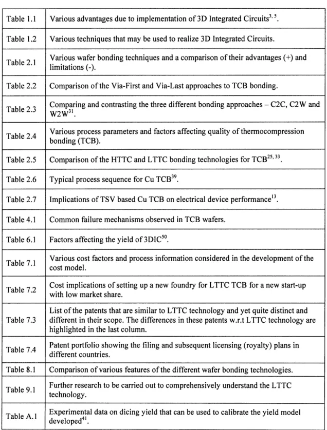
Another motivation for research interest in 3DIC is the ability to integrate different heterogeneous device technologies together without making any modifications to the existing optimized processes for each of these technologies. Heterogeneous integration of devices4 can be used to realize optoelectronic integrated circuits (OEICs) and System-on-Chip (SoC) architectures with adequate reliability as illustrated in Fig 1.1.
Wafmer
3-D Chip
Fig 1.1: Heterogeneous integration of devices on a 3D IC layout platform to make SoC4.
1.2 ADVANTAGES OF 3D INTEGRATED CIRCUITS
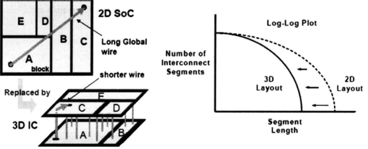
The advent of 3D integration offers many advantages compared to the conventional 2D platforms for device fabrication that was adopted in the past. Table 1.1 lists out the various advantages of a 3DIC platform3' 5. Fig 1.2 illustrates the reduced average distance between transistors due to the 3DIC architecture that helps enhance circuit speed and frequency of operation5. The logarithmic reduction in the number of interconnect segments for all lengths of interconnects is revealed by the graph6
Table 1.1: Various advantages due to implementation of 3D Integrated Circuits3' 5
ADVANTAGES of 3DIC
* Heterogeneous integration of devices to realize OEIC and SoC. * Reduced distance of global interconnects -- Enhanced speed. * Higher integration density -+ more portable devices.
* Higher form factor (capacity / volume ratio).
* Cheaper than further downscaling beyond lithographic limits. * Faster access between memory and logic device modules.
* Reduced overall resistance -- lower joule heating and heat dissipation. * Reduced packaging cost.
*
Reduced power -+ fewer I/O pins to be driven. * Higher fault resistance.1.3 APPROACHES TO 3D INTEGRATION
There are various approaches to realizing 3D integration. Each of these approaches has their own advantages and limitations. These have been highlighted in Table 1.27,
8, 9, 10, 11, 12 below. Based on the analysis presented in Table 1.2, the motivation for use of wafer bonding as a technique to 3D integration is clearly evident as it enables integration with a high density of interconnection and
does not disturb the existing optimized process technology sequence used for each of the individual wafers. Fig 1.3 illustrates the various wafer bonding techniques"3 mentioned in Table 1.2. Number of Interconnect Segments Segment Length
Fig 1.2: Reduction of global interconnect length and density of interconnects for 3D IC layout' 6. Table 1.2: Various techniques that may be used to realize 3D Integrated Circuits.
Technique Advantages / Limitations
K BEAM RECRYSTALLIZATION7'8 (-) High temperature during melting of polysilicon
(recrystallization) - cannot be sustained by 3D devices7' 8.
Deposition of a second level polysilicon layer on top of an oxidized Si wafer in order to fabricate Si
based thin film transistors on it. Need for intense (-) Lack of con deposited, lower grain size variations in electron or laser beam to induce recrystallization compared to single crystal silicon, effects of compared to single crystal silicon, effects of and remove grain boundaries in polysilicon. unintentional doping.
1 SILICON EPITAXIAL GROWTH9 (-) High temperature of epitaxy growth (10000
C) Etch a hole through a passivated Si wafer and affects device quality in lower Si device layers9 epitaxially grow single crystal Si through the
etched hole using the whole base Si as the seed (-) Not suitable when metallization layers present layer. Si epitaxy involves vertical growth of Si under the dielectric since T = 10000C can cause Al layer. Si epitaxy involves vertical growth of Si metal lines to melt and Cu to substantially self-through the etched hole followed by lateral diffuse9.
1 SOLID PHASE CRYSTALLIZATION'o' , (+) Localized crystallization, low thermal budget (500 - 6000C)'.
Low temperature growth of amorphous silicon on (+) Lateral crystallization, dopant activation, oxidized Si substrate and subsequent lLateral crystallization, dopant activation, crystallization induced on the amorphous Si layer even when metallization layers are present 11
to form polysilicon using Ge seeding or Ni metal
catalysts. (-) Slow process.
5 PACKAGE LEVEL 3D INTEGRATION'2
(+) Simple & high yield process.
Vertical stacking of dies or packaged chips using Low density of interconnection. Wires could
(-) Low density of interconnection. Wires could
wire bonding or solder balls as interconnects to short each other in a large MCM.short each other in a large MCM. make multi-chip modules (MCM).
(+) Optimized processes for individual wafers
B WAFER BONDING remain undisturbed.
Fabricate devices and interconnects on individual (+) Higher density of interconnection. wafers and physically bond them after each wafer
has been fully processed vertically for any level of (-) Issues of bond adhesion quality due to thermal
stacking. induced strain, patterned wafer alignment issues,
wafer bowing and warping.
+ Seoding
, G#AnOowth
.. 14.. l l l lI,
to d
Fig 1.3: Various bonding techniques for 3D integration - (a) Beam recrystallization, (b) & (c) Solid phase crystallization, (d) Processed wafer bonding. 13
~4. - ~' !3430 ple
6--il
\ w*wv ATA IUMAf* &ýCHAPTER 2
2. COPPER THERMOCOMPRESSION BONDING - OVERVIEW
2.1 TECHNIQUES OF WAFER BONDING
In order to stack wafers vertically on top of each other and bond them vertically, various bonding techniques have been explored in the past. Some of the more prominent techniques are listed in Table 2.1 along with a critical assessment of their advantages and limitations. Based on the analysis in Table 2.1, it is evident that thermocompression bonding (TCB) could be a good technique to adopt since the bonding metal layer serves the dual purpose of a mechanical as well as an electrical contact. In the other bonding techniques, further processing would be required for electrical interconnection thereby making the process more complex and reducing the yield.
Table 2.1: Various wafer bonding techniques and comparison of advantages (+) and limitations (-).
5 DIRECT BONDING
Bonding (fusion) of two contacting wafer surfaces at room temperature without any intermediate layer. Materials bonded: Si-Si'4, Si-SiO215. Formation of van der Waals or hydrogen bonds.
Subsequent bond strengthening by annealing at elevated temperatures.
Surface activation bonding (SAB)16 - oxygen plasma pre-treatment for wafers before bonding + RCA wet clean to enhance bond quality.
(-) High annealing temperatures - (700 - 10000C) -cannot be sustained by metallization layers. Thermal expansion coefficient mismatch induced residual stresses5.
(-) High annealing temperature may need to be
compromised with ultra-high vacuum (UHV) levels and bonding duration -+ lower bonding throughput.
(-) SAB increase surface roughness17 degrading
bond quality. High sensitivity to wafer bow, warpage and patterns. Bond only serves as a mechanical contact.
(+) Best alignment accuracy among all bonding methods (since bonding done at room temperature)1S.
R SOLDER I/ EUTECTIC BONDING"9 Use of a low melting temperature temperature) alloy as an intermediate facilitate bonding between wafers.
(eutectic layer to
Eutectic alloys used - Au-Si, Au-Ge, Au-Sn.
* ANODIC BONDING21'22
Application of an electric field (100 - 1000V) between an insulating substrate (e.g. glass) and conducting substrate to enhance bonding strength through electrostatic attraction.
Materials - Silicon / metals with glass at
T = 300 -4000C.
I THERMOCOMPRESSION BONDING
Traditionally refers to application of an external high pressure load and high temperature in order to bond the wafers by plastic deformation.
Materials - Si24, glass, eutectic, Cu2 5, Au26.
(+) Low temperature process (280 - 3600C). Less sensitive to surface roughness, topology and particulates20.
(+) Conductive eutectic alloys serve as mechanical and electrical contact for the bonded wafers. (-) Eutectic material may experience dewetting close to the eutectic temperature leading to low bond adhesion. Voids / non-uniformity at the bonding interface 9.
(-) Spontaneous oxide formation of Sn, Ge or Si under ambient condition hinders bonding 9.
(+) Less sensitive to surface roughness and particulates2 1
'
22(-) Thermal expansion coefficient mismatch induced residual stresses. Outgassing of glass at room temperature23
(+) High temperature requirement may be relaxed through high applied load and plasma activation. Bond serves electrical and mechanical contact2. (+) For metallic TCB, high thermal conductivity of metals compared to polymers or oxides makes it a thermal conduit ensuring effective release of heat from joule heating25.
(-) Thermal expansion coefficient mismatch induced residual stresses. Oxidation of bonding surfaces impedes good bond quality. Highly sensitive to surface cleanliness and roughness25.
I ADHESIVE BONDING
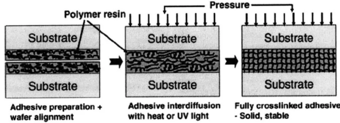
Use of a polymer adhesive on one or both wafer surfaces and application of pressure to enforce wafer contact through the intermediate adhesive layer (Fig 2.1)27.
Adhesive Material - Benzocyclobutene (BCB).
(+) Relatively low bonding temperature. Insensitive to the topology and surface contaminants on the wafer surface. Compatibility with standard CMOS process. Any two materials may be bonded28. (+) Simple, robust & low-cost process. No CMP, surface activation or wafer cleaning needed28 (-) Temperature instability of polymer (need for high glass transition temperature), mechanical instability, Outgassing of polymer during bonding could cause void formation. Low creep resistance and high moisture uptake27
I Pressre
Polymerreain I I I II I I I I I I II
Adhesive preparation + water alignment
Adhesive interdiffusion Fully crosslinked adhesive with heat or UV light -Sold, stable
Fig 2.1: Adhesive bonding process using polymers such as BCB as intermediate glue layer27
2.2 BONDING ARCHITECTURE
Various architectural aspects may be explored in the process of wafer bonding and stacking. They differ in the sequence of processes used (via-first / via-last)29 or the sequence of the interfaces being bonded (face-to-face [F2F] - back-to-back [B2B] / face-to-back [F2B])30 or the elemental blocks involved in the bonding (chip-to-chip [C2C], chip-to-wafer [C2W] and wafer-to-wafer
[W2W])31. Let us explore each of these in greater detail.
2.2.1 VIA-FIRST & VIA-LAST PROCESS
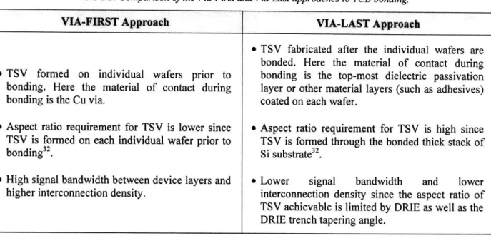
In the process of bonding 3D devices, the through-silicon via (TSV) via interconnecting the metallization layers of different wafers could be fabricated in two sequences. One sequence is where the via could be formed before bonding so that the TSV are bonded upon wafer contact. This is called the VIA-FIRST approach29. The other sequence is where the dielectric passivation layers of the wafers are bonded together and this is followed by etching high aspect ratio holes to form TSV and interconnect the device layers of the various wafers. This is called the VIA-LAST
"111\
34
approach29
. Table 2.2 provides a brief comparison of these two approaches of TSV fabrication29, 32. Based on the various wafer bonding techniques described in Table 2.1, direct, anodic, eutectic and adhesive bonding are all compatible only with the via-last approach where the bonding is initiated between any two material interfaces and through-silicon via interconnections formed after the bonding process. Metal thermocompression bonding is however compatible for both via-first and via-last approaches.
Table 2.2: Comparison of the Via-First and Via-Last approaches to TCB bonding.
VIA-FIRST Approach
* TSV formed on individual wafers prior to bonding. Here the material of contact during bonding is the Cu via.
* Aspect ratio requirement for TSV is lower since TSV is formed on each individual wafer prior to bonding32.
* High signal bandwidth between device layers and higher interconnection density.
VIA-LAST Approach
* TSV fabricated after the individual wafers are bonded. Here the material of contact during bonding is the top-most dielectric passivation layer or other material layers (such as adhesives) coated on each wafer.
* Aspect ratio requirement for TSV is high since TSV is formed through the bonded thick stack of Si substrate32
* Lower signal bandwidth and lower interconnection density since the aspect ratio of TSV achievable is limited by DRIE as well as the DRIE trench tapering angle.
2.2.2 F2F-B2B / F2B-F2B BONDING
The bonding interfaces for stacked wafers could be alternating face-to-face (F2F) and back-to-back (B2B) or consistently face-to-back-to-back (F2B) for every interface as illustrated by Fig 2.2 for the case of copper thermocompression bonding30 where "face" refers to the back-end-of-line (BEOL) metallization layers of a processed wafer while "back" refers to the bulk Si substrate on which front-end device transistors are grown. It has been suggested that it is more favorable to bond wafers in an F2F-B2B configuration as compared to a F2B-F2B configuration since every alternating F2F interface enables a very high density of inter-wafer interconnections3° and every alternating B2B segment may be used to fabricate integrated microchannels33 in the Si substrate regions where through-silicon via (TSV) does not exist to enable efficient device cooling and effective 3D heat extraction through microfluidic flow. If an F2B-F2B configuration is used, then high density of interconnections cannot be achieved between any two bonding interfaces thus limiting the device functionality and performance. All the wafer bonding techniques in Table 2.1 are compatible for both F2F-B2B and F2B-F2B bonding interfaces.
---m a~ - ml a 4m F m through-layer 0 vlas device I s -r * IuY~t
~
)ack-to-back bond RIGH DENSIT" E]rT•JCO]NNUCZON8 (fnl azternative bonding interfacee) JIr •8A fGcelLU-iace bondFig 2.2: TCB achieved either by B2F bonding or alternative F2F-B2B bonding strategies30 2.2.3 C2C - C2W - W2W BONDING
The elemental blocks of a bond could be either a chip or the entire wafer. This brings about three possible combinations of structures - chip-to-chip (C2C), chip-to-wafer (C2W) and wafer-to-wafer (W2W) bonding3 1. The differences between these bonding schemes are highlighted in Table 2.3. Based on the comparison provided, from a mass scale production perspective, where high throughput and yield are both required, W2W bonding seems to be the best approach to bonding and this is indeed the technique adopted by most companies that have developed novel electronic devices using 3D integration since it requires minimal investment in acquirement or modification of existing processing equipments (most standard fabrication equipments in a fab are for wafer-scale processing) for the additional 3D processes. All the bonding techniques in Table 2.1 are compatible for C2C, C2W and W2W stacked structures.
back-to-face bond
back-to-face bond
IIII IIIII II IIIII.LIII 1II-I -IU
'
Table 2.3: Comparing and contrasting the three different bonding approaches - C2C, C2W and W2W 3
C2C Bonding
* Very low throughput. * Traditional manufacturing
and packaging methods such as die attach and wire bonding required.
* More serious reliability concerns in the case of high density wire bonding interconnection as these wire bonds could short each other affecting circuit functionality3 2.
* Highest yield if "known good die (KGD)" are identified and bonded.
C2W Bonding
* Stacking of dies of different sizes such as a 12" logic
device Si wafer with a 4" RF device GaAs wafer -less efficient use of larger wafer.
* Usually lower throughput than W2W bonding. Throughput is very sensitive to the number of chips per wafer.
* Bonding with "known good die (KGD)" ensures higher
overall yield than W2W. * Bonding of multiple dies on
a base wafer - formation of
via after bonding is difficult
- via-first bonding
approach is preferred. * Need to adjust the center of
force while permanently bonding all the chips to the wafer base when some die on the base wafer are not KGD and therefore not bonded to any chip on top. * Limited substrate
back-thinning capability due to presence of non-uniform unbonded vacant sites on base wafer.
* Flexible chip size, reduced design cost, shorter time to market.
* Less stringent alignment requirements than W2W bonding.
W2W Bonding
* Very high throughput as all chips in the wafers are bonded at once. * Increased flexibility of
using existing fab equipment for further processing.
* Need for temporary
bonding of thin wafers with carrier wafers using adhesives to enable wafer thinning prior to bonding. * Chips of each stacking level
need to be of the same size. * Very stringent alignment
requirements; yield is highly sensitive to
alignment. Relatively lower yield process.
2.3 FUNDAMENTALS OF THERMOCOMPRESSION BONDING
Thermocompression bonding (TCB) typically involves bonding of the metal layers on the bonded wafers. There are various process parameters and physical factors that affect the metal-metal bond toughness. All these factors need to be controlled and optimized in order to achieve a good bond quality. The most prominently used material for TCB is copper (Cu) since it is also the material of choice for the current generation of nano-interconnects. Table 2.4 lists out the key factors that influence the bond quality2 5, 33.
From Table 2.4, it is evident that good bonding can be achieved with a high applied load and CMP polished surface along with either a high temperature bonding or with high vacuum condition at low temperature. This argument brings us to two distinct modes of TCB namely high temperature thermocompression (HTTC) and low temperature thermocompression (LTTC). The distinct features of these two bonding approaches is presented next.
Table 2.4: Various process parameters andfactors affecting quality of thermocompression bonding.
PARAMETERS EFFECTS
* High temperature bonding at around 400 - 5000C is typically used for Cu bonding as these high temperatures cause decomposition of CuxO if any formed2 5.
BONDING
TEMPERATURE * Low temperature bonding (<I000C) would be desirable so as to minimize the thermal mismatch induced residual stresses in the fabricated device and
metallization layers33.
ANNEALING * Post-bond annealing at moderate temperatures helps in enhancing grain growth and
TEMPERATURE inter-diffusion and forming a good bond interface25
* To prevent surface re-oxidation of Cu and minimize presence of surface
VACUUM contaminants during the bonding process, an ultra-high vacuum (UHV) level of
LEVEL about 10-10 Torr is desirable. Current wafer bonders however are not equipped with this facility and vacuum levels around 10'5Torr is the current standard33.
MATERIAL GEOMETRY PROCESSING APPLIED PRESSURE BONDING DURATION
* Although Cu is the standard material of choice for TCB, Au may also be an attractive option. Bond quality depends on the yield stress and work hardening index. Since these two material properties are lower for Au as compared to Cu, the true contact area of bonding for Au could be higher than Cu, leading to a low resistance contact although resistivity of Au is higher than Cu25.
* Oxidation of Au is kinetically not very feasible as compared to the spontaneous non self-passivating oxidation process in Cu. Oxide coated metal bonding leads to very
low bond quality depending on the number of oxide monolayers formed2s5.
* Processing issues associated with Au limit its applicability and it also introduces deep donor trap levels in the forbidden bandgap of Si affecting performance of minority carrier devices.
* Bond quality affected by thickness of bonding metal layers. Thicker layers undergo increased plastic deformation and enhance bond quality3 4.
* Higher surface roughness of wafers is detrimental to a good bond quality. Reduction of surface roughness requires chemical mechanical polishing (CMP)25.
* Smaller pattern feature sizes increase bond strength since load pressure is inversely proportional to the area of the feature.
* Orientation of the features with respect to any crack initiation sites also affects the bond integrity. If crack is oriented perpendicular to the features, then fracture resistance is higher since multiple crack initiation and nucleation events would be necessary for complete bond fracture3 5.
* Bonding surface pattern density and non-uniformity in pattern density across wafer have an effect on bond quality.
* Surface pre-bond cleaning using acetic acid or HCI or RCA and reducing gas (N2 / H2) purge in the bonding chamber to remove any native oxide helps enhance bond toughness. Plasma activation of surface (SAB)'6 improves bond quality.
* Post-bond annealing in order to facilitate grain growth, atomic self-diffusion and recrystallization at the metal bonding interface that helps increase bond toughness25.
* Higher applied pressure enables elastic deformation of bowed wafers and enhances bond quality as a result25.
* Bond duration is an important criterion especially for low temperature bonding where sufficient time is required for grain growth and atomic interdiffusion when the kinetics is unfavorable.
2.3.1 HIGH TEMPERATURE THERMOCOMPRESSION (HTTC)
High temperature thermocompression (HTTC) bonding involves bonding of metal coated wafers at relatively high temperatures of around 400 - 5000C at moderate vacuum levels of about 10-5
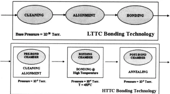
Torr2 5. The high temperature causes the metal layer to have a low yield stress and undergo substantial plastic deformation to form a good interface and strong metallic bond under a moderate to high applied load. A typical scheme for HTTC could be to have a pre-bond chamber for wafer cleaning and alignment at a very low vacuum of 10-3 Torr, followed by a high vacuum bonding chamber at 10-6
Torr and subsequently a post-bond annealing chamber also at a low vacuum of 10-3 Torr as illustrated in Fig 2.3. This kind of a scheme is currently being
implemented by Tezzaron® and EV Group® 36.
There are various problems associated with the HTTC process. The large thermal expansion coefficient mismatch induces differential expansion of various material layers in the processed device wafers causing high residual stresses to be developed that could cause the wafers to bow or warp. This could degrade the performance characteristics of the fabricated devices. Therefore, use of high temperature is to be avoided.
2.3.2 LOW TEMPERATURE THERMOCOMPRESSION (LTTC)
The problems associated with the use of a high temperature may be resolved by using a low temperature (possibly room temperature) process. However, at low temperatures, since oxide decomposition is unfavorable, other suitable measures need to be taken that include use of UHV to avoid an oxidizing ambient as far as possible and in-situ pre-bond cleaning of the wafer surface using acetic acid and reducing gas purge (H2 / N2) as well as plasma activation for enhancement of bonding33. As indicated in Fig 2.3, the vacuum levels needed for LTTC could be as high as
10-10 Torr33. All the bonding processes including cleaning and alignment are performed at 10-10
Torr without any break in the vacuum. The use of LTTC has not been adopted in the industry yet and it is a topic of current research at various research institutions and universities, including
I . - 1
Fig 2.3: Typical bonding process sequence for HTTC and LTTC bonding technology.
2.3.3 ISSUES WITH LTTC TECHNOLOGY
The commercializing potential of the LTTC technology depends on the yield and throughput of this new process as well as the additional costs involved in using UHV vacuum pumps and chambers to maintain the bonding chambers at 10"10 Torr. Moreover, the yield and throughput of this new technology remains a major issue of concern. Unlike the HTTC process where the high temperature enables good and fast bonding due to favorable kinetics that facilitates grain growth and diffusion, the LTTC process is not thermally activated and therefore a longer bonding duration would be required for good adhesion to be achieved although recrystallization of copper can take place even at room temperature since Cu has an intrinsic high grain boundary mobility at room temperature37
. This in turn translates to a lower throughput for LTTC thus requiring more LTTC bond chambers and vacuum pumps to cater to the production rate in the industry. All these concerns are addressed in a later chapter which presents a cost model comparing the LTTC and HTTC technologies from an economic perspective. Table 2.5 summarizes some of the key differences between the HTTC and LTTC technologies described above.
Bause
Pssurn= ID Torr.
LTTC Bonding Technology
PREBOND
CLEANING ALIGNMENT
Pr• -' To3Test. Presma -W Tart. Prssmm 2 Ternr.
T o Thnlo HTTC Bonding Technology !
-- I I
t fTable 2.5: Comparison of the HTTC and LTTC bonding technologies for TCB2 5' 33
HTTC Bonding
LTTC Bonding
* Bonding temperature - 400 - 5000C --+ favorable *Bonding temperature < 1000C (or room
kinetics for good bonding in a shorter duration as temperature) -- kinetics not very favorable for copper oxide decomposition is favored at these bonding. Longer duration needed to achieve good high temperatures. Higher throughput. adhesion. Lower throughput.
* Higher thermal expansion coefficient mismatch * Minimal thermal induced stresses. Device induced residual stresses. Device performance performance unaffected3 3.
affected3 3.
* UHV vacuum of 10-10 Torr required. Surface * Lower vacuum levels needed. Surface activation activation or plasma treatment may be helpful33.
or plasma treatment may not be required.
* Yield is highly sensitive to the vacuum level * Yield is affected by the high CTE mismatch achieved and bond duration.
induced residual stresses.
* Need for UHV systems incurs extra expenditure. * Already commercialized38. Still in research phase.
2.3.4 PROCESS SEQUENCE FOR TCB
There are various processing steps needed to realize Cu TCB. After the wafers have been fully processed including front-end-of-line (FEOL) as well as back-end-of-line (BEOL) (devices and interconnects fabricated) using their corresponding sequence of processes, Cu leads that protrude out of the wafer surface need to be fabricated. This involves a sequence of additional process steps as listed in Table 2.639. This is just one of the possible process flows that could be considered. Other process sequences may also be acceptable. It is necessary to ensure during these process steps that the temperature is kept low to avoid affecting the device performance.
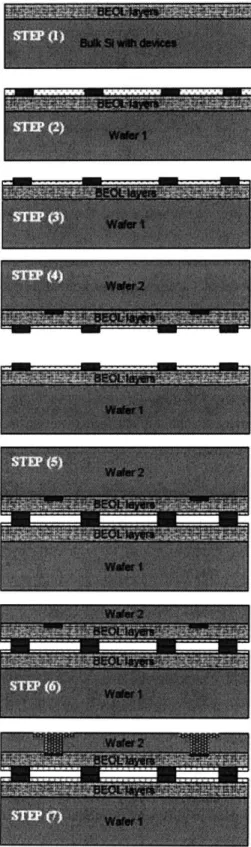
Fig 2.4 shows a schematic of the process sequence used for a two-wafer F2F bonding where the passivating oxide layer is recessed to expose the Cu patterns on the bonding surfaces40.
Table 2.6: Typical process sequence for Cu TCB3 9.
PROCESS SEQUENCE for TCB
1. LITHOGRAPHY - The regions on the processed passivated wafer surface where etching is to be carried out for deposition of through-silicon via (TSV) needs to be defined.
2. DRIE ETCHING - The standard DRIE BOSCH® process (SF6 / CF4 chemistry) which is used in MEMS processing is to be used here for etching high aspect ratio (AR) holes or trenches for TSV via.
3. COPPER SEED LAYER DEPOSITION - A seed layer of Cu is to be deposited at the high AR
trench bottom to enable subsequent electroplating of Cu to fill the TSV trench.
4. COPPER ELECTRODEPOSITION - Having etched the TSV holes, blanket electrodeposition of
copper is performed to form Cu filled TSV and additional Cu blanket films on the surface of the wafer.
5. CHEMICAL MECHANICAL PLANARIZATION (CMP) - A CMP process is used to flatten the
wafer surface prior to bonding and polish away the extra Cu films on the wafer surface.
6. OXIDE ETCH - Etch away a small layer of inter-metal dielectric (IMD) on the surface of the wafer to cause the TSV Cu leads to protrude.
7. WAFER CLEANING - Use RCA or acetic acid solution to clean the wafer and strip out any intrinsic metal oxide layers formed.
8. SURFACE ACTIVATION - Use 02 or Ar plasma to activate the surface prior to bonding. This step is however optional.
9. ALIGNMENT - Ensure precise alignment of the wafers with minimal alignment errors.
10. BONDING - Bring the wafers into contact and apply sufficient load to so as to cause plastic
deformation of the contacting metal surfaces and enable metallic bonding to take place.
11. ANNEALING - After bonding, perform a moderate temperature anneal (5000C) to allow for grain growth, Cu interdiffusion and creation of a good adhesion bond interface.
2.3.5 PROCESSING ISSUES IN TCB
There are various processing issues to be considered during the thermocompression bonding process. These issues need to be tackled effectively in order to achieve a high bonding yield and sufficient true contact area of the bond. Some of the key issues are discussed below:
DISHING - In patterned Cu lines to be bonded, the use of CMP for polishing these lines prior to actual bonding could result in "dishing" effects as shown in Fig 2.525. As a result of dishing, the true contact area of patterned wafers that are bonded is very low thus resulting in poor bonding quality. Even large applied loads may not be helpful in minimizing dishing effects much since the depth of these dished pits can be as high as around 50 nm.
Fig 2.4: Typical process sequence for F2F TCB patterned Cu layer bonding - Steps -(1) FEOL + BEOL; (2) oxide layer deposition, patterning and Cu pad formation; (3) oxide layer recess to expose Cu pads; (4) F2F alignment; (5) Thermocompression bonding; (6) CMP to back grind top wafer and (7) lithography and patterning for TSV and probe-pads4 0
Cu Lines
I -- --- :I:: a~n A1.4.AA- il
Fig 2.5: Illustrating the dishing effects observed in patterned Cu lines due to CMP25.
Thefigure on the right is the actual profilometer image used to determine the depth of a Cu dish surface.
GLOBAL BONDING NON-UNIFORMITY - While dishing effects account only for local
bonding non-uniformities for patterned Cu lines, global non-uniformities30 in the bonding area could also exist due to wafer bow and warping induced by the FEOL and BEOL processing of the wafers and insufficient elastic deformation at the edges of the bowed wafers to achieve good contact. These bowing effects are detrimental to bond quality on a global wafer scale. An additional source of global bonding non-uniformity could be the non-uniform density of pattern features and wrong center of gravity for the applied load resulting in non-uniform pressures at different locations of the bonding wafers.
CARRIER WAFERS - The substrate bulk layer of the wafers that are bonded need to be thinned in order to stack more levels of wafers. Substrate thinning and TSV fabrication after bonding could be detrimental to the bond quality and therefore, it is usually carried out before the bonding process. It is difficult to handle thin wafers for bonding as they are brittle and tend to warp or bow easily. Temporary bonding of thin substrates to carrier wafers is a useful approach to enable good bonding.
The sequence followed for temporary bonding and debonding is shown in Fig 2.6"3. The device wafer is first bonded to a carrier wafer using an adhesive layer with the device layer face down in contact with the adhesive layer. This is followed by wafer thinning and subsequent bonding of the carrier supported thinned wafer with another wafer. Finally, after bonding, when the carrier support is no longer required, appropriate temperature or UV light or chemical solutions are used to detach the carrier wafer finally resulting in a successful thinned wafer bonding.
Cu Lines · i i I:..· I · 1-r i i ; r
Devce' Water Front End Processing
(Lithography. etching, etc.)
Dev~ce Wafer
Release Layer Carrier Wafer
Temprry ondirng
Device Water bonded
on CArrim Wafer
Back Thinning and further Processing
oevCko Wafer (thirrl n Carrier Water
I
Dewes waier Oevice Wafer thLine
on Carrier Wafer PermanentWater Bonding 3D lntegraon vi Lar 'flarWer Debondnig Packaging
Fig 2.6: Process sequence for wafer bonding involving use of carrier wafer to handle thin substrates3 .
WAFER ALIGNMENT - For sub-micron high density pattern features to be bonded, the
alignment of the wafers prior to and during the bonding period needs to be very precise. However, there are limits to the accuracy achievable in alignment. There are two methods of alignment - direct and indirect. Direct alignment involves direct live IR imaging of alignment keys on the wafer prior to bonding while indirect alignment involves the use of an external reference positioning system.
Devices with low interconnection density can tolerate alignment errors around 2 pm while in the case of high interconnect density, alignment accuracy in the sub-micron range would be required31. Alignment errors could arise either prior to bonding during the alignment phase due to the performance limitation of the aligning equipment or during bonding due to temperature and pressure non-uniformity that could cause bowing or warping and increase misalignment errors. Statistical process control (SPC)31 is required in order to minimize alignment errors as far as possible.
2.3.6 ELECTRONIC IMPLICATIONS OF TCB
It is necessary to examine the effects of wafer bonding on the electrical device and circuit performance parameters. Some of the electronic implications of TCB based wafer bonding are
I
discussed in Table 2.7". Although not specific to TCB, in general, all wafer bonding based 3D integration schemes have similar implications on the electrical device performance characteristics.
Table 2.7. Implications of TSV based Cu TCB on electrical device performance13.
IMPLICATIONS OF TCB on ELECTRICAL DEVICE PERFORMANCE
1. POWER - 3D integration results in a smaller wire length distribution as compared to 2D with the largest reduction observed for the longest paths. Shorter wires imply lower average load resistance and capacitance and decrease the number of repeaters needed for long wires thereby causing less power loss. Compared to 2D, 3D ICs are expected to improve the wire efficiency by 15% and reduce total active power by more than 10%.
2. NOISE - Shorter wires in 3D have lower wire-to-wire capacitance resulting in less noise coupling between signal lines. Reduced number of repeaters also ensures lower noise and higher signal integrity. Moreover, electromagnetic interferences such as interconnect crosstalk, wire-substrate coupling and inductance effects are much lower in the case of 3D IC.
3. FAN-OUT - Since 3D ICs have a lower wiring load, a greater number of logic gates may be driven implying higher fan-out.
4. INTERCONNECTS - As interconnects (Cu) in the 2D circuits are further downscaled and the barrier layer thickness (Ta) unable to be proportionately downscaled, surface scattering effects of electrons become dominant in addition to the electron bulk scattering mechanisms such as phonon scattering. This increases the effective resistivity of Cu nano-interconnects significantly thereby motivating the need for 3D ICs so that further downscaling of interconnects can be avoided and yet performance improvement achieved due to lower total global interconnect length in a 3DIC. Increases in interconnect temperature due to joule heating effects also cause the resistivity of Cu to increase. Avoiding further downscaling in 2D by moving to a 3D layout prevents further aggravation of joule heating.
5. INDUCTANCE - Reduction of wire length helps reduce inductance and presence of second substrate close to the global wires might also help lower the inductance by providing shorter current return paths provided the substrate resistance is sufficiently low.
CHAPTER 3
3. PHYSICS & MECHANICS OF WAFER BONDING
3.1 PHYSICS & MECHANICS OF WAFER BONDING
Having looked at wafer bonding and its classifications, techniques, associated process sequence, process and material issues, failure mechanisms and its effects on the electrical device performance, it is necessary to take a physical perspective and analyze the bond strength of bonded wafers with respect to various factors that would impact it. This requires development of a mechanics-based model to quantify bond strength. This chapter presents the model developed to characterize the bond strength of bonded wafers.
Wafer bonding is accomplished by bringing the wafers into contact with each other so that chemical bonds could be formed at the interface. Since the forces of attraction are short range, sufficient load is to be applied to bring the rough (non-flat) surfaces into contact. Since the wafers are typically bowed as illustrated by Fig 3.1, we can model the bonding process such that the wafers come into contact at the centre and then the applied load causes elastic deformation of the wafers and the bond front propagates from the centre towards the edge34. As the bonds are formed, the surface energy is lost and interface energy is gained. In addition, elastic energy is also stored when bowed wafers are bent for bonding to be initiated.
'Taking the surface energy for wafers I and 2 to be yj and y2 and the interfacial energy to be Y12, the net change of energy due to the formation of the bonded interface is known as Dupre work of
adhesion (W) and is expressed as in (2). This work of adhesion refers to the energy available per
unit area to bond two surfaces. The requirement for a successful bonding to take place is that the work of adhesion must be sufficient to cause the wafers to deform elastically to a common shape.
W = Y1 7 Y2 - Y12 (1)
Given that the two wafers being bonded each have a width (B), the total energy in the system, UT as a function of bond front position, a, is given by (2) where the first term, UE is the elastic energy accumulated in the wafers as they conform to one another and is a function of the bond front position. The second and third terms refer to the total interface and surface energies of the bonded and unbonded regions of the bond face respectively34.
The system attains equilibrium when the total system energy is minimized. Therefore, the bond front would propagate until the equilibrium condition in (3) is satisfied, where A is the area of the bonding interface when wafer bonding is considered in 3-D.
dUT
o -
w
dUE
da
dA
(3)As long as the inequality condition in (3) is satisfied, the bond front of the bonding interface will continue to progress from the centre towards the edge of the wafer. The quantity dUE/dA refers to the strain energy accumulation rate and it is a function of the wafer geometry and the material
properties. V Separ, (a)
BOND FRONT:
B B4,'tion
sion
ation(a) A typical force separation curve for two surfaces. The area under the curve represents the work of adhesion. (b) The change in system energy as two surfaces are bonded. Surface energy (YI ,72) is lost, interface energy (712) and strami energy (UE) are gained as a increases..
Fig 3. 1: Force-separation curve for two wafer surfaces and illustration of the bondfront for bonding of bowed wafers34
Surface imperfections in the wafer will affect the quality of the bond adhesion and these imperfections may be categorized into three types - (a) wafer bow at the global wafer scale due to residual stresses that arise upon thin film deposition; (b) surface waviness (warping) at the
2Yl
a
--[
millimeter scale and (c) surface roughness at the nanometer scale. Let us first analyze the effect of wafer bow on the bonding success.
3.1.1 EFFECT OF WAFER BOW
3 4Fig 3.2 shows the case of two bowed wafers with initial curvatures, KA and KB, thicknesses hA and hB, elastic moduli EA and EB and a common Poisson ratio (u) where the bond front has propagated up to r = a and another length of (b-a) remains to be bonded. Given this bonding situation, the strain energy, UEi for each wafer may be modeled in terms of the wafer curvature and the other parameters as given by (4) making use of the linear plate theory. In (4), Kf refers to the final wafer curvature after bonding.
U, E, h3.(I_ . iv,).[b2(l+v,)+a2(l(v,)
(4)
Using (5) where the total nominal bonding area A = na2 and summing up the strain energy accumulation rates for both the wafers being bonded, the overall strain energy accumulation rate may be given by (6) where UE = UE1 + UE2. This parameter dUE/dA may now be compared with the work of adhesion (W) to determine the extent to which the bowed wafer surfaces would bond and how successful the bonding would be.
dUE _ dUEl da
dA da dA
dUE
-1
EAEBh,
hB 2 (1+v) 1= -
63.(
-CB
2)2(6)
dA 6 hB+Eh A BE, (1 -v) [(1 + v)+R2(v
Note from Eq. (4) that the strain energy, UE, scales as the bond front propagates. The effect of wafer bow (curvature) on the extent of bonding may be determined from (6) and by comparing it with (1).
3.1.2 EFFECT OF PATTERNING
34In most cases, the Cu films on the wafers to be bonded by TCB are not blanket wafers. Instead, they consist of patterned Cu lines that protrude out from the processed wafers. When bonding patterned lines, since the nominal surface area of contact is now only a fraction of the overall wafer surface area, the energy available to deform the wafers elastically is reduced. As a result, successful bonding becomes more difficult to achieve. Given that the fraction of patterned wafer area in contact during bonding is pa, then using (5), the modified expression for dUE/dA is given