HAL Id: hal-02107973
https://hal.archives-ouvertes.fr/hal-02107973
Submitted on 23 Apr 2019HAL is a multi-disciplinary open access archive for the deposit and dissemination of sci-entific research documents, whether they are pub-lished or not. The documents may come from teaching and research institutions in France or abroad, or from public or private research centers.
L’archive ouverte pluridisciplinaire HAL, est destinée au dépôt et à la diffusion de documents scientifiques de niveau recherche, publiés ou non, émanant des établissements d’enseignement et de recherche français ou étrangers, des laboratoires publics ou privés.
A Universal Approach toward Light-Responsive
Two-Dimensional Electronics: Chemically Tailored
Hybrid van der Waals Heterostructures
Yuda Zhao, Simone Bertolazzi, Paolo Samorì
To cite this version:
Yuda Zhao, Simone Bertolazzi, Paolo Samorì. A Universal Approach toward Light-Responsive Two-Dimensional Electronics: Chemically Tailored Hybrid van der Waals Heterostructures. ACS Nano, American Chemical Society, 2019, 13 (4), pp.4814-4825. �10.1021/acsnano.9b01716�. �hal-02107973�
A Universal Approach towards Light-Responsive
Two-Dimensional Electronics: Chemically Tailored
Hybrid van der Waals Heterostructures
Yuda Zhao1, Simone Bertolazzi1,Paolo Samorì1*
1 University of Strasbourg, CNRS, ISIS UMR 7006, 8 allée Gaspard Monge, F-67000
Strasbourg, France KEYWORDS
two-dimensional materials, photochromic molecules, dielectric, optoelectronic devices, diode
ABSTRACT
Stimuli responsive hybrid van der Waals heterostructures (vdWHs), composed of organic molecular switches superimposed on inorganic 2D materials (2DMs), can combine the outstanding physical properties of the latter components with the virtually-infinite variety of tunable functionality of molecules, thereby offering an efficient protocol for the development of high-performance multifunctional materials and devices. The use of light as remote control to modulate the properties of semiconducting 2DMs when interfaced with photochromic molecules, suffers
and the finite thermal stability of the photochromic molecule in its different states. Here we have devised a universal approach towards the fabrication of optically switchable electronic devices comprising a few nanometer thick azobenzene (AZO) layer physisorbed on 2D semiconductors supported on trap-free polymer dielectric. The joint effect of the improved 2D/dielectric interface, the molecule’s light-modulated dipolar doping, and the high thermal stability of cis-AZO offers highest control over the reversible and efficient charge carrier tuning in 2D semiconductors with a preserved high performance in 2D FET, as quantified in terms of carrier mobility and Ion/Ioff
ratio. The device has the potential to operate as optical memory with 4 current levels and long retention time (>15 hours). Furthermore, by using CMOS-compatible micropatterning process, the photoswitchable resistor-diode transition has been achieved on hybrid lateral heterojunction devices. Our approach is of general applicability towards the generation of high-performance hybrid vdWHs for the emergence of functional and responsive devices.
The physical superposition of dissimilar two-dimensional materials (2DMs), which are free of dangling-bond on their surfaces, offers numerous solutions towards the development of van der Waals heterostructures (vdWHs) with unusual properties and functions.1-5 Alongside 2D-2D
vdWHs, the tailoring of hybrid organic/inorganic vdWHs provides another feasible way for nanoscale material integration by also offering the possibility to introduce the desired functionality through the molecular design.6, 7 Molecules can by design be capable of responding to external
stimuli: they can change their state, even in a reversible manner, when subjected to external inputs like photons, magnetic fields, pH changes, etc.8 In such a way, they can controllably switch
moment, energy level, electron affinity). Among them, photochromic molecules are widely studied compounds, which can respond to light-stimuli at specific wavelengths.9, 10 Due to their extremely
high surface to volume ratio, the atomically-thin 2DMs are very sensitive to the influence of the surrounding environment (for both the top and bottom surface of 2DMs), and their properties (such as, photoluminescence (PL) and electronic charge transport) can thereof be easily modified by external inputs.11-14 The photochromic molecules can directly interact with 2DMs by modulating
their properties (including band alignment and charge-carrier concentration) as a response to light stimuli. Since their interaction is ruled by weak forces thus determining a weak coupling, the hybrid vdWHs, consisting of 2DMs and molecular switches, can retain the impressive electrical characteristics of 2D crystals and enrich the advanced functionality provided by the switchable molecules. Therefore, the combination of 2DMs with molecular systems represents a viable protocol to develop multifunctional hybrid materials and devices suitable for advanced logic, memory and sensing applications.15, 16
Previous work was mostly focused on the hybrid system based on graphene (or reduced graphene oxide) and photochromic molecules.17-19 However, due to the lack of bandgap in graphene, the
prospects for its electronic application remain problematic. To the best of our knowledge, only a few reports have been published on hybrid vdWHs based on 2D semiconductors and photochromics,20, 21 especially for the applications in the light-tunable field effect transistors
(FETs) and p-n diodes. This is because the existence of persistent photoconductivity (PPC) effect after light irradiation in 2D FETs greatly prolongs the device response time and even hinders the observation of the reversible doping effect brought into play by the physisorbed molecules.22, 23
Alongside, some molecules require long irradiation time to undergo isomerization and display a modest thermal stability.24 Such characteristics makes hybrid vdWHs based on 2D semiconductors
and photochromic molecules not suitable for responsive devices. It is therefore essential to develop a universal approach to suppress the PPC effect and modulate via light stimuli the carrier concentration of 2D layers in a controllable manner, with the ultimate goal of realizing the 2D multiresponsive thus multifunctional devices.
In this work, we fabricated hybrid vdWHs formed from photochromic molecules (azobenzene, AZO) and 2D semiconductors (MoS2 or black phosphorus (BP)). The AZO/MoS2 hybrid system
shows light-tunable Raman and PL spectra of monolayer MoS2 induced by the switchable doping
from AZO molecules. In order to minimize the influence from PPC effect, a trap-free polymer dielectric has been exploited in the optoelectronic devices. The photoresponse speed of monolayer MoS2 FET on polymer dielectric is 3 times faster than that on SiO2.The light-controlled charge
transport in MoS2 and BP FETs has been realized via reversible photochemical isomerization of
the AZO layers. Through the tuning of the population ratio of trans-/cis-AZO molecules it was possible to set four conductance states in MoS2 FET. Significantly, the retention time for
metastable cis-AZO state exceeds 15 hours, largely surpassing current state of the art in AZO based memory devices (corresponding to about 2.7 hours).25 By taking advantage of the reversible
doping capacity of AZO on ambipolar BP FETs, in combination with standard micropatterning process, we have fabricated BP based lateral heterojunctions to achieve the local control of the doping level in different regions of the channel and realize the light-tunable p-n diodes. These results provide evidence for the huge technological potential possessed by hybrid vdWHs for the emergence of high-performance multifunctional optoelectronic devices including optically-controlled transistors, multi-bit optical memories, and light-tunable diodes.
Photoswitching of the AZO/MoS2 hybrid system. As prototypical light-addressable molecule
for the functionalization of 2D semiconductors we have focused our attention to a commercial alkoxy-substituted AZO molecule, i.e. 4-(decyloxy) azobenzene. Its special design comprises a photoresponsive AZO unit grafted at the end of a long alkoxy side chain, the latter being capable of promoting efficient physisorption on the surface of 2D semiconductors to form functional superlattices.21, 26 Compared with other photochromic molecules, AZO molecules show several
advantages, such as large conformational changes, sizable change in dipole moment, low rate of photobleaching, and robust isomerization. In fact, spiropyran/merocyanine are prone to undergo photodegradation and the equilibrium of isomerization is greatly affected by the solvent type (and related pH).24 The different dipole moment of the AZO in its trans and cis form makes such
molecule a suitable model system to explore the reversible light-modulated doping/undoping of 2DMs when interfaced.17, 27 The electric field generated by molecular dipoles, analogous to that of
an external gate, can modulate the carrier concentration of 2D semiconductors. This dipolar interaction appears being a more universal physical process compared to charge transfer (which requires the band alignment) in diarylethene containing hybrids and devices thereof.28
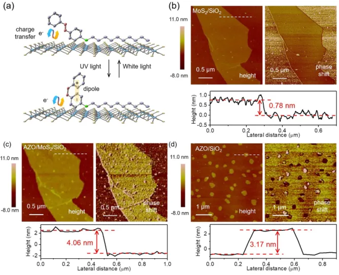
Figure 1a portrays the scheme of the hybrid vdWHs based on photochromic molecules and 2D semiconductor. When exposed to light at specific wavelengths, the AZO molecules can undergo efficient isomerization between different states exhibiting diverse dipole moment. The carrier concentration and even carrier polarity of 2D semiconductors can therefore be directly modulated
via dipolar interactions with the switching photochromic molecules. For 4-(decyloxy) azobenzene
molecules, theoretical calculations also predict that the contribution to the work function (WF) shift of hybrid AZO/2D system from the charge transfer is smaller than that from the dipolar interaction.27 Hence, the dipolar interaction plays the dominant role in the doping of 2D
semiconductors by 4-(decyloxy) azobenzene molecules. The external light stimuli act as the remote control to induce modification in the electronics of the 2D semiconductors, which can be finally read out by monitoring changes detected by optical spectroscopy and electrical measurements. The reversible photoisomerization of AZO molecules on quartz substrates has been demonstrated by UV-Vis absorption, as displayed in Supporting Information Figure S1. In order to characterize the surface morphology of 4-(decyloxy) azobenzene absorbed on monolayer MoS2
we used atomic force microscopy (AFM) in intermittent contact mode. The topographical images of pristine monolayer MoS2 on SiO2 is displayed in Figure 1b. It reveals smooth surface having a
thickness of ~0.78 nm. The AZO molecules are solubilized in ethanol and spin-coated onto the surface of monolayer MoS2. After the deposition of the molecules, the roughness on the MoS2
terraces is enhanced due to the molecular overlayer (Figure 1c). The flake thickness also raises up to ~4.06 nm, indicating a thickness of the 4-(decyloxy) azobenzene layer corresponding to ~3.28 nm. The phase images reveal that the molecules prefer to assemble onto the MoS2 surface rather
than onto SiO2 substrate. The AFM images of AZO molecules on SiO2 (Figure 1d) show random
aggregates with the thickness of ~3.17 nm.
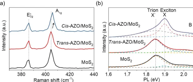
Raman and PL spectroscopy are versatile tools to characterize the correlation between the crystallinity and the electronic structure, enabling also to unravel the effect of various perturbations on the electronics of 2DMs, such as defect, strain and doping.29-31 Therefore, the electronic
interaction between switching molecules and MoS2 can be directly monitored by the spectroscopic
study. Figure 2a shows the Raman spectra of pristine MoS2 and MoS2 with physisorbed
4-(decyloxy) azobenzene molecules (AZO/MoS2). The two main Raman-active phonon modes, A1g
and 𝐸"#$ , can be observed with <20 cm-1 wavenumber difference, which infers the monolayer
slight change of Raman peaks, such as the broadening of A1g peak. After switching molecules from
trans to cis form, we can observe the blue-shift of A1g mode by 1.06 cm-1, the peak sharpening of
A1g mode by 0.64 cm-1 (ΔFWHM) and the almost unchanged 𝐸"#$ mode. The A1g mode is more
sensitive to the carrier doping due to a stronger electron-phonon coupling and the 𝐸"#$ mode is
sensitive to strain due to the symmetry breaking.33, 34 Therefore, cis-AZO molecules induce
p-doping effect on MoS2 and the molecules are physisorbed on MoS2 surface without change of
MoS2 crystal structure. The doping concentration by cis-AZO can be estimated from the A1g peak
shift, which is ~2.3×1012 cm-2.33 Figure 2b shows the PL spectra of pristine MoS2 and AZO/MoS2
hybrid system. The A exciton of monolayer MoS2 consists of both neutral excitons (E(X) ≈ 1.88
eV) and negatively charged excitons (trions, E(X-) ≈ 1.84 eV), so that the trion spectral weight
depends on the amount of doping in the 2D semiconducting sheet.35 Based on the peak fitting
results in Figure 2b, the spectra weight of trion in the pristine sample is higher than that of exciton, due to the n-type doping typically occurring in MoS2 crystals. After the physisorption of
trans-AZO molecules, the weight percentage of the trion peak increases and the exciton peak almost vanishes, demonstrating a slight increase of electron density in MoS2. After irradiation with UV
light, the PL peak blue shifts and the intensity increases. The fitting curves reveal that the trion spectral weight decreases and the neutral exciton peak dominates the spectra. The PL results are consistent with Raman results, demonstrating the depletion of electrons in MoS2 by cis-AZO. After
irradiation with visible light, both the Raman and PL spectra convert back to the trans-AZO/MoS2
condition. By and large, the spectroscopic study provides unambiguous evidence of the efficient light-controlled reversible doping of MoS2 determined by the photoresponsive AZO adlayer. From
another point of view, it also demonstrates the possibility to reversibly control the light emission (wavelength, intensity) of MoS2 monolayer by the AZO molecules.
Improved photoresponse dynamics by using trap-free polymer dielectric. When interfacing
photoswitches with 2D semiconductors and using the hybrid system for light-responsive optoelectronic applications, the presence of the PPC effect represents a major drawback towards the efficient light-triggered device operation.23 The PPC effect has been mainly attributed to the
trap states at the interface and results in a slow (long) response speed (time).22, 36 To achieve fast
response speed and low interfacial trap density, in our optoelectronic devices we opted to use an appropriate hydroxyl-free gate dielectric, i.e. divinyltetramethyldisiloxane-bis(benzocyclobutene) (BCB),37 in order to optimize the 2D/dielectric interface, improve the photoresponse dynamics,
and minimize the PPC effect. Compared with other commonly used trap-free dielectric in 2D electronics, such as poly(methyl methacrylate) (PMMA) and hexagonal boron nitride (h-BN),38, 39
BCB dielectric shows simple and large-scale fabrication process, low processing temperature, high thermal stability, and excellent compatibility with the conventional microfabrication process. Such a thin BCB layer can be deposited on the arbitrary substrate as a universal solution to engineer the dielectric surface. The BCB monomers are spin-coated onto SiO2/Si substrate and annealed to
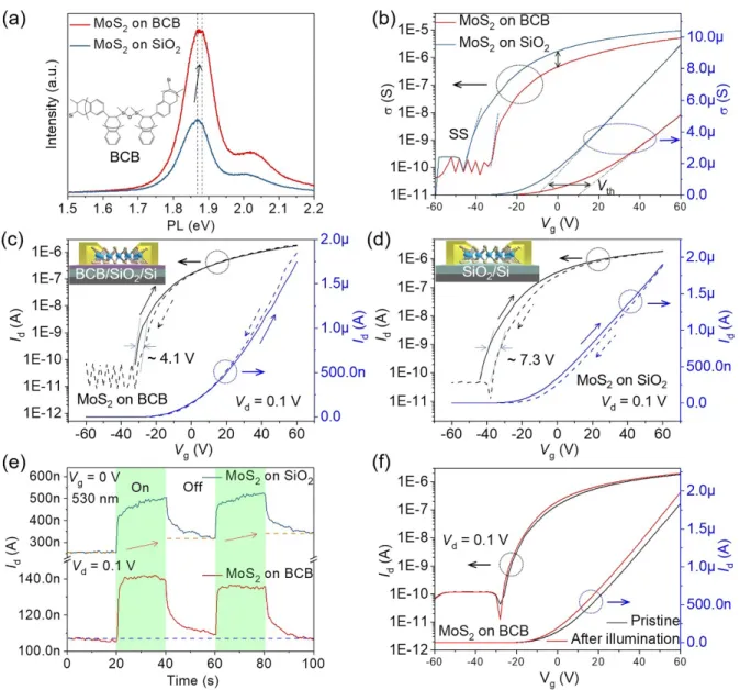
achieve optimal crosslinking (BCB thickness ~60 nm). Figure 3a compares the PL spectra of monolayer MoS2 on BCB and on SiO2 substrate, respectively. When compared with neat SiO2, the
presence of a BCB overlayer determines on the PL of MoS2 both a blue shift and a notable increase
in intensity. The SiO2 dielectric with surface dangling bonds and impurities have been
demonstrated to introduce unintentional n-type doping on MoS2.40 The negatively charged
excitons dominate the PL peak and the high density of interface trap states at SiO2 surface strongly
n-doping effect. The PL peak is dominated by the neutral excitons on BCB, which is similar to the
PL emission of suspended MoS2 flake.41
Back-gated MoS2 FETs were fabricated on both BCB and SiO2 substrate with patterned top Au
electrodes (channel length/width is 0.7 μm/2.4 μm and 0.6 μm/1.2 μm for device on BCB and SiO2
substrate, respectively). Figure 3b shows the 2D conductivity (σ = '(
)(
*
+) of monolayer MoS2 FET
as a function of back-gated voltage (Vg), where Id is the source-drain current, Vd is the source-drain
voltage and L/W is the length/width ratio of the channel. At Vg = 0 V, the conductivity of monolayer
MoS2 on SiO2 substrate is 4 times greater than that on BCB substrate and the threshold voltage Vth
of MoS2 FET on BCB substrate shifts to a more positive value (△Vth ≈ 20 V compared to that on
SiO2 substrate). We can extract the electron concentration (ne) of MoS2 on both substrate, which
is 1.34 × 1012 cm-2 and 0.85 × 1012 cm-2 on SiO2 and on BCB surface, respectively. Significantly,
the electrical transport results on the substrate-induced doping are consistent with those obtained from the spectroscopic measurements. The hysteresis test of MoS2 FET (Figure 3c and 3d, the
value decreases from 7.3 V on SiO2 substrate to 4.1 V on BCB substrate) further demonstrates the
lower trap density at the MoS2/BCB interface (2.86 × 1012 cm-2eV-1) compared to the case of the
MoS2/SiO2 interface (4.69 × 1012 cm-2eV-1).
Due to the high quality of the MoS2 when interfaces with BCB coated SiO2, one great advantage
induced by BCB substrate consists in the enhanced photoresponse dynamics of the MoS2
photodetector and the minimization of PPC effect. Figure 3e shows the time-resolved photoresponse of the MoS2 FET under 530 nm light on both substrates without gate bias. The
device on BCB substrate displays a steep photocurrent rise and decay when switching on and off the illumination. The photocurrent reaches saturation quite fast on BCB substrate, while the
photocurrent continuously increases during the 20 s light illumination on SiO2 substrate. This can
be ascribed to the present of trap states either at the MoS2/SiO2 interface or in the MoS2 itself. The
photo-excited free carriers can be trapped in these states and thereby hindering the recombination of the electron-hole pair. The long-lifetime carriers continuously increase the photocurrent. In addition, the slow relaxation time of the trapped carriers results in the apparent PPC effect of MoS2
FET on SiO2 substrate (Figure 3e, top). We also measure the transfer curves before and after light
illumination (Supporting Information Figure S2). The results show that after illumination, the threshold voltage shifts and the current greatly increases for the MoS2 FET on SiO2 substrate. All
these negative effects will inhibit the observation of switchable doping of MoS2 by photochromic
molecules. In contrast, the time-resolved photoresponse curve (Figure 3e, bottom) and the transfer curve (Figure 3f) of MoS2 FET on BCB coated SiO2 after light illumination demonstrate that the
PPC effect is markedly reduced on BCB. A direct comparison of the response dynamic is displayed in Supporting Information Figure S3. The presence of trap states can dramatically influence the dynamics of the MoS2 photodetector. The rise (τr) and decay (τd) times (defined as the time taken
by the current to change from 10% to 90% of its maximum) of MoS2 device on BCB is 2.60 s and
8.88 s, respectively, which is ~3 times smaller than that on neat SiO2 (9.73 s and 22.04 s,
respectively). Within the time range of the measurement, the current of MoS2 FET on SiO2 is still
larger than pristine level. Therefore, the actual decay time of MoS2 device on SiO2 is longer. The
field-effect mobility of MoS2 on BCB substrate (11.97 cm2V-1s-1) is higher than that on SiO2
substrate (10.30 cm2V-1s-1) due to the suppressed scattering effect.42, 43 By and large, the use of
BCB dielectric represents a powerful method to minimize the PPC effect and improve the photoresponse dynamics for functional devices.
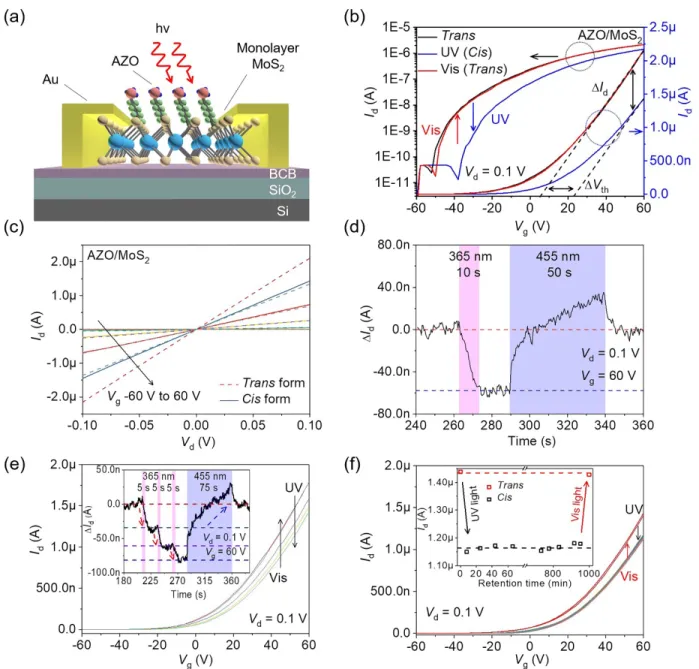
Photoswitchable electrical transport in AZO/MoS2 hybrid devices. After optimization of
MoS2/dielectric interface by employing a thin BCB interlayer, we characterize the switching
behavior of the hybrid AZO/MoS2 FET under light control. The schematic of the device structure
is shown in Figure 4a. The AZO molecules are physically adsorbed on the top surface of MoS2
layer by the same spin-coating process described above and the thickness (~3.3 nm) has been determined by AFM. Compared with MoS2 without molecular adsorption, the trans-AZO
molecules induce n-type doping effect on MoS2 (Figure S4). Figure 4b and 4c display a
representative switching cycle of monolayer MoS2 FET with AZO functionalization. After UV
irradiation, a decrease of drain current in the transfer curves (Figure 4b) can be observed under the whole range of the gate bias and the threshold voltage shifts towards the positive direction (△Vth
= 18.48 V, compared with trans-AZO/MoS2 FET). Therefore, cis-AZO molecules deplete the
electron carriers and induce p-type doping in MoS2. The carrier concentration change induced by
the isomerization of AZO from trans to cis form is ~ 1.11 × 1012 cm-2. The drain current decreases
~34% at Vg = 60 V and a large current ratio (Itrans/Icis≈450) is achieved at Vg = -38 V due to the
shift of the threshold voltage. The determined field-effect electron mobility slightly depends on the state of the AZO: when the latter is in its trans form it amounts to 13.86 cm2V-1s-1 whereas
upon isomerization to cis it decreases down to 10.89 cm2V-1s-1 (~22% reduction). The reverse
process from the low conductance state to the high conductance state can be triggered by visible light irradiation. By doing this, the drain current and the threshold voltage get restored to the original values. Interestingly, the output curves in Figure 4c show a linear relationship under low drain biases (Vd < 0.1 V) regardless of the isomerization of AZO. Such a finding demonstrates a
Figure 4d displays the time evolution of the drain current response for one switching cycle (20-s rest in the dark, 10-s UV light, 20-s rest in the dark, 50-s visible light and 20-s rest in the dark). A current increase and drop can be observed suddenly when the light is turned on and off. It is generally attributed to the generation and relaxation of photoexcited carriers. Under UV irradiation, the current gradually decreases due to the trans-cis isomerization of AZO and under visible light irradiation, the current gradually increases because of the transition back of AZO from
cis to trans form. The rate constants for the trans-cis isomerization can be extracted from the
time-dependent photoresponse curves (Supporting Information Figure S5) and the results are comparable with that in literature.17 Supporting Information Figure S6 shows the photoresponse
of the hybrid device for seven switching cycles. It clearly exhibits two resistance state corresponding to the doping of MoS2 by trans and cis form of AZO molecules, respectively. And
after over 50-cycle switching tests in two months, the device preserved the switching ability with a little deterioration. To rule out potential artifacts, we have performed control experiments on bare MoS2 FET (Supporting Information Figure S7). During irradiation with UV and visible light,
we only observe the photocurrent effect without any gradual current change. Along with the Raman and PL characterizations, we demonstrate that the hybrid AZO/MoS2 FETs show
light-controlled doping effect via the photoisomerization of AZO molecules.
The drain current level can be controlled by the population ratio of trans-/cis-AZO molecules on the MoS2 surface. To trigger the molecular isomerization and adjust the trans/cis ratio we have
used short-time UV light irradiation. The transfer curves reveal gradual current change and continuous threshold voltage shift as portrayed in Figure 4e and Figure S8. The inset in Figure 4e exhibits the time-resolved photoresponse of AZO/MoS2 FET. After each UV irradiation cycle
states can be observed by 3 cycles of UV irradiation and the high conductance state can be recovered by long-time irradiation with visible light. Therefore, the hybrid AZO/MoS2 FET can
retain at multiple current levels by the remote light control. We also characterize the retention behavior of the hybrid AZO/MoS2 FET. The metastable cis-AZO is thermodynamically unstable,
thus it can be switched back to the trans-form by thermal energy. Figure 4f shows the transfer curves of the hybrid devices during the whole retention test. After UV irradiation, the drain current decreases and the threshold voltage shifts to the positive direction, demonstrating the low conductance state due to the p-doping of MoS2 FET by cis-AZO. Then the FET device is kept in
the dark and we record the transfer curves of the FET after different storage time. The drain current and the threshold voltage exhibit very weak fluctuation. After the storage in the dark for more than 15 hours, the device is set back to the high conductance state by visible light irradiation. The inset in Figure 4f plots the drain current at Vg = 60 V with the retention time and it reveals that the
current of the hybrid cis-AZO/MoS2 device is relatively stable (<1% variation) within 15 hours.
In view of its high stability and the multiple current level which can be set by optical stimuli, the hybrid device is promising for the application in optical memory. Regarding the long switching time for photoisomerization of AZO molecules, future study on the improved switching speed will be beneficial for the practical application.
Resistor-diode transition in BP based lateral heterojunction. We have successfully
demonstrated the light-controlled doping of n-type semiconductor MoS2 by the adsorption of AZO
molecules. For the application of 2D semiconductors in electronic components, an ambipolar behavior, i.e. complementary n-type and p-type transistors with the same channel material, is
smart electronics. In this context, it is essential to extend this doping methodology to other 2D semiconductors, especially for p-type or small bandgap semiconductors. Among the 2D semiconductors, few-layer BP FET is well-known for its ambipolar transport behavior with large tunability due to its small bandgap nature.44-46 The precise control of BP’s charge carrier polarity
and carrier density from the molecular approach is desirable for the electronic applications. The few-layer BP FET was fabricated on BCB/SiO2/Si substrate with Cr/Au (3 nm/47 nm) as top metal
contact. The ambipolar transport behavior with dominant p-type transport is observed in pristine BP FET. The detailed characterization and discussion of pristine BP FET can be found in Supporting Information Figure S9.
We first demonstrate the light-controllable doping of BP FET by AZO molecules (device structure shown in Figure 5a, channel length/width is 2.2 μm/3.3 μm). Compared with BP FET without molecules, the adsorption of trans-AZO induces slight p-type doping feature (Figure S10). Figure 5b portrays the transfer curves of the hybrid AZO/BP system for one cycle of light irradiation. As a result of the UV irradiation, the drain current increases at negative gate voltage region and it decreases at positive gate voltage region whereas the threshold voltages for both holes and electrons shift to the positive direction. Such response indicates the p-type doping of few-layer BP flake by cis-AZO molecules. The visible light triggers the back conversion of cis-AZO to trans-AZO. The drain current and the threshold voltage shift back to the previous condition. When the AZO is in its trans form, the field-effect mobility of BP is 32.75 cm2V-1s-1 for the holes and 17.40
cm2V-1s-1 for the electrons, whereas upon isomerization to cis form it amounts to 41.46 and 9.33
cm2V-1s-1 for the holes and electrons, respectively. The doping type of AZO molecules on BP is
the same as that on MoS2. Such result indicates that dipolar interaction is the dominant doping
ratio (Icis/Itrans, ~10 to 102) at 10 V < Vg < 25 V, as displayed in Figure 5c. At 20 V < Vg < 30 V,
BP FET with cis-AZO exhibits hole transport characteristics while BP FET with trans-AZO shows electron transport behavior. The output curves in Figure 5d indicate the formation of good electrical contact for both cis- and trans-AZO/BP FET even under small drain voltage. Overall, light triggered isomerization of the AZO molecules makes it possible to achieve fine and local control of the carrier density and carrier type in BP, being a key step towards the construction of multifunctional devices.
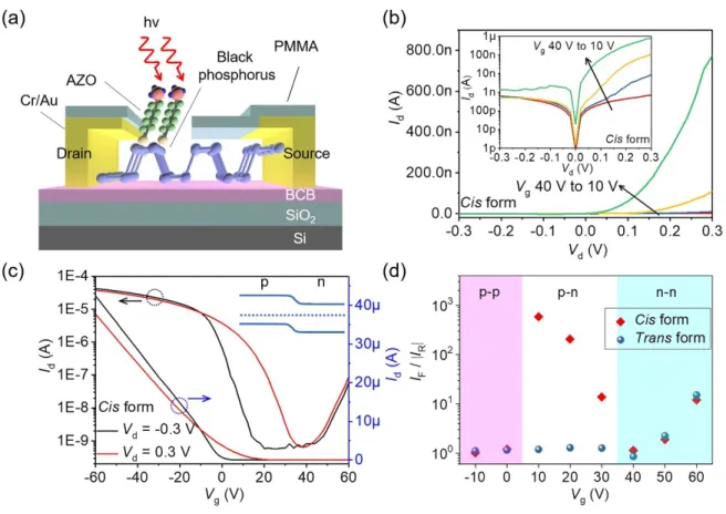
By taking advantage of the capacity of adsorbed AZO to modulate reversibly the electronic properties of BP, in combination with standard micropatterning protocols, we have developed BP based lateral heterojunctions to achieve local control of the doping level in different regions of the channel. This was attained via the selective adsorption of AZO on patterned channel area and by exploiting the light tunable doping ability of AZO. Towards this end, a thin layer of PMMA was patterned by e-beam lithography to partially cover the channel of BP FET and the AZO molecules were adsorbed on the exposed channel area. The scheme of the device architecture is shown in Figure 6a. The junction consists of lateral heterojunction comprising a side-by-side BP and AZO/BP region. Thanks to the ambipolar transport behavior of BP FET, the electrostatic doping by gate can tune the polarity of BP transport. Under certain gate voltage, the pristine BP side switch to n-type transport, while the AZO/BP side remains the p-type transport due to the p-doping effect of cis-AZO. This contributes to the formation of p-n junction in the lateral heterojunction structure. Figure 6b shows the gate-dependent output curves of BP based lateral heterojunction with selective doping by cis-AZO molecules. The inset shows the logarithmic plot of the output curves. We observe the obvious rectifying behavior under Vg from 10 V to 30 V. The rectification ratio, defined
ratio of ~600 is obtained at Vd = ±0.3 V. The minimum ideal factor is 1.82 with Vg = 10 V. The
large ideal factor is related to the Schottky barrier at BP/Cr contract and the BP crystal defects or surface oxidation.47, 48. The current-rectifying effect can also be demonstrated from the transfer
curves at positive and negative drain voltage as shown in Figure 6c. When Vg is in the range of 10
V to 30 V, the drain current shows orders of magnitude difference under positive and negative drain voltage. At negative Vd, the drain current presents a plateau region with minimum current
level, while at positive Vd, the drain current shows normal ambipolar transport behavior. Under
other gate voltage bias, the drain currents display little difference at positive and negative drain voltage. From the band alignment of BP based lateral heterojunction, we can understand the gate-dependent current-rectifying behavior. The Fermi level of BP can be tuned by the back-gate bias and the molecular doping. When the gate voltage is negative, the FET acts as a p-p junction, which shows negligible rectification effect. When the gate voltage exceeds 30 V, the device behaves as
n-n junction and the low drain current is limited by the BP/metal contact and the intrinsic charge
trap. Therefore, in the above gate bias condition, the transfer curves are almost overlapped under positive and negative drain voltage. When the gate voltage is between 10 V and 30 V, the BP side transfer to n-type transport and the cis-AZO/BP side remains p-type transport, which results in the
p-n junction (inset of Figure 6c).
The cis-AZO can convert back to the trans form by the visible light irradiation and the transport behavior of the patterned AZO/BP FET with trans-AZO are shown in Supporting Information Figure S11. The output curves reveal that the current-rectifying effect is quite weak and even disappearing. Figure 6d summarizes the rectification ratio of BP based lateral heterojunction under different molecules state and gate voltage. It reveals that with cis-AZO doping, the hybrid lateral heterojunction device exhibits gate-dependent p-p, p-n, n-n junction transition and dramatic
change of the rectification ratio, while with trans-AZO, the current rectification effect is rather weak. Therefore, the functional devices based on the patterned hybrid AZO/BP FET can switch between diodes and resistors under light control. Such a patterning-based approach was also applied to AZO/MoS2 FETs. The output curves displayed in Supporting Information Figure S12
reveal that the current-rectifying behavior has very weak dependence on the state of the molecules due to the unipolar transport behavior of MoS2. All these results demonstrate that the ambipolar
transport behavior of BP and the p-type doping of cis-AZO molecules synergically contribute to the light-controlled resistors-diode transition on the patterned AZO/BP functional devices. Compared with the previously reported photoswitchable diode based on metal-semiconductor Schottky junction,20 the patterned AZO/BP p-n diode adopts the commonly used FET architecture
and shows the ability of spatially tunable doping, which is ideal for the practical fabrication of functional devices.
Conclusion
In this work, we have demonstrated a universal approach to optically switch 2D electronics by fabricating hybrid vdWHs comprising 2D semiconductors coated with photochromic adlayer, supported on trap-free polymer dielectric. The improved 2D/dielectric interface excludes the unfavorable influence from substrate, thereby minimizing the effect of PPC, and optimizes the device performance, being a prerequisite to the realization of switchable devices. The light-induced geometry change of AZO molecules leads to the redistribution of dipole moment on 2D surface and effectively manipulates the carrier concentration in 2D semiconductors with light as remote control. Both the spectroscopic characterization and the electronic transport measurement
provided unambiguous evidence for the high efficiency in tuning reversibly the doping of 2D semiconductors by light-control over the isomerization of the photochromic molecules. Noteworthy, the achieved modulation over the carrier concentration along with the preserved high FET performance are essential for functional electronic devices, including optical memory and
p-n diodes. The electrop-nic devices based op-n the hybrid vertical vdWHs displayed multiple currep-nt
levels with excellent stability and the switchable resistor-diode transition with spatially tunable doping.
Interface engineering is of vital importance for the electronics of 2D semiconductors, due to their high surface-to-volume ratio. The fine tuning of the interfaces of the 2D materials with both the bottom dielectric substrate surface and the top molecular adlayer enabled us to develop efficient light-responsive vdWHs. Our universal approach offers a guideline for enriching 2D electronics with additional functionalities imparted by ad-hoc molecular switches. The future study on the formation of ordered molecular structures can maximize the collective molecular dipole moment change and extend the carrier modulation range. Such a strategy can be exploited with molecules responding to magnetic fields and/or electrochemical stimuli, thus making it possible to realize the chemical tailoring of hybrid vdWHs with electronic, magnetic and electrochemical functions. It is also worth noting that our method can be applicable for the fabrication of large-scale device arrays and systems. The molecular engineering of 2D semiconductors in combination with unconventional device architectures will lay the foundation for the next generation of high-performance 2D electronics based on functional and multiresponsive devices.
Materials. Bulk MoS2 and BP crystals were purchased from commercial vendors (SPI Supplies
and HQ graphene). The 4-(decyloxy) azobenzene molecules (Product No. S931950) were purchased from Sigma-Aldrich. The BCB polymer, divinyltetramethyldisiloxane-bis(benzocyclobutene), was purchased from Dow Chemical (CYCLOTENETM) and diluted with
mesitylene solution.
Optical spectroscopy characterization. UV-Vis absorption spectra of the 4-(decyloxy)
azobenzene molecules were characterized with a JASCO V-670 spectrophotometer and the molecules were drop-casted onto quartz substrate. The molecular switching was triggered with fiber coupled LEDs (wavelength 365 nm and 455 nm, ThorLabs). The LEDs power density was set to 1.5 mW/cm2 for 365 nm and 2.5 mW/cm2 for 455 nm by the LED driver. The Raman and
PL spectroscopy of monolayer MoS2 with the adsorption of AZO molecules were acquired with a
Renishaw InVia spectrometer equipped with a 532 nm laser. Monolayer MoS2 flakes were
mechanically exfoliated from MoS2 crystals onto SiO2/Si substrate. The AZO molecules are
dissolved in ethanol solutions with the concentration of 0.2 mg/mL. In the deposition process, the molecules are spin-coated onto the surface of 2D semiconductor flakes with 1000 rpm speed. A mild annealing at 50 oC for one hour is conducted to evaporate the solvent. The excitation power
of the laser was kept below 1 mW to avoid the local heating and damaging effect on the samples. The Si peak at 520.5 cm-1 was used for normalization.
AFM. The AFM characterization was carried out by means of a Veeco Multimode V microscope
equipped with a Nanoscope V controller operating in intermittent contact mode. Both height and phase images have been recorded by using tips for a force constant 42 N/m.
Device fabrication and characterization. The BCB polymer was spin-coated onto the thermally
oxidized silicon substrate (tox = 270 nm) and crosslinked to the final gate dielectric by
post-annealing at 290 oC (10 min in a nitrogen-filled glovebox). The thickness of the BCB polymer (60
nm) was determined by an Alpha-Step IQ Surface Profiler from KLA Tencor. The dielectric constant of BCB is ~2.65 and the capacitance of the BCB/SiO2 bilayer dielectric is 9.64 nF/cm2.
2D semiconductors, including MoS2 and BP, are mechanically exfoliated by the scotch tape-based
method and transferred to the BCB/SiO2 bilayer dielectric substrate and SiO2 substrate. Bake-gated
FETs were fabricated by e-beam lithography and the metal electrodes were thermally evaporated onto the patterned substrate. The lift-off process was carried out in warm acetone (50 oC) and the
as-fabricated devices were annealed at 150 oC for 12 h in a high-vacuum chamber to desorb
atmospheric adsorbates. In order to fabricate the BP homojunction, a thin layer of PMMA was spin-coated onto the BP FET and patterned to partially cover the BP channel by e-beam lithography. All the devices were kept in a nitrogen-filled glovebox after annealing and electrically characterized in a probe station connected to a Keithley 2636. For the light-induced switching, a Polychrome V monochromator (Till Photonics) was used as UV (365 nm, 9.69 mW/cm2) and
visible light source (455 nm, 23.88 mW/cm2) to irradiate vertically onto the FET.
The carrier mobility µ was determined by the following equation: µ = 𝑑𝐼0
𝑑𝑉2× 𝐿 𝑊𝐶7𝑉0
where L and W are the channel length and width, and Ci is the capacitance per unit area.
n"9 = 𝜎"9 𝑞𝜇 =
𝐼0𝐿
𝑉0𝑊𝑞𝜇
where 𝜎"9 is the conductivity of 2D sheet, and q is the elementary charge.
The interface trap density (Dit) can be calculated based on the following equation,50
SS = (0(?@2AB'C) 0)E ) F$ ≈ 𝑙𝑛10LM N (1 + N9PQ RP ),
where SS is the subthreshold swing, k is the Boltzmann constant, T is the temperature, q is the elementary charge, and Ci is the capacitance of the dielectric per unit area. The SS value of
MoS2 transistors is 3.55 V/dec on SiO2 and 2.89 V/dec on BCB and the capacitance of SiO2 and
BCB/SiO2 is 12.79 nF/cm2 and 9.64 nF/cm2, respectively. Thus, the estimated Dit value is 4.69 ×
1012 cm-2eV-1 and 2.86 × 1012 cm-2eV-1 at the MoS
2/dielectric interface without and with BCB,
respectively.
The isomerization-induced charge density was calculated by: ∆n = 𝐶7∆𝑉
𝑞
where △V is the difference in the threshold voltage (Vth) before and after isomerization.
We calculate the ideal factor of the p-n diode based on the following Shockley diode equation:51
𝐼 = 𝐼T(𝑒N)VLM( − 1)
where I is the diode current, Is is the reverse bias saturation current, Vd is the voltage across the
The authors declare no competing interests.
Supporting Information.
The Supporting Information is available free of charge on the ACS Publications website at DOI: xxxxx.
Figures S1-S12 and references (refs 1-3). The isomerization of AZO molecules, photoresponse characterization of pristine MoS2 FET and hybrid MoS2 FET with molecules, and the electrical
characterization of pristine BP FET, BP and MoS2 lateral heterojunction. (PDF)
AUTHOR INFORMATION Corresponding Author *E-mail: [email protected] ORCID Paolo Samorì: 0000-0001-6256-8281 Author Contributions
Y.Z., S.B. and P.S. conceived the experiment. Y.Z. performed the AFM study, spectroscopic characterization and carried out the device fabrication and characterization. Y.Z. and P.S. co-wrote the paper. All authors discussed the results and contributed to the interpretation of data as well as to editing the manuscript.
ACKNOWLEDGMENT
Device fabrication was carried out in part at the nanotechnology facility eFab (IPCMS, Strasbourg). We acknowledge funding from the European Commission through the Graphene
Flagship Core 2 project (GA-785219), the Marie Sklodowska-Curie projects ITN project iSwitch (GA-642196), the Marie-Curie IEF MULTI2DSWITCH (GA-700802) and the Marie-Curie IEF STELLAR (GA-795615), the M-ERA.NET project MODIGLIANI, the Agence Nationale de la Recherche through the Labex projects CSC (ANR-10-LABX-0026 CSC) and NIE (ANR-11-LABX-0058 NIE) within the Investissement d’Avenir program (ANR-10-120 IDEX-0002-02), and the International Center for Frontier Research in Chemistry (icFRC).
REFERENCES
1. Geim, A. K.; Grigorieva, I. V. Van der Waals Heterostructures. Nature 2013, 499, 419-425. 2. Liu, Y.; Weiss, N. O.; Duan, X.; Cheng, H.-C.; Huang, Y.; Duan, X. Van der Waals Heterostructures and Devices. Nat. Rev. Mater. 2016, 1, 16042.
3. Butler, S. Z.; Hollen, S. M.; Cao, L.; Cui, Y.; Gupta, J. A.; Gutierrez, H. R.; Heinz, T. F.; Hong, S. S.; Huang, J.; Ismach, A. F.; Johnston-Halperin, E.; Kuno, M.; Plashnitsa, V. V.; Robinson, R. D.; Ruoff, R. S.; Salahuddin, S.; Shan, J.; Shi, L.; Spencer, M. G.; Terrones, M., et al. Progress, Challenges, and Opportunities in Two-Dimensional Materials Beyond Graphene. ACS Nano 2013,
7, 2898-2926.
4. Novoselov, K. S.; Mishchenko, A.; Carvalho, A.; Castro Neto, A. H. 2D Materials and van der Waals Heterostructures. Science 2016, 353, aac9439.
5. Jariwala, D.; Sangwan, V. K.; Lauhon, L. J.; Marks, T. J.; Hersam, M. C. Emerging Device Applications for Semiconducting Two-Dimensional Transition Metal Dichalcogenides. ACS Nano
2014, 8, 1102-1120.
6. Jariwala, D.; Marks, T. J.; Hersam, M. C. Mixed-Dimensional van der Waals Heterostructures. Nat. Mater. 2016, 16, 170.
7. Gobbi, M.; Orgiu, E.; Samorì, P. When 2D Materials Meet Molecules: Opportunities and Challenges of Hybrid Organic/Inorganic van der Waals Heterostructures. Adv. Mater. 2018, 30, 1706103.
8. Szaciłowski, K. Digital Information Processing in Molecular Systems. Chem. Rev. 2008,
108, 3481-3548.
9. Kathan, M.; Hecht, S. Photoswitchable Molecules As Key Ingredients to Drive Systems away from the Global Thermodynamic Minimum. Chem. Soc. Rev. 2017, 46, 5536-5550.
10. Zhang, X.; Hou, L.; Samorì, P. Coupling Carbon Nanomaterials with Photochromic Molecules for the Generation of Optically Responsive Materials. Nat. Commun. 2016, 7, 11118. 11. Chamlagain, B.; Li, Q.; Ghimire, N. J.; Chuang, H.-J.; Perera, M. M.; Tu, H.; Xu, Y.; Pan, M.; Xaio, D.; Yan, J.; Mandrus, D.; Zhou, Z. Mobility Improvement and Temperature Dependence in MoSe2 Field-Effect Transistors on Parylene-C Substrate. ACS Nano 2014, 8, 5079-5088.
12. Liu, B.; Zhao, W.; Ding, Z.; Verzhbitskiy, I.; Li, L.; Lu, J.; Chen, J.; Eda, G.; Loh Kian, P. Engineering Bandgaps of Monolayer MoS2 and WS2 on Fluoropolymer Substrates by
Electrostatically Tuned Many-Body Effects. Adv. Mater. 2016, 28, 6457-6464.
Heterostructures. Adv. Mater. 2018, 30, 1801586.
14. Wood, J. D.; Wells, S. A.; Jariwala, D.; Chen, K.-S.; Cho, E.; Sangwan, V. K.; Liu, X.; Lauhon, L. J.; Marks, T. J.; Hersam, M. C. Effective Passivation of Exfoliated Black Phosphorus Transistors against Ambient Degradation. Nano Lett. 2014, 14, 6964-6970.
15. Choi, M. S.; Qu, D.; Lee, D.; Liu, X.; Watanabe, K.; Taniguchi, T.; Yoo, W. J. Lateral MoS2
p–n Junction Formed by Chemical Doping for Use in High-Performance Optoelectronics. ACS
Nano 2014, 8, 9332-9340.
16. Pala, R. A.; Shimizu, K. T.; Melosh, N. A.; Brongersma, M. L. A Nonvolatile Plasmonic Switch Employing Photochromic Molecules. Nano Lett. 2008, 8, 1506-1510.
17. Kim, M.; Safron, N. S.; Huang, C.; Arnold, M. S.; Gopalan, P. Light-Driven Reversible Modulation of Doping in Graphene. Nano Lett. 2012, 12, 182-187.
18. Margapoti, E.; Strobel, P.; Asmar, M. M.; Seifert, M.; Li, J.; Sachsenhauser, M.; Ceylan, Ö.; Palma, C.-A.; Barth, J. V.; Garrido, J. A.; Cattani-Scholz, A.; Ulloa, S. E.; Finley, J. J. Emergence of Photoswitchable States in a Graphene–Azobenzene–Au Platform. Nano Lett. 2014,
14, 6823-6827.
19. Döbbelin, M.; Ciesielski, A.; Haar, S.; Osella, S.; Bruna, M.; Minoia, A.; Grisanti, L.; Mosciatti, T.; Richard, F.; Prasetyanto, E. A.; De Cola, L.; Palermo, V.; Mazzaro, R.; Morandi, V.; Lazzaroni, R.; Ferrari, A. C.; Beljonne, D.; Samorì, P. Light-Enhanced Liquid-Phase Exfoliation and Current Photoswitching in Graphene–Azobenzene Composites. Nat. Commun. 2016, 7, 11090. 20. Margapoti, E.; Li, J.; Ceylan, Ö.; Seifert, M.; Nisic, F.; Anh, T. L.; Meggendorfer, F.; Dragonetti, C.; Palma, C.-A.; Barth, J. V.; Finley, J. J. A 2D Semiconductor–Self-Assembled Monolayer Photoswitchable Diode. Adv. Mater. 2015, 27, 1426-1431.
21. Gobbi, M.; Bonacchi, S.; Lian, J. X.; Vercouter, A.; Bertolazzi, S.; Zyska, B.; Timpel, M.; Tatti, R.; Olivier, Y.; Hecht, S.; Nardi, M. V.; Beljonne, D.; Orgiu, E.; Samorì, P. Collective Molecular Switching in Hybrid Superlattices for Light-Modulated Two-Dimensional Electronics.
Nat. Commun. 2018, 9, 2661.
22. Wu, Y.-C.; Liu, C.-H.; Chen, S.-Y.; Shih, F.-Y.; Ho, P.-H.; Chen, C.-W.; Liang, C.-T.; Wang, W.-H. Extrinsic Origin of Persistent Photoconductivity in Monolayer MoS2 Field Effect Transistors.
Sci. Rep. 2015, 5, 11472.
23. Lopez-Sanchez, O.; Lembke, D.; Kayci, M.; Radenovic, A.; Kis, A. Ultrasensitive Photodetectors Based on Monolayer MoS2. Nat. Nanotechnol. 2013, 8, 497-501.
24. Klajn, R. Spiropyran-Based Dynamic Materials. Chem. Soc. Rev. 2014, 43, 148-184. 25. Min, M.; Seo, S.; Lee, S. M.; Lee, H. Voltage-Controlled Nonvolatile Molecular Memory of an Azobenzene Monolayer through Solution-Processed Reduced Graphene Oxide Contacts. Adv.
Mater. 2013, 25, 7045-7050.
26. Wang, J.; Yu, H.; Zhou, X.; Liu, X.; Zhang, R.; Lu, Z.; Zheng, J.; Gu, L.; Liu, K.; Wang, D.; Jiao, L. Probing the Crystallographic Orientation of Two-Dimensional Atomic Crystals with Supramolecular Self-Assembly. Nat. Commun. 2017, 8, 377.
27. Osella, S.; Minoia, A.; Beljonne, D. Combined Molecular Dynamics and Density Functional Theory Study of Azobenzene–Graphene Interfaces. J. Phys. Chem. C 2016, 120, 6651-6658.
28. Fihey, A.; Perrier, A.; Browne, W. R.; Jacquemin, D. Multiphotochromic Molecular Systems. Chem. Soc. Rev. 2015, 44, 3719-3759.
29. Ferrari, A. C.; Basko, D. M. Raman Spectroscopy As a Versatile Tool for Studying the Properties of Graphene. Nat. Nanotechnol. 2013, 8, 235-246.
Photoluminescence Spectra of Two-Dimensional Nanocrystallites of Monolayer WS2 and WSe2.
2D Mater. 2016, 3, 025016.
31. Zeng, H.; Cui, X. An Optical Spectroscopic Study on Two-Dimensional Group-VI Transition Metal Dichalcogenides. Chem. Soc. Rev. 2015, 44, 2629-2642.
32. Li, H.; Zhang, Q.; Yap, C. C. R.; Tay, B. K.; Edwin, T. H. T.; Olivier, A.; Baillargeat, D. From Bulk to Monolayer MoS2: Evolution of Raman Scattering. Adv. Funct. Mater. 2012, 22,
1385-1390.
33. Chakraborty, B.; Bera, A.; Muthu, D. V. S.; Bhowmick, S.; Waghmare, U. V.; Sood, A. K. Symmetry-Dependent Phonon Renormalization in Monolayer MoS2 Transistor. Phys. Rev. B 2012,
85, 161403.
34. Rice, C.; Young, R. J.; Zan, R.; Bangert, U.; Wolverson, D.; Georgiou, T.; Jalil, R.; Novoselov, K. S. Raman-Scattering Measurements and First-Principles Calculations of Strain-Induced Phonon Shifts in Monolayer MoS2. Phys. Rev. B 2013, 87, 081307.
35. Mak, K. F.; He, K.; Lee, C.; Lee, G. H.; Hone, J.; Heinz, T. F.; Shan, J. Tightly Bound Trions in Monolayer MoS2. Nat. Mater. 2012, 12, 207.
36. Zhang, W.; Huang, J.-K.; Chen, C.-H.; Chang, Y.-H.; Cheng, Y.-J.; Li, L.-J. High-Gain Phototransistors Based on a CVD MoS2 Monolayer. Adv. Mater. 2013, 25, 3456-3461.
37. Chua, L.-L.; Zaumseil, J.; Chang, J.-F.; Ou, E. C. W.; Ho, P. K. H.; Sirringhaus, H.; Friend, R. H. General Observation of n-Type Field-Effect Behaviour in Organic Semiconductors. Nature
2005, 434, 194.
38. Liu, Y.; Guo, J.; Zhu, E.; Liao, L.; Lee, S.-J.; Ding, M.; Shakir, I.; Gambin, V.; Huang, Y.; Duan, X. Approaching the Schottky–Mott Limit in van der Waals Metal–Semiconductor Junctions.
Nature 2018, 557, 696-700.
39. Cui, X.; Lee, G.-H.; Kim, Y. D.; Arefe, G.; Huang, P. Y.; Lee, C.-H.; Chenet, D. A.; Zhang, X.; Wang, L.; Ye, F.; Pizzocchero, F.; Jessen, B. S.; Watanabe, K.; Taniguchi, T.; Muller, D. A.; Low, T.; Kim, P.; Hone, J. Multi-Terminal Transport Measurements of MoS2 Using a van der Waals
Heterostructure Device Platform. Nat. Nanotechnol. 2015, 10, 534-540.
40. Kang, Y.; Han, S. An Origin of Unintentional Doping in Transition Metal Dichalcogenides: the Role of Hydrogen Impurities. Nanoscale 2017, 9, 4265-4271.
41. Scheuschner, N.; Ochedowski, O.; Kaulitz, A.-M.; Gillen, R.; Schleberger, M.; Maultzsch, J. Photoluminescence of Freestanding Single- and Few-Layer MoS2. Phys. Rev. B 2014, 89, 125406.
42. Zhao, Y.; Xu, K.; Pan, F.; Zhou, C.; Zhou, F.; Chai, Y. Doping, Contact and Interface Engineering of Two-Dimensional Layered Transition Metal Dichalcogenides Transistors. Adv.
Funct. Mater. 2017, 27, 1603484.
43. Li, S.-L.; Tsukagoshi, K.; Orgiu, E.; Samorì, P. Charge Transport and Mobility Engineering in Two-Dimensional Transition Metal Chalcogenide Semiconductors. Chem. Soc. Rev. 2016, 45, 118-151.
44. Li, L. K.; Yu, Y. J.; Ye, G. J.; Ge, Q. Q.; Ou, X. D.; Wu, H.; Feng, D. L.; Chen, X. H.; Zhang, Y. B. Black Phosphorus Field-Effect Transistors. Nat. Nanotechnol. 2014, 9, 372-377. 45. Perello, D. J.; Chae, S. H.; Song, S.; Lee, Y. H. High-Performance n-Type Black Phosphorus Transistors with Type Control via Thickness and Contact-Metal Engineering. Nat.
Commun. 2015, 6, 7809.
46. Du, Y.; Liu, H.; Deng, Y.; Ye, P. D. Device Perspective for Black Phosphorus Field-Effect Transistors: Contact Resistance, Ambipolar Behavior, and Scaling. ACS Nano 2014, 8, 10035-10042.
Xu, X.; Ye, P. D. Black Phosphorus–Monolayer MoS2 van der Waals Heterojunction p–n Diode.
ACS Nano 2014, 8, 8292-8299.
48. Buscema, M.; Groenendijk, D. J.; Steele, G. A.; van der Zant, H. S. J.; Castellanos-Gomez, A. Photovoltaic Effect in Few-Layer Black Phosphorus PN Junctions Defined by Local Electrostatic Gating. Nat. Commun. 2014, 5, 4651.
49. Fang, H.; Tosun, M.; Seol, G.; Chang, T. C.; Takei, K.; Guo, J.; Javey, A. Degenerate n-Doping of Few-Layer Transition Metal Dichalcogenides by Potassium. Nano Lett. 2013, 13, 1991-1995.
50. Klauk, H. Organic Thin-Film Transistors. Chem. Soc. Rev. 2010, 39, 2643-2666.
51. Shockley, W. The Theory of p-n Junctions in Semiconductors and p-n junction Transistors.
Figure 1. Morphological characterization of the AZO/MoS2 hybrid system. (a) Schematic of the
hybrid system based on photochromic molecules (4-(decyloxy) azobenzene) and 2D semiconductors (MoS2), and model of the azobenzene’s reversible photoisomerization.
Intermittent contact mode AFM images of (b) monolayer MoS2, (c) the AZO/MoS2 hybrid system,
and (d) AZO molecules on SiO2/Si substrate including height image (left), phase image (right),
Figure 2. Spectroscopy characterization of the AZO/MoS2 hybrid system. (a) Raman spectra of
the pristine MoS2 and AZO/MoS2 hybrid system, with cis-AZO and trans-AZO, respectively. (b)
PL spectra of the pristine MoS2 and AZO/MoS2 hybrid system, with cis-AZO and trans-AZO,
respectively. Dashed line shows the fitted spectra of A exciton with trions X- and neutral excitons
Figure 3. Comparison of MoS2 FET on BCB and SiO2 substrate. (a) PL spectra of the monolayer
MoS2 on BCB and SiO2 substrate. (b) Transfer curves of monolayer MoS2 FET on BCB and SiO2
substrate. Hysteresis test: transfer curves of monolayer MoS2 for one gate sweeping cycle on (c)
BCB/SiO2/Si substrate, and (d) SiO2/Si substrate. Inset shows the schematic of the device
structure. The hysteresis decreases from 7.3 V on SiO2 substrate to 4.1 V on BCB substrate. (e)
Time-resolved photoresponse of MoS2 FET on BCB and SiO2 substrate under 530 nm light
illumination. (f) Transfer curves of MoS2 FET on BCB substrate before and after light
Figure 4. Electrical characteristics of AZO/MoS2 hybrid devices. (a) Scheme of the hybrid FET
structure with the physisorption of AZO molecules on MoS2 surface. (b) Transfer curves of the
hybrid AZO/MoS2 FET for one switching cycle (trans-cis-trans transition). (c) Output curves of
the hybrid AZO/MoS2 FET with trans- (dashed lines) and cis- (solid lines) AZO molecules. (d)
Time-resolved photoresponse of the hybrid AZO/MoS2 FET under UV and visible light irradiation
for one cycle. (e) Transfer curves of the hybrid AZO/MoS2 FET with different trans/cis ratio of
AZO molecules. The molecules ratio is controlled by the UV irradiation time. Inset shows the time-resolved photoresponse of the hybrid AZO/MoS2 FET under short-time UV irradiation. Four
current levels are achieved by different time of UV light irradiation and recovered to pristine level by long-time visible light irradiation. (f) Transfer curves of the hybrid AZO/MoS2 FET for the
whole retention test. Inset shows the drain current at fixed Vg = 60 V, Vd = 0.1 V after different
Figure 5. Electrical characteristics of AZO/BP hybrid devices. (a) Scheme of the hybrid FET
structure with the physisorption of AZO molecules on BP surface. (b) Transfer curves of the hybrid AZO/BP FET with trans- and cis-AZO adsorption. (c) Current change (△Id=Icis-Itrans) and
switching ratio (Icis/Itrans) of the hybrid AZO/BP FET with trans- and cis-AZO adsorption. (d)
Output curves of the hybrid AZO/BP FET with trans- (solid lines) and cis- (dashed lines) AZO molecules.
Figure 6. Electrical characteristics of BP based lateral heterojunction. (a) Scheme of the BP based
lateral heterojunction with selective adsorption of AZO on patterned channel area. (b) Output curves of the patterned AZO/BP FET with cis-AZO adsorption. Inset shows the logarithmic plot of the output curves. (c) Transfer curves of the patterned AZO/BP FET with cis-AZO adsorption under ±0.3 V drain bias. Inset shows the schematic energy-band diagram of the BP heterojunction when Vg is between 10 V and 30 V. (d) Rectification ratio of the BP heterojunction under different