An All-Digital Transmitter for Pulsed
Ultra-Wideband Communication
by
Patrick Philip Mercier
B.Sc. in Electrical and Computer Engineering
University of Alberta, 2006
Submitted to the Department of Electrical Engineering and Computer
Science
in partial fulfillment of the requirements for the degree of
Master of Science in Electrical Engineering and Computer Science
at the
MASSACHUSETTS INSTITUTE OF TECHNOLOGY
June 2008
©
Massachusetts Institute of Technology 2008. All rights reserved.
Author ...
...
Department of Electrical Engineering and Computer-S-cence
May 15, 2008
Certified by ...
Anantha P. Chandrakasan
Joseph F. and Nancy P. Keithley Professor of Electrical Engineering
Thesis Supervisor
Accepted by ...
MAUsACHUSSTS INS
Chairman
OF TEOHNOtOGY
JUL 0
1 208
AR
LIBRARIES
i
Terry P. Orlando
An All-Digital Transmitter for Pulsed Ultra-Wideband
Communication
by
Patrick Philip Mercier
Submitted to the Department of Electrical Engineering and Computer Science on May 15, 2008, in partial fulfillment of the
requirements for the degree of
Master of Science in Electrical Engineering and Computer Science
Abstract
Applications like sensor networks, medical monitoring, and asset tracking have led to a demand for energy-efficient and low-cost wireless transceivers. These types of ap-plications typically require low effective data rates, thus providing an opportunity to employ simple modulation schemes and aggressive duty-cycling. Due to their inher-ently duty-cycled nature, pulse-based Ultra-Wideband (UWB) systems are amenable to low-power operation by shutting off circuitry during idle mode between pulses. Fur-thermore, the use of non-coherent UWB signaling greatly simplifies both transmitter and receiver implementations, offering additional energy savings.
This thesis presents an all-digital transmitter designed for a non-coherent pulsed-UWB system. By exploiting relaxed center frequency tolerances in non-coherent wideband communication, the transmitter synthesizes UWB pulses from an energy-efficient, single-ended digital ring oscillator. Dual capacitively-coupled digital power amplifiers (PAs) are used in tandem to generate bipolar phase modulated pulses for spectral scrambling purposes. By maintaining opposite common modes at the output of these PAs during idle mode (i.e. when no pulses are being transmitted), low frequency turn-on and turn-off transients typically associated with single-ended digital circuits driving single-ended antennas are attenuated by up to 12dB. Furthermore, four level digital pulse shaping is employed to attenuate RF sidelobes by up to 20dB. The resulting dual power amplifiers achieve FCC compliant operation in the 3.5, 4.0, and 4.5GHz IEEE 802.15.4a bands without the use of any off-chip filters or large passive components. The transmitter is fabricated in a 90nm CMOS process and requires a core area of 0.07mm2. The entirely digital architecture consumes zero static bias current, resulting in an energy efficiency of 17.5pJ/pulse at data rates up to 15.6Mbps.
Thesis Supervisor: Anantha P. Chandrakasan
Acknowledgments
I would first like to thank my research adviser and mentor here at MIT, Professor Anantha Chandrakasan. Not only have your ideas and feedback been invaluable to my research, but the opportunities I've been given in terms of going to conferences (particularly ISSCC) and interacting with industry have been truly outstanding. This really brings being a graduate student to another level.
I would next like to extend a very grateful thank you to Denis Daly for the remarkable amount of help he has provided to me over these past two years. Without all of your advice, ideas, and encouragement, this thesis would certainly not have been possible. You have been an excellent mentor, and I only hope that I was able to reciprocate in some way!
I would also like to thank Manish Bhardwaj for the help you have given me, especially in the design of the next chip. Your knowledge of communication theory is vast, and you were very patient in translating "comm. theory-speak" to "circuit-speak". It has truly been a pleasure working with you.
Many thanks to all current and former members of Ananthagroup who I've had the pleasure to interact with. Special thanks to Mahmut (Ersin) Sinangil for getting through first year together in one piece, to David Wentzloff for being an excellent mentor and paving the way for me to be the next "transmitter guy", to Jose Bohorquez for being the other new "RF guy" (and golf buddy!), and Alexandra Kern for being a great cube-mate. Thanks to Nathan Ickes for help soldering leadless chips, to Vivienne Sze, Daniel Finchelstein, and Joyce Kwong for CAD support, and to Margaret for being so helpful to all of us in Ananthagroup.
I'd also like to extend thanks to Fred Chen for the fun we've had snowboarding and golfing, Dave Tax for all the hockey games, Masood Qazi for going out to the driving ranges, and Naveen Verma, Yogesh Ramadass, Brian Ginsburg, and others for the daily lunchtime discussions - it's made life at MIT very enjoyable!
I'd like to acknowledge STMicroelectronics for chip fabrication, and DARPA and NSERC for funding. Thanks to Badri Varadarajan from Texas Instruments for
sug-gesting the idea of run-length limiting.
Of course, this acknowledgments section could not be complete without thanking Chelc6, who knew I would apply, get accepted, and go to MIT before I even seriously considered it. Thank you so much for your love, patience, and support.
Last, but certainly not least, I'd like to thank my parents and sister for all of their love and support. You have always stood behind every decision I have made, and it is truly appreciated.
Contents
1 Introduction 15
1.1 Background ... ... .. 15
1.2 UWB Standards, Proposals, and Communication Schemes ... 17
1.2.1 MB-OFDM ... ... 17 1.2.2 IR-UWB ... ... 19 1.2.3 Coherency ... ... . . 20 1.3 Previous Work ... . ... 21 1.3.1 Coherent Pulsed-UWB ... ... 22 1.3.2 Non-coherent Pulsed-UWB ... . 27 1.3.3 Summary ... ... 29 1.4 Thesis Contributions ... ... 29 2 Pulsed-UWB Signaling 31 2.1 Generating UWB Pulses Digitally ... . . . 31
2.2 Achieving Spectral Compliance ... .. . . 34
2.2.1 Spectral Lines ... ... 35
2.2.2 RF Sidelobes ... ... 36
2.2.3 Low Frequency Sidelobes ... .. 37
2.3 Predicting Measurement Results ... .. 43
2.3.1 FCC Regulations ... ... 43
2.3.2 Pulse Bursting ... ... 43
2.3.3 Mathematical Modeling ... .. . . 45
2.3.4 Extending Communication Distance. ... 48 7
2.4 Summary ...
3 Transmitter Design 53
3.1 Architecture . ... ... . . 53
3.2 Dual Digital Power Amplifiers ... ... 54
3.3 Digitally Controlled Oscillator ... ... 59
3.4 Frequency Divider ... ... .. 61
3.5 Pulse Shaping Logic ... . ... 63
3.6 Frequency Calibration ... ... 66
3.7 Linear Feedback Shift Register ... ... 68
4 Measurement Results 71 4.1 Overview ... ... 71
4.2 Dual Digital Power Amplifiers ... ... 72
4.2.1 Transient Results ... ... 72
4.2.2 Spectral Results ... ... .. 74
4.3 Digitally Controlled Oscillator ... ... 79
4.4 Summary of Results ... ... 80
4.5 Comparisons to Other Works ... ... 81
5 Conclusion 83 5.1 Thesis Summary .... ... . .... 83
5.2 Future Work ... ... .. 84
List of Figures
1-1 FCC mask restricting power spectral densities from 0-to-10.6GHz. .. 16 1-2 Frequency plan of the WiMedia Alliance MB-OFDM proposal... . 18 1-3 Frequency plan of the low- and upper-bands of the 802.15.4a task group
proposal ... ... ... 20
1-4 Block diagram of a non-coherent energy-detecting receiver. ... . 21 1-5 A traditional small-signal, mixer-based pulse generator architecture.. 22
1-6 An LC-based transmitter. ... ... 24
1-7 A carrier-less architecture employing a balun for zero-DC voltage pulse
generation ... ... . 25
1-8 An all-digital architecture employing a balun for BPSK modulation.. 26
2-1 A simple way to generate UWB pulses using all-digital circuits. . .. 32 2-2 Pulse position modulation represents data by the presence of a pulse
in a particular window in time. ... .. 33
2-3 Power spectral density of a train of PPM-modulated square UWB pulses. 34 2-4 Power spectral density of a train of PPM-modulated, BPSK-scrambled,
square UWB pulses overlaid on top of the non-BPSK-scrambled case. 35 2-5 Time domain view illustrating how to generate a raised-cosine pulse. . 36 2-6 Power spectral density of a train of PPM-modulated, BPSK-scrambled,
raised-cosine UWB pulses overlaid on top of the spectrum in Figure 2-4. 37 2-7 Digital CNMOS circuits can only generate one of two different reference
levels. On the other hand, differential analog circuits can generate multiple reference levels at different bias voltages. . ... . . 38
2-8 A coupling capacitor providing a DC block to a wideband antenna. A large resistor may be connected from the output to ground in order to provide a stable DC voltage to the antenna if necessary. ... . 38 2-9 A baseband pulse requires a finite amount of time to charge and
dis-charge a coupling capacitor. . ... . ... . . 39 2-10 The effect of passing a UWB pulse through an AC-coupling capacitor. 39 2-11 Power spectral densities of raised-cosine pulses before and after an
AC-coupling filter ... .... ... 40 2-12 A simple transceiver system sharing a single oscillator. . ... 41 2-13 Differential baseband pulses cancel as shown in (a), while in-phase RF
signals propagate relatively undisturbed to the output, as shown in (b). 41 2-14 Power spectral densities of ideal raised-cosine pulses and AC-coupled
digitally generated raised cosine pulses. . ... 42 2-15 Turn-on/turn-off energy overhead reduction when applying pulse
burst-ing... .. 44
2-16 Two bursts of five individually BPSK modulated pulses (i.e. Nc = 5). 45 2-17 Effective pulse width of a non-rectangular pulse envelope. ... 46 2-18 Example of run-length limiting. The simulated peak PSDs emulate the
results of a spectrum analyzer operating in peak-hold mode. ... 49
2-19 Peak power versus Vpk-pk with Pa,,, = -41.3dBm/MHz fixed. Here,
Rnom = 10kbps, RBW = 8MHz, -r = 2ns, N, = 16, and RLL = 4 (when used). Pm,l is -3dB and -2dB for no RLL and RLL = 4, respectively.
The measured results are from the transmitter proposed in Chapter 3. 50 3-1 Transmitter block diagram. ... .... 53
3-2 Dual digital power amplifiers. . ... ... 55 3-3 Timing diagram for the dual digital power amplifiers. ... .... 57 3-4 Simulated output spectra with (a) coupling capacitor mismatch and
(b) Monte Carlo process variation. ... .. 58 3-5 Digitally controlled oscillator. ... ... 59
3-6 Simulated DCO output frequency versus digital code over process
vari-ation... ... 60
3-7 TSPC frequency divider. ... 61
3-8 Half transparent latch and pre-charge schematics. . ... . . 62
3-9 Simulations of selected phases of the frequency divider. ... 63
3-10 Pulse shaping logic ... ... 64
3-11 Modifying pulse shapes by changing (a) delays and (b) weights. . . . 65
3-12 Early-late and counting logic used for frequency calibration. ... 67
3-13 LFSR scrambler with run length limiting for peak power reduction. . 69 4-1 Die photo of fabricated transmitter. . ... 72
4-2 Measured transient waveform of a single pulse ... . 73
4-3 Measured transient waveform of a burst of five individually BPSK-modulated pulses ... 74
4-4 Measured envelope of a burst of five individually BPSK-modulated pulses. . .. . .. . . .. . . 74
4-5 Overlaid power spectral densities of the three channels in the low-band of the 802.15.4a proposal. ... ... .. 75
4-6 Overlaid power spectral densities with shaping disabled, combining disabled, and normal operation. ... . . . .. . . 76
4-7 Power spectral densities of six of the sixteen gain settings in the 3.5GHz channel . ... ... .. ... 77
4-8 The effects on peak power when setting RLL=3 for bursts of 16 pulses. 78 4-9 Measured DCO tuning curves compared to simulated results... 79
4-10 Measured DCO step sizes for center frequencies from 3-to-5.7GHz. .. 80
4-11 Energy per pulse for the proposed transmitter compared to the trans-mitters described in [1, 2, 3, 4, 5, 6, 7, 8, 9, 10, 11, 12]. . ... 82
List of Tables
1.1 Previously Published UWB Transmitters. . ... 29 2.1 FCC Mask Limits ... ... 44 3.1 Division values to obtain a 499.2MHz PRF for the sub-GHz and
low-band 802.15.4a channels. ... ... 62 4.1 Transmitter Performance Summary ... 81
Chapter 1
Introduction
1.1
Background
The world-wide use of portable electronics has never been more prevalent than in to-day's society. With the consumer semiconductor market expected to grow from $58 billion in 2007 to $100 billion in 2012 at a compound annual growth rate (CAGR) of 12% [13], it is increasingly important to design portable electronics to have high performance, small form factors, and long battery life in order to stay competitive. As a result, much research and development efforts have been spent maximizing the per-formance and integration of portable electronics in power-constrained environments.
However, for applications such as wireless sensor networks, medical monitoring, and asset tracking, the ultimate goal of maximizing performance is superseded by min-imizing energy consumption, area, and cost [14, 15]. Typically in these types of energy-starved applications, the radio-frequency (RF) circuits dominate the overall energy budget. In order to maximize battery lifetime or minimize the required amount of energy harvesting, new and innovative design techniques are required to reduce the
RF circuitry energy burden.
In 2002, the United States Federal Communications Commission (FCC) issued a First Order and Report permitting the development and operation of ultra-wideband
(UWB) wireless communication devices operating in the 3.1-to-10.6 GHz range [16, 17]. According to the FCC, a signal is considered ultra-wideband if it has a -10dB
bandwidth 20% larger than its own center frequency. Alternatively, the signal's band-width must be greater than or equal to 500MHz. Since the Shannon channel capacity is directly related to bandwidth, UWB communication has the potential to acheive very high data rates.
Ultra-wideband is commissioned to be an overlay technology, such that it will not disrupt the operation of narrowband devices operating in the same frequency span. In fact, the average power spectral density (PSD) in the 3.1-to-10.6GHz UWB band is restricted to be less than -41.3dBm/MHz; this is equivalent to the FCC Part 15 limit for unintentional radiators such as personal computers. Due to concerns about interference with low signal-to-noise ratio (SNR) devices such as the global positioning system (GPS), the average PSD limit is further reduced in other frequency ranges,
as shown in Figure 1-1. -4U -50 -60 -70 Q8 I, I *
-
Indoor
- - - Indoor Outdoor .L -OV 0 2 4 6 8 10 12 Frequency [GHz]Figure 1-1: FCC mask restricting power spectral densities from 0-to-10.6GHz.
The resulting power limit constrains high data rate communication to a range of approximately 1-to-10m, which is appropriate for Wireless Personal Area Network (WPAN) and Body Area Network (BAN) applications. It is possible, however, to trade-off data rate and/or spectral efficiency for increased transmit distance and/or energy efficiency, which opens up UWB to several exciting potential applications.
... ... ...
For instance, applications such as miniaturized flying vehicles require communication distances upwards of 100m, while minimizing both energy consumption and weight due to limited payload carrying capacities [18]. As discussed throughout this thesis, leveraging the wide available bandwidth of UWB signaling can lead to the possibility of achieving small, energy efficient radios which can communicate at distances up to 100m.
1.2
UWB Standards, Proposals, and
Communica-tion Schemes
Since the 2002 FCC report did not restrict UWB signaling to any particular scheme, circuit and systems designers have the freedom to choose any type of implementa-tion, provided the spectral masks are met. As a result, several very different tech-niques were proposed for standardization in the Institute of Electrical and Electronics Engineers (IEEE) 802.15.3a task group. After much deliberation, the task group con-solidated the many submitted proposals into two separate proposals: one relying on Orthogonal Frequency Division Multiplexing (OFDM), and the other relying on pulse-based communication. Since the parties could not agree to further consolida-tion, the 802.15.3a task group was disbanded in 2006 and each technology sought standardization and development elsewhere.
1.2.1
MB-OFDM
The OFDM-based technology utilizes a carrier-based approach by modulating in-formation onto 128 separate sub-carriers which, added together, create an ultra-wideband signal. Termed Multi-Band OFDM (MB-OFDM), this approach is spear-headed for standardization by the WiMedia Alliance, an International Organization for Standardization (ISO)-published offshoot of the disbanded IEEE 802.15.3a task group. The frequency plan consists of fourteen channels spaced by 528MHz and grouped into five separate subgroups, as shown in Figure 1-2. Channel hopping over
the three channels in each subgroup is implemented for robustness to narrowband interferers. ! Subgroup #1 Subgroup #2 I
IZaZ
3432 3960 4488 5016 5544 6072 6600 7128 7656 8184 8712 9240 9768 10296NM-Z MINZ IIMZ rVIIIZ IMiZ IVIHZ NMIHZ M1VHZ IMVlZ 1MHZ 1VMlZ MVI-HZ IVMIZ IVl-lZ
Figure 1-2: Frequency plan of the WiMedia Alliance MB-OFDM proposal.
WiMedia's promise of high transfer rates of at least 480Mbps has prompted the Bluetooth Special Interest Group (SIG) to select MB-OFDM as its next generation standard for sub-10m communication. With the Bluetooth market expected to break 1 billion products shipped by 2009 while growing at a CAGR of 40% up to 2011 [19], the future of MB-OFDM UWB technology appears to be bright.
One of the first published MB-OFDM RF transceivers was considered in 2005 [20]. Fabricated in a 0.13pm Complimentary Metal Oxide Semiconductor (CMOS) technology, it required three separate phase-locked loops in order to meet frequency hopping specifications. The chip achieved an overall power consumption of 105mW. Improvements in linearity, frequency switching times, and the of inclusions digital basebands were shown in [21, 22, 23, 24], though no significant improvements in power consumption were reported.
From these test chips, it is clear that the considerable complexity of MB-OFDM systems leads to power consumptions that are larger than desirable for most energy starved electronics. For this reason, MB-OFDM techniques are not given any further consideration in this thesis.1
'This is not to say MB-OFDM techniques are not amenable to low power solutions through clever implementation strategies. Rather, other UWB techniques (namely, pulsed-UWB) are inherently suited to fast duty cycling and low complexity architectures, as will be shown throughout this thesis.
1L
1.2.2
IR-UWB
A promising alternative to MB-OFDM for implementing low-power UWB communi-cation involves a time-domain Impulse Radio UWB (IR-UWB) approach [25]. With this technique, pulses of very short duration (on the order of 200ps to 2ns) are used to create inherently wideband signals capable of both transmitting digital data and providing ranging and localization information [26]. These wideband signals can be generated to lie directly in the band of interest, or can be generated at baseband and subsequently mixed-up to RF frequencies. Since the radiated pulse power is relatively low due to FCC regulations, IR-UWB receivers must operate at very low signal-to-noise ratios. Correlation and comparison operations are typically required to separate signal information from noise, even at low-to-medium transmission distances.
Although IR-UWB has a lower maximum anticipated data throughput and is of-ten less robust to multi-path compared to MB-OFDM, the transmitter and receiver complexity can be decreased, thus allowing a significant reduction in energy con-sumption [27]. The lower anticipated power makes IR-UWB particularly suited for portable or energy-starved applications where battery life is of paramount importance. For instance, one of the first publications proposing a pulse-based UWB architecture which included modern semiconductor circuit-level considerations was presented in 2002 [28]. In stark contrast to MB-OFDM transceivers, this architecture targeted a
100kbps data rate with a 1mW power budget when duty-cycling most circuits between pulses.
IR-UWB is currently in the process of being standardized by the IEEE 802.15.4a group, specifically targeted for low data rate WPANs [29]. Touted as a potential next-generation physical (PHY) layer for Zigbee, IR-UWB can be seen as a complimentary technology to MB-OFDM UWB, where longer communication distances, lower power consumption, or ranging are key. Zigbee revenues amounted to $11 million in 2005, yet the market is expected to increase exponentially at a CAGR of 190% to reach $800 million by 2009 [30].
sub-GHz, low-band, and high-band. A compliant device should be capable of operat-ing in at least one of the three bands. The sub-GHz band consists of only one channel centered at 499.2MHz, while the low- and high-bands contain three and eight chan-nels, respectively. If operating in the low- or high-bands, the device must support the mandatory channel, as shown in Figure 1-3. The remaining channels are optional.
Low-Band High-Band Mandatory Mandatory Low-Band I High-Band I 802.11a , I avoidance I I 3494.4 3993.6 4492.8 6489.6 6988.8 7488.0 7987.2 8486.4 8985.6 9484.8 9984.8
IVHZ IVI Z IVZ MVI.LZ VIZ [ IVIn'L IViln Z IVIzZ I I VIIz IVz Iz -VM IVz z
Figure 1-3: Frequency plan of the low- and upper-bands of the 802.15.4a task group proposal.
Note that there are no channels in the 5-to-6GHz range to avoid interference with the 802.11a/U-NII band. It should also be noted that the channel frequencies and spacings are different than those proposed in the WiMedia standard. In this case, the channels are spaced at integer multiples of 499.2MHz.
1.2.3
Coherency
There are two fundamentally different ways to demodulate data in carrier-based com-munication systems: coherent versus non-coherent demodulation. Coherent receivers typically lock the incoming carrier phase with a locally generated carrier or pilot tone, whereas non-coherent receivers discard phase information. For example, consider the non-coherent receiver shown in Figure 1-4. The incoming signal is amplified, squared, then integrated over a set window of time. The squaring and integrating operation does not consider phase, and is in fact equivalent to finding the energy of a signal in a given window of time. For this reason, this type of non-coherent receiver is called an energy-detecting receiver.
Non-coherent systems have a lower effective data rate for a given bit error rate (BER) compared to the coherent case, since the loss of phase information reduces the
L --- I
Integrate/hold/reset
Figure 1-4: Block diagram of a non-coherent energy-detecting receiver.
number of potential signaling dimensions by one. This limits the types of modulation that can be used, and may result in decreased symbol distances in the constellation diagram.
However, since phase information is discarded, non-coherent systems do not quire phase alignment between the transmitter and receiver. Thus, non-coherent re-ceivers are only sensitive to variations in the transmitted frequency. If the fractional bandwidth of a system is large (as is the case for UWB), then the absolute transmit-ted frequency accuracy can be relatively low compared to narrowband systems. For this reason, non-coherent systems can employ simple architectures with relaxed fre-quency requirements, and often do not require the use of phase-locked loops (PLLs) or cordic blocks. If the decrease in performance can trade-off favorably with a decrease in energy consumption versus the coherent case, then a net improvement in energy efficiency is possible.
1.3
Previous Work
Since this thesis discusses the implementation of a pulse-based UWB transmitter, the scope of this section is limited to UWB pulse generators.
Ultra-wideband pulse generators can typically be distinguished using two sets of criteria:
1. RF generation: There are two different techniques used to synthesize UWB
pulses at RF frequencies. The first technique involves mixing a baseband pulse with a local oscillator (LO) running at the desired RF center frequency. The
second technique involves generating UWB pulses to lie directly at the desired RF center frequency. In other words, the second technique does not use a local oscillator.
2. Power amplification: There are two different techniques used to amplify and interface pulsed signals with an antenna. The first technique involves using analog circuits biased in their linear region for small-signal amplification and balanced conversions. The second technique uses digital circuits to buffer pulses at the interface to the antenna.
1.3.1
Coherent Pulsed-UWB
This section will classify transmitter architectures into four different categories, using the aforementioned criteria as a guide. As a forewarning, it should be mentioned that it is sometimes difficult to make clear classifications, as some pulse generators use a combination of different techniques.
Traditional Small-Signal, Mixer-based Transmitters
In these types of architectures, baseband data is typically converted from the digital to analog domain and subsequently mixed with an LO. The output of the LO is then amplified by an analog power amplifier (PA), often biased as class A or class AB in order to meet linearity requirements. A simplified example architecture can be seen in Figure 1-5. The initial popularity of this technique stemmed mainly from the fact that similar techniques are well established in traditional narrowband radio design.
From a signaling point of view, this type of architecture is the most robust, as both phase and amplitude modulation are possible.2 Pulse shaping, used to attenuate RF sidelobes in order to meet FCC spectral masks, is also easily achieved in these types of architectures by either shaping the baseband data, or the RF data before the PA. For instance, the transmitter considered in [4] employed approximate Gaussian pulse shaping in the mixer by utilizing the exponential response of bipolar transistors. The transmitter considered in [31] operates in dual bands by simultaneously up-converting two data streams onto two separate RF carriers. This is made possible by a wide bandwidth power amplifier employing shunt peaking and inductive feedback. A similar design is shown in [32], however only one band is operated in at a time. The transmitter supports all of the 802.15.4a specifications and reduces the power consumption over [31] by aggressively duty-cycling the class A power amplifier.
LC-based Transmitters
LC-based transmitters use an LO to generate RF content, yet an explicit mixer is not necessarily required. For instance, a simple switch can either pass or block the LO output, thus effectively mixing the RF signal with a rectangular baseband pulse. As an example, the transmitter considered in [2] operates in a similar fashion to a superregenerative receiver; that is, the output of an LC oscillator is the transmitter output itself. A schematic is shown in Figure 1-6.
In this case a rectangular quenching pulse train acts as the baseband mixing signal. Like most oscillators, this circuit can be modeled as a second order system with poles in the right half portion of the s-plane.3 It is well known that the oscillatory output of
such systems grow exponentially in time until circuit non-linearities limit the output swing. This oscillation growth can be leveraged to employ simple pulse shaping.
2
Note that in-phase and quadrature paths are often used to enable Quadrature Amplitude Modulation (QAM) for high data-rate communication.
3
I OUT-0 .. ..? U
II
)(
II
OUT+Square quenching
I
pulse trainFigure 1-6: An LC-based transmitter.
Carrier-Less Transmitters
Carrier-less transmitters do not have an explicit local oscillator to mix baseband data up to RF. Instead, baseband data typically triggers a pulse generator to synthesize a pulse directly in the RF band of interest. One advantage over traditional mixer-based architectures is that the carrier frequency generation is inherently duty cycled; that is, RF energy is only generated when it is required. A disadvantage of this approach is that an integrated downconverting receiver typically cannot share the RF generation circuits and therefore must have a separate LO.
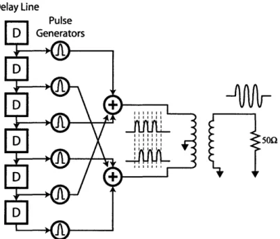
Implementation strategies typically involve generating pulses by combining edges of various delay elements, then amplifying the result using a power amplifier [5, 8]. Architectures that use delay lines to synthesize RF frequencies typically have half-RF cycles available at the output of each delay cell. By exploiting the fact that each half-RF cycle can be manipulated, simple pulse shaping schemes and differential-to-single-ended conversions are possible [6, 7, 33]. A popular architecture involves feeding half-RF cycles to alternating sides of a wideband balun, as shown in Figure 1-7. This architecture ensures there is close to zero DC content at the transmitter output, thus enabling clean Binary Phase-Shift Keying (BPSK) modulation.
Delay Line
_MW
Figure 1-7: A carrier-less architecture employing a balun for zero-DC voltage pulse generation.
All-Digital Transmitters
All-digital pulse generators attempt to reduce the power consumption over their ana-log counterparts by eliminating large static currents required to bias transistors in their linear regions. Instead, digital static CMOS gates are used to generate high frequency rail-to-rail voltage swings. These digital architecture dissipate only CV2f
switching power and subthreshold leakage power.
A similar technique is popular in narrowband radio design, where linear power amplifiers are replaced by switched-mode power amplifiers. A major drawback of this approach is that constant-envelope modulation schemes must often be used, as switched-mode PAs have poor linearity and thus cannot support amplitude modula-tion techniques. Similarly, all-digital UWB transmitters are often restricted to phase and position modulations schemes only.
Pulses in all-digital transmitters can either be synthesized using carrier-less tech-niques, or by modulating the output of a digitally controlled oscillator (DCO). Ex-amples of carrier-less techniques include the transmitters presented in [11, 34]. In these examples, UWB pulses are generated directly in the band of interest by
NOR-ing two delayed edges together, convertNOR-ing from sNOR-ingle-to-differential, and applyNOR-ing the differential signal to a dipole antenna. Similarly, the transmitter considered in [35] generates pulses by combining inverter gate delays using NOR and NAND struc-tures. Relying on uncalibrated gate delays, however, leads to significant deviations in frequency and bandwidth targets over process voltage and temperature (PVT) variation.
The transmitter considered in [10] generates pulses in a carrier-less fashion by combining output edges from a delay line. BPSK modulation is achieved by applying full-swing pulses to either input of a balun, as illustrated in Figure 1-8. However, a bandpass filter is required to reduce the low-frequency content typically associated with digital pulse generation driving a single-ended antenna. This issue is discussed further in Chapter 2. Polarity = +1 \A
_nýL_
Polarity = -1 50OFigure 1-8: An all-digital architecture employing a balun for BPSK modulation.
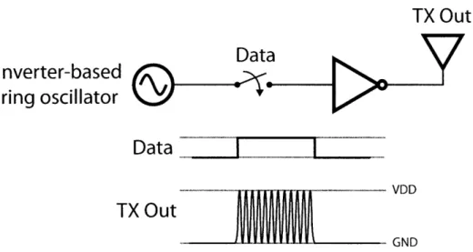
The other technique to generate UWB pulses digitally is to modulate the output of a DCO. For instance, the transmitter considered in [36] generates pulses by directly modulating the output of a three-stage inverter-based ring oscillator. By utilizing the phases of an on-chip frequency divider, discrete two-level pulse shaping is employed.
Since digital circuits are used in this architecture, reconfigurability and calibration are easily implemented.
1.3.2
Non-coherent Pulsed-UWB
It is well known that coherent IR-UWB systems suffer from significant multi-path fading. One method to capture and utilize many propagation paths is to include RAKE-based techniques [27]. This, however, requires high speed and power-hungry clocking, which is not suitable for energy-starved applications. An alternative
ap-proach to capturing multi-path effects is to use a non-coherent, energy-detection architecture [37]. In this technique, the incoming signal is squared, then integrated over a set window of time as discussed in section 1.2.3. If the integration time window is set to be larger than the width of the pulse, the energy of several propagation paths will be collected. Furthermore, the shape of the received pulse is no longer of concern to the receiver.4
Some of the first published non-coherent UWB transceivers incorporating energy detection techniques were presented in [38] and [39]. Pulses were generated by uti-lizing static digital logic similar to the technique found in [11], however, with the advantage of amplitude and phase control via an analog power amplifier. The re-ceiver architecture included a digital baseband and is very similar to that shown in Figure 1-4, with eight integrators operating in parallel to shorten synchronization times. Measured results were shown in [40], and a total pulse generator power con-sumption of 12.9mW was reported.
One of the most common multiple access and modulation schemes for energy-detection-based IR-UWB is time-hopped (TH) Pulse Position Modulation (PPM), where logical values are indicated by the presence of pulses in user-specific windows of time. For deeply duty-cycled transceivers, it is often most convenient and energy-efficient to align PPM intervals closely in time. Unfortunately, this creates large spectral lines at integer multiples of the pulse repetition frequency (PRF), which can adversely affect the ability to meet FCC spectral masks without significant power backoff [41]. Although phase information is meaningless to energy-detection receivers, one method to eliminate such lines is to include random phase scrambling, typically
in the form of BPSK.5 This is discussed in further detail in Chapter 2.
The transmitter considered in [12] proposes a new phase modulation technique termed delay-based BPSK (DB-BPSK). Rather than using an area-expensive balun to invert pulses, a digitally-generated pulse is simply delayed by half of an RF cycle to create a pseudo 180' phase shift. It has been shown that DB-BPSK has the same spectral smoothing effect as pure BPSK in the frequency range of interest [42]. The non-coherent operation relaxes center frequency tolerances, lending this technique to a purely digital implementation employing digital delay lines. The transmitter achieves an excellent energy efficiency of 47pJ/bit; however, an off-chip filter is re-quired for FCC compliance. A corresponding energy-detection receiver considered in [43] utilizes simple analog integration of charge onto capacitors to achieve a low energy consumption of 2.5nJ/bit up to data rates of 16.7Mbps.
As an alternative to energy detection, the non-coherent transceiver considered in [3] eliminated the need for synchronization and correlation by modulating data using On-Off Keying (OOK) and recovering the digital signal through envelope detection. A RAKE-based technique to improve the BER and multi-path fading of such OOK techniques was discussed in [44], though at a cost of increased hardware complexity and power consumption.
The transmitter presented in this thesis utilizes non-coherent pulsed-UWB sig-naling to relax frequency tolerances. This enables an all digital architecture where pulses are synthesized by directly modulating the output of a single-ended DCO. In this manner, the DCO is shared with an integrated downconverting receiver.
5
In fact, the IEEE 802.15.4a proposal mandates that all transmitters must be capable of includ-ing phase information as a means of data modulation; low-power receivers can opt to ignore this information.
1.3.3
Summary
A summary of recently published UWB transmitters is shown in Table 1.1.
Table 1.1: Previously Published UWB Transmitters.
Ref. Process Vdd Symbol Power E/pulse Modulation
[V] Rate [mW] [pJ]
[MHz]
[1] 65nm 1.2 1(x8t ) 0.3 37.5 PPM/BPSK [2] 0.18pm 1.5 200 3.4 16.8 OOK [3] 0.18pm 1.8 50 12.6 252 OOK [4] 0.18pm 1.8 100 31.3 313 BPSK [5] 0.18pm 1.8 400 76 190 PPM [6] 0.18pm 2.2 36 29.7 825 BPSK [7] 0.18pm * 1000 50 50 OOK [8] 0.18pm 1.8 750 9 12 BPSK [9] 90nm 1.0 1(x16t ) 0.65 40 PPM/BPSK [10] 0.13gm 1.2 160 10 62.5 PPM/BPSK [11] 0.18pm 2.5 1 0.7 700 OOK [12] 90nm 1.0 10 0.47 47 PPM/DB-BPSK This Work 90nm 1.0 15.6(x16t ) 4.4 17.5 PPM/BPSK * No VDD was specified.t These transmitters burst multiple pulses back-to-back. The quoted energy per pulse numbers are for a single pulse within a burst.
1.4
Thesis Contributions
This thesis explores pulse-based ultra-wideband transmitters designed for highly en-ergy and area constrained applications. Due to their relaxed center frequency tol-erances, non-coherent UWB systems offer the opportunity to simplify transmitter architectures and increase energy efficiency. This enables the design of an all-digital UWB transmitter. However, all-digital UWB transmitters driving single-ended an-tennas typically produce undesired low-frequency content which violate FCC spectral masks. This low-frequency content is most often attenuated using large passive com-ponents, resulting in a severe area penalty.
The main contribution of this thesis is the design and implementation of an all-digital UWB transmitter which achieves FCC compliant operation without the use of
large passive components. Area and energy efficient FCC compliance is accomplished by using a combination of two techniques:
1. Low frequency content is attenuated up to 12dB by capacitively combining two paths which have in-phase RF components, yet have opposite common-modes which are canceled. This technique is realized in an energy efficient manner by dual capacitively coupled digital power amplifiers.
2. The dual power amplifiers each consist of a number of tri-state inverters. Four-level discrete pulse shaping is employed by dynamically enabling and disabling these inverters during pulse generation, resulting in up to 20dB of RF sidelobe attenuation.
The transmitter is implemented in 90nm CMOS and requires a core area of 0.07mm2 The all-digital architecture consumes 17.5pJ/pulse, which is among the most energy
efficient UWB pulse generators reported in the literature.
This thesis also presents mathematical models used to predict measured spectral results of ultra-wideband pulse bursts. A technique to maximize communication distance of low-rate systems under peak and average power constraints is contributed as a result of this modeling.
Chapter
2
Pulsed-UWB Signaling
The 2002 FCC first order and report placed limits on both the peak and average isotropic radiated power from a UWB device over the 3.1-to-10.6GHz band. Since medium-to-high data rate transmitters are typically average power limited, there has been much effort spent trying to meet average spectral mask requirements while min-imizing both energy consumption and implementation area. This chapter analyzes several different pulse shaping implementation strategies and offers a particular strat-egy that uses both minimal power and chip area. Also explored in this chapter are mathematical models to predict spectral measurements, which leads to a technique used to maximize communication distance for low-rate systems under both peak and average power constraints.
2.1
Generating UWB Pulses Digitally
As Moore's law continues to march down its path of ever-increasing transistor speed and density, it becomes more and more appealing to move previously analog dom-inated functions and circuits over to digital-oriented algorithms and circuits. This move away from analog structures is seen time and time again in examples such as PLLs [45], switched-capacitor circuits [46], and even entire Analog to Digital Converters (ADCs) [47]. The advantages of digital structures are plentiful, including
continued density scaling, zero static bias currents1, and noise immunity.
Assuming, for the moment, that everything that can be done in digital CMOS
should be and will be done in digital CMOS2, it is worthwhile to investigate how UWB pulse generation can be done using entirely singled-ended digital circuits. Section 2.2 and Chapter 4 will discuss some results of this claim in more detail. For now, it does not take much effort to design a very simple all-digital pulse generator. As an example, consider the transmitter shown in Figure 2-1. Data in this transmitter can
be modulated using OOK, or PPM, as illustrated in Figure 2-2.
TX Out
Dat
Inverter-based
ring
oscillator
t
Data
J
VDDTX Out
GNDFigure 2-1: A simple way to generate UWB pulses using all-digital circuits.
This transmitter can be designed using only standard cells in a digital CMOS process. For instance, the oscillator can be implemented as three inverters in a ring, the switch can be implemented as a 2-to-1 multiplexer with one input connected to the output of the ring and the other to ground, and the power amplifier can simply be a large inverter. Since only standard cells are used, it should be possible to synthesize and auto-layout this transmitter architecture using digital Computer Aided Design (CAD) tools.
Of course, this architecture suffers from several drawbacks. Several notable
omis-1
Note that subthreshold leakage currents of large digital designs are fast approaching the levels of static bias currents. However, the recent introduction of low-leakage processes specifically produced for low-power circuits are helping to mitigate this problem.
2...with or without you, as Professor Ali Hajimiri might say. In other words, if you don't do it in digital CMOS, somebody else will, as the cost advantages over other technologies are indisputable.
Logic'O' Logic'l'
TTnt, nt2i Tinti Tnt2
ir 1 l
Figure 2-2: Pulse position modulation represents data by the presence of a pulse in a particular window in time.
sions are the lack of programmability, calibration, and carrier phase lock. Programma-bility can be achieved in the hand-designed oscillator by using binary-weighted capac-itive loads which can programmed through digital logic. In the synthesized circuits, similar programmability can be achieved by inserting several tri-state inverters in parallel, thereby effectively changing each stage of the ring oscillator's drive strength and capacitive load. Similar techniques can by applied to the power amplifier for gain control. Carrier frequency calibration can be achieved using a combination of divider, counter, and phase detector circuits. Carrier phase lock is in fact not necessary if the receiver is non-coherent, since the phase is discarded anyways. Otherwise, a PLL may be used for coherent systems.
Another major problem with this architecture is found in the spectral character-istics of the generated pulses. The output spectrum of a PPM-modulated pulse train is given by equation 2.1 [41, 42].
1 n00
T
ppPM(f) = 4T . S(
+ie -+ i2(if) re T n=--oo T s +IS(f)1
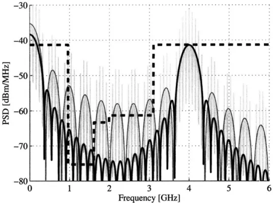
2 - IS(f)(1 + e-j2fTppm) 2 (2.1)Here, S(f) is the Fourier transform of the reference pulse, TppM is the PPM delay, and T, is the symbol repetition period. The resulting power spectral density of a square pulse train with non-zero DC content centered at 4GHz (as in Figure 2-2)
is superimposed over the FCC indoor mask in Figure 2-3.
CI.
0 1 2 3 4 5 6
Frequency [GHz]
Figure 2-3: Power spectral density of a train of PPM-modulated square UWB pulses. The resulting spectrum has an underlying shape of a sinc(x) (or sin(x)/x) enve-lope centered at the carrier frequency. This makes sense, since the Fourier transform of a rectangular pulse in the time domain leads to a sinc(x) function in the frequency domain. However, due to several reasons this spectrum is not FCC compliant. Sec-tion 2.2 will attempt to fix the compliance issue while adding as little circuit area and energy overhead as possible.
2.2
Achieving Spectral Compliance
The time and frequency domain views of a PPM-modulated square UWB pulse train are shown in Figures 2-2 and 2-3, respectively. There are three main problems with this resulting spectrum, all three of which must be addressed in order to meet the FCC spectral mask:
1. Large spectral lines spaced at integer multiples of the pulse repetition frequency. .. . . . . . . .
2. Sidelobes centered at the carrier frequency.
3. Sidelobes centered at DC.
2.2.1
Spectral Lines
The problem of spectral lines is conceptually easy to fix. If the UWB pulses were phase modulated with random (or pseudo-random) data during transmissions, the tones would be scrambled out. This effect is most easily achieved by implementing a BPSK scrambler or modulator. The resulting power spectral density is given by equation 2.2, and is illustrated in Figure 2-4.
(2.2)
PBPSK(f) =
IS(f)1
2 1! .. 3( Ill I'fi
• :•. i •~ ~ .il.i •..•:.•. ; ... .iI Frequency [GHz]Figure 2-4: Power spectral density of a train of PPM-modulated, BPSK-scrambled, square UWB pulses overlaid on top of the non-BPSK-scrambled case.
2.2.2
RF Sidelobes
This spectrum of Figure 2-4 still suffers from drawbacks two and three: namely, it contains undesired sidelobes centered at both RF and DC. Although these sidelobes can easily be eliminated by bandpass or highpass filters, the area penalty of this approach is significant. For instance, this particular example would require at least a fourth order passive filter to ensure the necessary roll-off of roughly 20dB in 0.29 decades (from the 1.61GHz to 3.1GHz mask boundaries). A fourth order passive filter requires several inductors and capacitors, which are not only lossy in modern semiconductor technologies, but also consume significant area.3 One can also engineer an antenna to have the desired bandpass properties, however since the UWB band is so large (3.1-to-10.6GHz), it may be difficult to achieve the required selectivity. Also, for system robustness it is generally desirable to design circuits to be compatible with a variety of different peripheral devices, such as antennas in this case.
An alternative to filtering is to employ pulse shaping to reduce the sidelobes centered at RF. As demonstrated in [6, 7, 48, 49, 50], and many other designs, pulse shaping is a very good method for obtaining high-order roll-off without the use of large passive filters. An excellent overview of several popular pulse shapes can be found in [51].
To illustrate the virtues of pulse shaping, consider shaping a pulse with a raised-cosine envelope, as illustrated in Figure 2-5. The resulting spectrum achieves up to
17dB of sidelobe rejection, as shown in Figure 2-6.
Shaped Pulse
--AMMM
----Raise
Figure 2-5: Time domain view illustrating how to generate a raised-cosine pulse.
3The option of an off-chip filter is far worse in terms of an area trade-off, although they do tend
EI
-oV0 1 2 3 4 5 6
Frequency [GHz]
Figure 2-6: Power spectral density of a train of PPM-modulated, BPSK-scrambled, raised-cosine UWB pulses overlaid on top of the spectrum in Figure 2-4.
2.2.3
Low Frequency Sidelobes
The raised cosine envelope greatly suppresses the sidelobes centered around the carrier frequency. However, the sidelobes centered at DC remain. This problem does not depend on pulse shape, but is rather fundamentally related to the method in which the digital pulses are synthesized. The issue stems from the fact that single ended digital circuits have only two stable operating points: the lowest and highest potentials in the circuits (typically GND and VDD). To eliminate the DC content and its associated sidelobes, the generated pulses must have three effective levels: GND, +V, and -V, as illustrated in Figure 2-7.
For continuous wave systems, this is a relatively easy problem: simply insert an AC-coupling capacitor4 before the antenna, as illustrated in Figure 2-8. This solution is not ideal for pulses of short duration, the reason for which will become clear momentarily. Digitally generated pulses with two reference voltage levels (e.g.
40therwise known as an DC-blocking capacitor. I
Single ended digital CMOS
Ideal (differential analog)
.I
_IrMI
V
Figure 2-7: Digital CMOS circuits can only generate one of two different reference levels. On the other hand, differential analog circuits can generate multiple reference levels at different bias voltages.
GND and VDD), can be decomposed into an RF carrier and a baseband pulse, as illustrated in Figure 2-5. The baseband pulse will require a finite amount of time to charge and discharge the voltage across the capacitor, as shown in Figure 2-9. The
time required to charge and discharge, given by tcharge and tdischarge respectively, is
proportional to the 1/RC time constant of the circuit.
TX Out
From pulse generator
Figure 2-8: A coupling capacitor providing a DC block to a wideband antenna. A large resistor may be connected from the output to ground in order to provide a stable DC voltage to the antenna if necessary.
The effect of finite low frequency capacitor charging and discharging times when AC-coupling UWB pulses is illustrated through a time-domain simulation of a square pulse in Figure 2-10. It can be noted here that the AC-coupled pulse has a non-zero DC value, as well as some low-frequency turn-on and turn-off transients. The power spectral density of a train of BPSK-scrambled raised-cosine UWB pulses before and after the AC-coupling filter is shown in Figure 2-11. The AC-coupled spectrum
uirv
Vcap VIruit /out GND- - -500 tcharge tdischarge VDD - - - - - - - - -Vcap GND - ----
--Figure 2-9: A baseband pulse requires a finite amount of time to charge and discharge a coupling capacitor.
1 2 3 4 Time [ns]
(a) Digitally generated pulse
V
5 6 0 1 2 3 4
Time [ns]
(b) After AC-coupling filter
Figure 2-10: The effect of passing a UWB pulse through an AC-coupling capacitor.
does not comply with the FCC mask, since the first order roll off is not sufficient to eliminate all of the low frequency sidelobes.
There are several techniques to reduce or even eliminate the low frequency-content of digitally generated UWB pulses. The most common technique relies on generat-ing individual half-RF cycles and applygenerat-ing them differentially to a wideband balun, as discussed in section 1.3.1 [6]. This technique produces excellent spectral results,
however it does not fit in with the spirit of designing scalable architectures with min-imal area, since inductors are relatively large and do not scale very well in advanced
VDD-- - -
-GND-
Frequency [GHz] Figure 2-11: Power
coupling filter.
spectral densities of raised cosine pulses before and after an
AC-CMOS technologies.5 Another potential drawback of this type of architecture is that the half-RF cycles are generated from a delay line instead of a free-running ring oscil-lator. This can be seen as a benefit if the designed system is only a transmitter which generates a single pulse, then immediately turns off for a period of time. If, instead the designed system is a transceiver that transmits multiple pulses back-to-back, it is beneficial to design a single oscillator whidh is shared between the receiver and transmitter, as shown in Figure 2-12.
The proposed solution to attenuating the low frequency content using scalable digital structures involves capacitively coupling two paths which have differential baseband signals, yet contain in-phase RF tones. To elaborate, consider the network shown in Figure 2-13(a), where the two capaci ors nominally have opposite DC volt-ages across them (GND and VDD, generated from digital logic). If they are driven
5
That is, they do not scale as well as capacitors in terms of area density. This is because inductors are typically implemented in the topmost m tal layers (which have not been scaling very quickly), whereas capacitors are scaling somewhat more rapidly with advancements in dielectrics and/or increases in lower-metal layer densities (for me al-oxide-metal capacitors).
-30 -40 -50 Q -60 04 -70 -80( - -i i I i I~~ I ~aI Il-I I. 6 . . . . . . I . . . .
Figure 2-12: A simple transceiver system sharing a single oscillator.
with a differential baseband pulse, the upper capacitor will ideally charge at the same rate that the lower capacitor is discharging, thereby inducing zero voltage at the output. VUU -(~Nfl... VUU -vuuln
-1
-1
- - GND 50Q (a) VLL - G'ND-VULD (ND ljlh
AAAA
(b)
Figure 2-13: Differential baseband pulses cancel as shown in (a), while in-phase RF signals propagate relatively undisturbed to the output, as shown in (b).
If the low frequency baseband pulses are multiplied with in-phase RF tones as illustrated in Figure 2-13(b), then the low frequency common-modes will cancel, and the in-phase RF components will propagate to the output.
GND
-,..I
S-
GND
Since the two inputs into the capacitive com bination network start off with oppo-site common modes, there is an inherent half IF cycle delay between the start of the effective baseband pulses shown in Figure 2-13(b). This, combined with circuits mis-matches, will create non-idealities including t'urn-on and turn-off transients leading to spectral impurities. Ideally, the output spectrum will contain zero low frequency content, as illustrated by the spectrum of ideal raised cosine pulses in Figure 2-14. In practice, the output spectrum will have an appreciable amount of low-frequency content. This is discussed using mismatch analysis of the designed circuits in Chap-ter 3. The measurement results in ChapChap-ter 4 will indicate that there is sufficient low frequency attenuation to meet the FCC spectral mask.
Nc
0 1 2 3 4 5 6
Frequency [GHz]
Figure 2-14: Power spectral densities of ideal raised-cosine pulses and AC-coupled digitally generated raised cosine pulses.
2.3
Predicting Measurement Results
The goal of this section is to provide a mathematical framework for predicting the measurement results of pulsed-UWB signals using a spectrum analyzer (SA). Before getting into the details it is worthwhile to review the FCC regulations and introduce the concept of pulse bursting, all while introducing some notation.
2.3.1
FCC Regulations
Recall that the FCC places limits on both the peak and average radiated output power in the 3.1-to-10.6GHz UWB band. For the sake of completeness, the two key FCC regulations are as follows [16]:
1. The average PSD must be less than or equal to -41.3dBm in the 3.1-to-10.6GHz band. This corresponds to a theoretical maximum total power of -14.3dBm for a 500MHz bandwidth signal. In practice this number is reduced by 2-to-4dB via pulse generation constraints. Table 2.1 shows the maximum PSDs in other frequency ranges.
2. The peak power may not exceed OdBm at the UWB signal's center frequency in a 50MHz resolution bandwidth (RBW). Since most spectrum analyzers are not equipped with a 50MHz intermediate frequency (IF) filter, the peak power mea-surement is typically performed at a lower RBW and the limit is conservatively set to be Ppk • 201oglo(RBW/50MHz).
It should be noted that although measurements to confirm FCC compliance are typically done with a spectrum analyzer, alternative techniques exist [52].
2.3.2
Pulse Bursting
For long range and/or reliable communication, it is often necessary to transmit mul-tiple pulses per bit of information. The extra pulse information allows the receiver to perform averaging, thereby increasing the effective signal to noise ratio and thus
Table 2.1: FCC Mask Limits
Frequency Range Indoor Limit Outdoor Limit
[MHz] [dBm/MHz] [dBm/MHz] Below 960 FCC 15.209 960-1610 -75.3 -75.3 1610-1990 -53.3 -63.3 1990-31000 -51.3 -61.3 31000-10600 -41.3 -41.3 Above 10600 -51.3 -61.3
decreasing the bit error rate. The number of pulses per bit is typically called the
spreading factor.
In the interest of duty cycling, it is generally advantageous to process information using many bits at a time, then subsequently shutting circuitry off. This minimizes the energy overhead of having to turn on and off the circuits performing the information processing. For example, if a system operates at an effective data rate of 100kbps and requires a spreading factor of 10 for reliable communication, the PRF would have to be 1Mpulse/s. Instead of representing a symbol with a single pulse, it is alternatively possible to burst several pulses together and transmit them at once. For instance, if a burst of ten pulses constituted a symbol, then a symbol repetition frequency (SRF) of 100kSymbols/s would still have an effective PRF of 1Mpulse/s, yet there is a 10x reduction in the turn-on/turn-off energy overhead, as illustrated in Figure 2-15. Pulse bursting is especially beneficial to non-coherent system implementations, as the
No Bursting
- -Bursting
Startup/Shutdown t No Bursting
Energy overhead Bursting
Figure 2-15: Turn-on/turn-off energy overhead reduction when applying pulse burst-ing.
integration period often determines the maximum symbol rate, which is typically the same as the baseband clocking frequency. Thus a low symbol rate leads to a low clock rate, which simplifies digital implementations and improves energy efficiency.
Figure 2-16 illustrates the concept of pulse bursting by showing two groups of five individually BPSK modulated pulses. Some notation is also introduced here. For instance, in communication theory the individual pulse width is typically called the chip period, indicated by -r. N, is the number of chips per burst, and Vpk is the peak voltage of the waveform. It should be noted that the IEEE 802.15.4a standardization committee incorporates pulse bursting into the UWB PHY layer [29].
--
NcTc
--
Symbol Rep. Period
=
1/SRF
Figure 2-16: Two bursts of five individually BPSK modulated pulses (i.e. N, = 5).
2.3.3
Mathematical Modeling
Most UWB pulses have a narrow pulse width T, < 0.1/RBW relative to the interme-diate frequency of an SA. Thus, the SA measures the impulse response of its own IF filter, rather than the response of the UWB pulse. To predict certain measured re-sults from an SA, a pulse desensitization correction factor (PDCF) will be introduced
[4, 53].
Ideally, the spectral response of a periodic BPSK-modulated pulse (or burst) train should contain spectral lines at integer multiples of the SRF.6 This effect will be
ob-served on an SA if its RBW if less than the SRF, since the SA will have sufficient resolution to display the spectral lines. This measurement regime is called the
high-SRF region, and occurs when RBW/high-SRF < 0.3. If, on the other hand, the RBW 6
These lines are different than the undesired spectral lines produced by non-phase-scrambled, PPM-modulated pulse trains.
I I I
is greater than the SRF, the SA does not have sufficient resolution and individual spectral lines are blended together. This measurement regime is called the low-SRF
region, and occurs when RBW/SRF > 1.7. The peak and average powers in these
two regions can be predicted using the equations derived below. Unfortunately, mea-surements in the region around SRF RBW depend heavily on modulation statistics
and is much more difficult to predict [54].
For both low and high symbol-repetition frequency BPSK-modulated signals, the the average power can be found by using Equation 2.3.
Pay9 - 10 log
Pk)
+ 20 log(eff) + 10 log(PRFe~ i - RBW) (2.3)Here, Vpk is the peak voltage of the pulse, Zo is the characteristic impedance, and PRFejf is the effective pulse repetition frequency (i.e. for bursting, PRFff = SRF x N,).
Teff is the effective individual pulse width, as illustrated by Figure 2-17 and given by
Equation 2.4.
eff P ) dt (2.4)
Teff Vp k
Here, p(t) is a single pulse, and T, is the time interval which contains all the energy
of p(t).
p(t)
er
s
Tc
Figure 2-17: Effective pulse width of a non-rectangular pulse envelope.
The peak power in the high-SRF region is given by Equation 2.5