S1
Supporting Information
Robust Bipolar Light Emission and Charge Transport in Symmetric Molecular Junctions
Ushula M. Tefashe, Quyen Van Nguyen, Frederic Lafolet, Jean-Christophe Lacroix, * and Richard L. McCreery*
Ushula M. Tefashe, Richard. L. McCreery
University of Alberta, 11421 Saskatchewan Dr. Edmonton, AB T6G 2M9, Canada E-mail: [email protected]
Van Quyen Nguyen, Frederic Lafolet, Jean-Christophe Lacroix
Université Paris Diderot, Sorbonne Paris Cité, ITODYS, UMR 7086 CNRS, 15 rue Jean-Antoine de Baïf, 75205 Paris Cedex 13, France. Email : [email protected]
Richard L. McCreery
National Institute for Nanotechnology, 11421 Saskatchewan Dr. Edmonton, AB T6G 2M9, Canada
* corresponding author
1. Structure of Ru(bpy)3P precursor and in situ conversion to its diazonium form 2. Ru(bpy)3P film deposition parameters
3. Determination of molecular layer thickness by AFM 4. XPS of Ru(bpy)3P films deposited on Au
5. Raman spectra of Ru(bpy)3P materials
6. Additional spectra of light emission from Ru(bpy)3P MJs
7. Comparative light emission spectra for Ru(bpy)3P and NAB junctions 8. Scan rate dependence of JV curves in air and vacuum
9. Expanded view of light emission and current pulses of Ru(bpy)3P devices 10. Parylene Coating Procedure
S2
1. Structure of Ru(bpy)
3P precursor and in situ conversion to its diazonium
form
Figure S1. Structure of the amine precursor of Ru(bpy)3P, and structure of Ru(bpy)3P diazonium ion produced by in situ diazotation of the amine precursor by tert-butyl nitrite in acetonitrile under Ar atmosphere at room temperature.
2. Ru(bpy)
3P film deposition parameters
Preceding electrochemical deposition, 25 equivalent of t-butyl nitrite were added to 20 mL of 0.5 mM amine precursor in 0.1 M tetrabutylammonium hexafluorophosphate (TBAPF6). After waiting 5 minutes, the parameters of Table S1 were used for Ru(bpy)3P film formation on a Au/eC substrate.
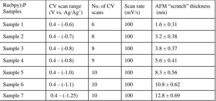
Table S1. Ru(bpy)3P grafting parameters on Cr4/Au30/eC10 : voltammograms scan range, number of CV scans, sweep rate, AFM “scratch” thickness.
Ru(bpy)3P Samples CV scan range (V vs. Ag/Ag+) No. of CV scans Scan rate (mV/s)
AFM “scratch” thickness (nm) Sample 1 0.4 – (-0.6) 6 100 1.6 ± 0.31 Sample 2 0.4 – (-0.7) 8 100 3.2 ± 0.38 Sample 3 0.4 – (-0.8) 8 100 3.8 ± 0.37 Sample 4 0.4 – (-0.8) 9 100 5.6 ± 0.41 Sample 5 0.4 – (-1.0) 10 100 8.3 ± 0.56 Sample 6 0.4 – (-1.1) 10 100 10.8 ± 0.62 Sample 7 0.4 – (-1.25) 10 100 12.8 ± 0.69
S3
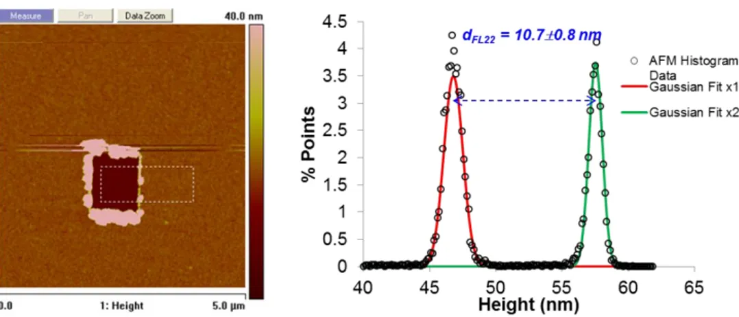
3. Determination of molecular layer thickness by AFM
Figure S2. Example of AFM trench image from “scratching” and depth histogram with the Gaussian fitting profile. The error in thickness (± 0.8 nm in the case shown) is the quadrature combination of the standard deviations of each Gaussian fit.
4. XPS of Ru(bpy)
3P films deposited on Au
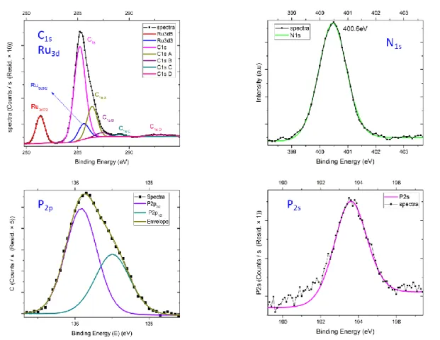
The Ru(bpy)3P deposition procedure of section 2 above was carried out on a blanket Au sample to avoid the contribution of e-Carbon to the XPS spectrum. After electrochemical grafting, the modified electrode was rinsed carefully in ACN and MilliQ water several times, then sonicated in MilliQ water for 10 min. High resolution spectra of the C1s /Ru3d, N1s, F1s, P2p, and P2s spectral regions are shown in Figure S3, and atomic percentages are listed in Table S2. The lack of an N1s peak at 405 eV for nitrogen from diazonium group indicates covalent grafting of Ru complex, not physisorption of the Ru complex diazonium ion1. The N
1s core level presented a well-defined peak centered at 400.5 eV which is attributed to the nitrogen of bipyridine rings1,2. The P/F/Ru ratios as shown in table S2 indicate the presence of two PF6 groups for each Ru+2 center and the Ru(bpy)
3 molecule is stable during electrochemical deposition.
S4 Figure S3. High resolution XPS spectra of Ru(bpy)3P films deposited on blanket Au surface. Black curves with points are experimental, smooth colored curves are fits to known XPS features. The experimental and predicted Ru3d5/2 peaks are indistinguishable.
Table S2. XPS Atom% results for Ru(bpy)3P films (d = 8 nm) deposited on Au
(BE= binding energy, FWHM= full width at half-maximum, CPS= counts/sec, SF=sensitivity factor)
S5
5. Raman spectra of Ru(bpy)
3P materials
Raman spectra of the Ru(bpy)3P precursor and the thin film formed by diazonium reduction are shown in Figure S4. The Raman features are preserved during film formation, indicating that the Ru(bpy)3 centers remain intact in the film. The additional Raman bands in the 1500- 1580 cm-1 region in the film spectrum are consistent with the ring stretches of the phenyl ring between Ru(bpy)3 centers in the film, and are not observed in either unmodified Ru(bpy)3 or the Ru(bpy)3P(PF6)2 monomeric precursor.
Figure S4. Raman spectra of the Ru(bpy)3P monomer and a thin film on Cr/Au/eC surface. Laser wavelength = 514.5 nm
6. Additional spectra of light emission from Ru(bpy)
3P MJs
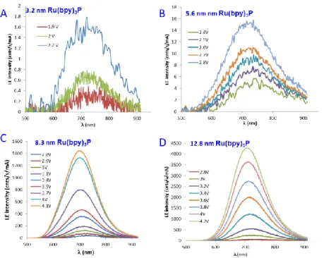
Figure S5. Additional uncorrected spectra of light emission for 3.2 nm, 5.6, 8.3 and 12.8nm Ru(bpy)3P junctions. Applied DC bias for each thickness is indicated as inset. All curves are measured in positive polarity. Each spectrum was normalized to the junction current.
S6
7. Comparative light emission spectra for Ru(bpy)
3P and NAB junctions
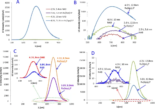
Figure S6. Plots of emission spectra for Ru(bpy)3P and NAB junctions of the same device structure with similar molecular layer thickness and at similar bias. (A) Comparison LE spectra for thin and thick junctions of Ru(bpy)3P and NAB devices at high and low applied bias. (B) Logarithmic scale of the plot in panel (A). Emission spectra of (C) 8.3 nm Ru(bpy)3P and 8 nm NAB; (D) 10 nm Ru(bpy)3P and 12.8 nm NAB compared at two applied bias. The insets of panels (C) and (D) represent a magnified view of NAB light emission spectra. The values of the applied bias are as indicated for spectrum.
S7
8. Scan rate dependence of JV curves in air and vacuum
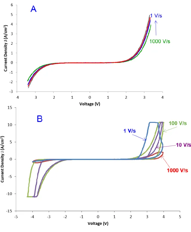
Figure S7. J-V of Cr4/Au30/eC10/ Ru(bpy)3P/eC10/Au20 junctions: (A) under vacuum, (B) in air at various scan rates (d = 12.8 nm). The hysteresis observed in air increased at slower scan rate.
S8
9. Expanded view of light emission and current pulses of Ru(bpy)
3P devices
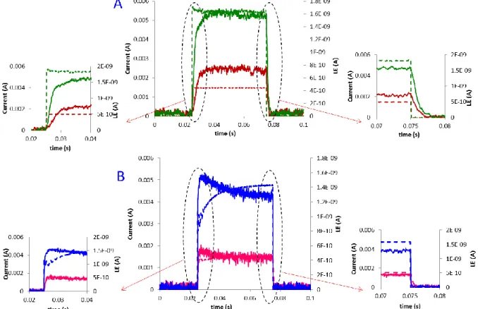
Figure S8. Light emission intensity as a function of time and applied bias in (A) vacuum and (B) air, with the expanded view of bias “on” and “off” time scale in current and light emission pulses are shown to the left and right of (A) and (B).
10. Parylene Coating Procedure
The Cr4/Au30/eC10/ Ru(bpy)3P/eC10/Au20 MJ samples were coated in with parylene C polymer in a SCS Labcoter 2 (Specialty coating systems PDS 2010) vacuum deposition system. The clear polymer coating provides an extremely effective chemical and moisture barrier with high dielectric and mechanical strength.
With minimal exposure to air, completed molecular junctions were transferred from the electron-beam deposition system to a separate vacuum system, and 1g of Parylene C (Specialty Coating Systems) was added to the aluminum foil dimer boat inside the vaporizer. The 1g of parylene C deposits an approximately 500 nm thick film at a rate of ~5 µm/hr.
Once the system is loaded and pumped down to a base pressure of 35 mTorr, the parylene C dimer source material in the vaporizer is heated to 175°C which is then pyrolyzed in the furnace at 690°C transforming it into gaseous monomers which deposit conformally all over the room-temperature samples. Once the deposition was complete and the system was cooled down, the samples were removed.
S9
11. CVs and UV-Vis spectra of Ru(bpy)
3P molecules in solution and eC
substrates
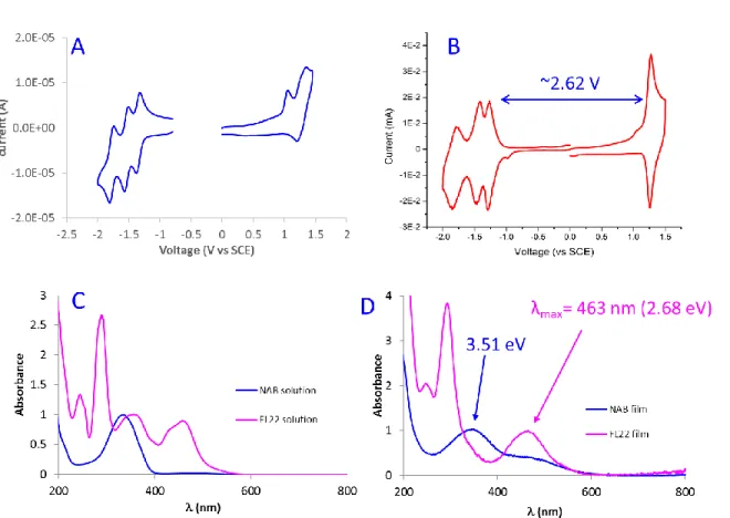
Figure S9. Cyclic voltammogram of (A) amine precursor of Ru(bpy)3P in 0.1 M TBAPF6 in acetonitrile and (B) Ru(bpy)3P functionalized on carbon substrate. Scan rate 100 mV/s. (C) UV-Vis spectrum of NAB and the amine precursor of Ru(bpy)3P in acetonitrile (D) Transmission UV-Vis spectrum of Ru(bpy)3P functionalized on quartz/Cr3/Au15/eC10 substrate after
S10 References:
(1) Agnes, C.; Arnault, J.-C.; Omnes, F.; Jousselme, B.; Billon, M.; Bidan, G.; Mailley, P. Phys. Chem.
Chem. Phys. 2009, 11, 11647.
(2) Nguyen, V. Q.; Sun, X.; Lafolet, F.; Audibert, J.-F.; Miomandre, F.; Lemercier, G.; Loiseau, F.; Lacroix, J.-C. J. Am. Chem. Soc. 2016, 138, 9381.