by the Finite-Difference Time-Domain Technique
byBae-Ian Wu
B.Eng. Electronic EngineeringThe Chinese University of Hong Kong, 1997
Submitted to the Department of Electrical Engineering and Computer Science in partial fulfillment of the requirements for the degree of
Master of Science
at the MASSACHUSETTS IN
OF TECHNOLOI
MASSACHUSETTS INSTITUTE OF TECHNOLOGY May 1999
@
Massachusetts Institute ofYTechnoiogy 1999. All rights reservA uthor ... . .. ... Department of Electrical Engineering and Computer Science
May 24, 1999 C ertified by ... ... . ... Professopdf Certified by... V I Accepted by...- .... ... . ....
Chairman, Department Committee
.. ... ... Dr. Jin Au Kong Electrical Engineering Thesis Supervisor ... ... ... Dr. Y. Eric Yang Research Scientist Thesis Supervisor ... Arthur C. Smith on Graduate Students
Analysis of Photonic Crystal Filters
by the Finite-Difference Time-Domain Technique
by
Bae-Ian Wu
Submitted to the Department of Electrical Engineering and Computer Science on May 24, 1999, in partial fulfillment of the
requirements for the degree of Master of Science
Abstract
A special finite-difference time-domain (FD-TD) formulation which allows electro-magnetic (EM) wave wideband simulations of oblique incidence for periodic media is used for the design and analysis of an infrared photonic crystal filter with dual stop-bands at 3 - 5 pm and 8 - 12 pm. The transmission coefficient in the main stopband
(8 - 12 [tim) is below -10 dB. Scattering coefficients are calculated for different inci-dence angles, and the stopbands are shown to exist for different angles of inciinci-dence.
A hybrid method is developed for analyzing multilayer structures. Scattering coefficients from a single layer filter can be computed by using FD-TD. Applying microwave network theory, the scattering characteristics of a single layer can be rep-resented by a generalized scattering matrix which can be transformed into a transfer matrix. Scattering by multilayer structures is then calculated by the multiplication of transfer matrices. This technique allows efficient analysis of different configurations of layers without resorting to full EM simulation, which requires a lot of computing time and memory. Using the hybrid method, the transmission coefficients of cas-caded metal screens with different angles of incidence are presented and compared with FD-TD results. The contributions of higher-order modes to the transmission characteristics are identified.
Thesis Supervisor: Dr. Jin Au Kong Title: Professor of Electrical Engineering
Thesis Supervisor: Dr. Y. Eric Yang Title: Research Scientist
First of all, I would like to thank Professor Kong for his teaching and kindness, and Dr. Eric Yang for guiding me through this research. They have given me valuable insights. I would also like to thank Simon, Alex and Bob Atkins from Lincoln Laboratory for their valuable help and discussions and introducing me to this project. I would like to acknowledge the help Andrew Kao gave me to understand his code. Without
him, this project would have been very hard. Yan, Henning and Joe helped me so much throughout the project in many aspects, thank you very much. I also want to thank Dr. Ding, Dr. Jerry Akerson, Dr. Sean Shih, Chi, Chris and Peter, for their friendship. Last but not least, I want to thank my parents, my brother and Mimi for their love, patience and support.
1 Introduction 11
1.1 M otivation . . . . 12
1.2 Past Works and Research Description . . . . 13
1.2.1 Design of a Photonic Crystal Bandstop Filter in the Band 3 - 4pm and 8 -12pm . . . . 14
1.2.2 Analysis of Multilayer Structures by Hybrid Method Based on FD-TD and Transfer Matrix Formulation . . . . 14
1.3 Outline of the Thesis . . . . 15
2 Finite-Difference Time-Domain Method 16 2.1 Regular FD-TD Method . . . . 16
2.1.1 Central Differencing and Propagation Equations . . . . 16
2.1.2 Numerical Dispersion and Stability . . . . 19
2.1.3 Computational Domain . . . . 20
2.1.4 Modeling of Dielectrics and Conductors . . . . 21
2.1.5 Absorbing Boundary Condition . . . . 21
2.1.6 Periodic Boundary Condition . . . . 23
2.2 Oblique Incidence FD-TD . . . . 24
2.2.1 P -
Q
Propagation Equations . . . . 242.2.2 Stability Criteria and Boundary Conditions . . . . 28
CONTENTS
3 Simulation Results and Analysis
3.1 Comparison between FD-TD and Experiment in IR Band .... 3.2 Parametric Study at Normal Incidence . . . . 3.3 Effects of Metal Thickness and Dielectric Constant of Substrate
3.3.1 Metal with Finite Thickness . . . . 3.3.2 Dielectric with High Permittivity . . . . 3.4 Optimal Design of Filter and Performance at Oblique Incidence
3.4.1 Aligned Structure . . . . 3.4.2 Face-Center-Cubic Structures . . . . 30 . . . 30 . . . 33 . . . 40 . . . 40 . . . 40 . . . 41 . . . 44 . . . 49
4 Hybrid Method for Multilayer Analysis
4.1 Generalized Scattering Matrix . . . . 4.2 Transfer Matrix for Dielectric . . . .
5 Simulation Results Based on Hybrid Method
5.1 D ichroic Plate . . . . 5.2 Square Patches . . . . 6 Conclusion 54 55 62 64 64 66 74 6
1-1 Usage of photonic crystal filter as a sensor window. . . . . 12
2-1 Yee's lattice for Regular Finite-Difference Time-Domain formulation. 18 2-2 Cross section of the computational domain of FD-TD for periodic sur-faces with absorbing boundary on top and bottom and periodic bound-ary at the sides. . . . . 20
2-3 Periodic boundary condition. The field quantity outside the computa-tional cell can be updated via translacomputa-tional symmetry. . . . . 22
2-4 Comparison of wave front position between normal incidence and oblique incidence. Non-causal periodic boundary relation hinders the use of regular FD-TD for oblique incidence on periodic surfaces. . . . . 24
2-5 Orientation of k-vector at oblique incidence. . . . . 25
2-6 M odified Yee's lattice . . . . 27
2-7 Ratio between A and cAt vs. 0 and
#
. . . . 283-1 Geometry of the 3-D IR MDPC filter. Metallic parallelepipeds with square cross section is arranged in a face-center-cubic (100)-oriented crystal structure. . . . . 31
3-2 Comparison between FD-TD and experimental results of a 3D MDPC IR bandstop filter. . . . . 32
LIST OF FIGURES
3-3 Geometry of the design of one layer used in the parametric study and final design. Circular metal discs are arranged in a triangular grid, and
are embedded in a dielectric substrate of e, = 2.1, 2.3. . . . . 33
3-4 Transmission coefficients of bandstop filter with one layer of metal screen. S = 2 pm, d = 1.58 pm. . . . . 34
3-5 Series A. Transmission coefficients of bandstop filters with three aligned layers of metallic screens. S = 2pm, h = 0.72pm. . . . . 36
3-6 Series B. Transmission coefficients of bandstop filters with three aligned layers of metallic screens. S = 2 pm, h = 0.96 pm. . . . . 36
3-7 Series C. Transmission coefficients of bandstop filters with three aligned layers of metallic screens. S = 2 pm, h = 1.14 pm. . . . . 37
3-8 Series D. Transmission coefficients of bandstop filters with three aligned layers of metallic screens. S = 2pm, h = 1.44pm. . . . . 37
3-9 Infinitely thin metal vs. metal with finite thickness. . . . . 41
3-10 Internal angles for superstrates with different permittivities. . . . . . 42
3-11 Transmission characteristics with substrate having c, = 2.3 . . . . 43
3-12 Transmission characteristics with substrate having E, = 4.8 . . . . 43
3-13 Azimuthal angle of incidence
#
with respect to the filter. . . . . 443-14 Transmission coefficient for TE incidence, 0 = 0 - 60',
#
= 00... 463-15 Transmission coefficient for TM incidence, 0 = 0' - 600,
#
= 00. . . 463-16 Transmission coefficient for TE incidence, 0 = 0' - 60, = 900. . . 47
3-17 Transmission coefficient for TM incidence, 6 = 0* - 600,
#
= 900 . . 473-18 Relative position of the metal patches at different layers for a face-center-cubic structure. . . . . 49
3-19 Unit cell for face-center-cubic structure . . . . 49
3-20 Transmission coefficient (fcc) for TE incidence, 0 = 00 - 60',
#
= 00. . 513-21 Transmission coefficient (fcc) for TM incidence, 0 = 00 - 600,
#
00. 51 3-22 Transmission coefficient (fcc) for TE incidence, 0 = 0' - 600 = 90'. 52 3-23 Transmission coefficient (fcc) for TM incidence, 0 = 0' - 60',#
= 90'. 524-1 General structure of a multilayer filter. . . . . 56
4-2 Orientation of incident wavevector k. . . . . 57
4-3 Scattering of different modes from a periodic surface. . . . . 58
4-4 Truncated sum of modes. Modes are computed if they fall within a circle of finite radius. . . . . 59
4-5 Graphical representation of the scattering matrix. . . . . 60
5-1 Geometry of the periodic surface used in the dichroic filter. . . . . 65
5-2 Cross section of the dichroic plate sandwich filter. . . . . 65
5-3 Orientation of the incident wave . . . . 66
5-4 Comparison between two different hybrid methods for TE incidence. 67 5-5 Comparison between two different hybrid methods for TM incidence. 68 5-6 Geometry of the cascaded metal screen used in the hybrid method. 70 5-7 Magnitude of vertical propagation factor for different modes. . . . . . 72
5-8 Transmission coefficients of different modes (co-polarized). . . . . 72
5-9 Transmission coefficients of different modes (cross-polarized). . . . . . 73
List of Tables
3.1 Resonance frequency based on calculation. . . . . 38 3.2 Relative bandwidth and minimum transmission coefficients of the
band-stop filters (parametric study) . . . . 39 3.3 Relative bandwidths of the dual stop bands at different incident angles
(aligned structure). . . . . 48 3.4 Relative bandwidths of the dual stop bands at different incidence angles
(fcc structure). . . . . 53 5.1 Degeneracy of modes for normal incidence . . . . 69
Introduction
Photonic crystals [1, 2] are a class of photonic devices that utilize periodic structures to create photonic band gaps [3, 1], analogous to the III-V compound semiconductors in which photons with specific energies cannot be transmitted through the structures. The periodicity of photonic crystals can be formed by differences in dielectric constant, or by a combination of metal and dielectric, and hence the term metallodielectric photonic crystals (MDPC) [4].
Analysis of photonic crystal filters is similar to yet different from the analysis of frequency selective surfaces (FSS). It is because the close coupling between the peri-odic elements make it more difficult to predict the scattering characteristics. To design an IR filter using photonic crystals, experimental and theoretical techniques can be used. However, the cost and time for fabrication and testing become prohibitively high. An accurate electromagnetic model is in demand.
Applications of photonic crystal filters have been found in several areas. For thermal sensors, they can be used to isolate the interference from the atmospheric background. With dichroic plates [5], incident electromagnetic waves with different frequencies can be separated at large angle of incidence. In thermophotovoltaic (TPV)
CHAPTER 1. INTRODUCTION 12
3 - 5pm and 8 -12pum
All frequencies 3
Figure 1-1: Usage of photonic crystal filter as a sensor window.
cells, it improves the efficiency of the cell by providing spectral control of the emission from the thermal source. There are numerous applications where dichroic filters that operate over a wide solid angle are desirable. Consider, for example, a satellite-based IR imager which maps the Earth's surface in the 3 - 4 pm and 8 - 12 pm bands where the atmosphere is transparent. To minimize out-of-band loading of the IR sensor from the albedo, a useful primary mirror coating would reflect strongly from
3 - 4 pm and 8 - 12 pLm and would transmit out-of-band radiation away from the sensor. Another potential application is for low-emissivity window treatments for energy-efficient buildings.
1.1
Motivation
Previous experimental results [4, 6] based on an implementation of MDPC have demonstrated promising results in these two bands. An accurate electromagnetic modeling and fast analyzing method become very important for designing and under-standing multilayer structures. It has become available recently and is being applied to actual design process in this research.
1.2
Past Works and Research Description
Analysis of FSS had been carried out by Ulrich [7], and approximation formulas for the transmission and reflection coefficients of the fundamental modes along the propagation direction have been found for metal screens with simple geometry. More accurate formulas for metal grids can be found in [8]. Subsequent development of FSS resulted in a variety of element geometries and configurations of the filters for higher frequency bands.
Traditional FSS in the microwave regime offer a filtering effect at the expense of angular dispersion, which causes the scattering coefficients for different angles of incidence to be different. This is highly undesirable in applications where omnidi-rectional performance is required. An omnidiomnidi-rectional mirror has been reported in [9] using a cascade of dielectric materials, which can produce a single stopband. In order to create a dual stopband, a metallodielectric photonic crystal (MDPC) is used. In MDPC, strong coupling of different Floquet modes can create stopbands that are comparatively insensitive to the angle of incidence. The oblique-incidence FD-TD for-mulation by Veysoglu [10] and Kao [11] allows accurate wide-band calculation of the scattering characteristics of a periodic medium at different incidence angles. Design-ing dual-band photonic crystal filters with omnidirectional stopbands is thus made possible.
Analysis of large structures with different configurations requires large compu-tational resources. The transfer matrix method adapted from microwave network theory [12] can be applied to model each layer of a multilayer structure as a multi-mode element. Coupling between different multi-modes of a single layer can be represented by a scattering matrix. By transforming the scattering matrix into a transfer matrix
that can be cascaded, the scattering characteristics of a multilayer structure can be calculated.
CHAPTER 1. INTRODUCTION
In this research, there are two objectives. First, an IR bandstop filter implemented with MDPC for the bands 3 - 4 pum and 8 - 12 pm is to be designed. Second, a
hybrid method based on the FD-TD and transfer matrix method is used to analyze the scattering characteristics of multilayer photonic crystal filters and compare the results with full FD-TD simulations.
1.2.1
Design of a Photonic Crystal Bandstop Filter in the
Band 3 - 4pm and 8 - 12pum
Parametric studies based on the designs from several references with the oblique incidence FD-TD computer codes based on [11] have been carried out to study the transmission characteristics at normal incidence in the desired bands. Designs with good dual-band performance were chosen for oblique incidence simulations. Effects of finite thickness metal and dielectrics with high permittivities are studied. The final design utilizes thin metallic disks embedded in a dielectric substrate with e, = 2.1. Calculations have shown that the stopbands persist over ±600. The final design is scheduled for fabrication and testing at Lincoln Laboratory in Summer, 1999.
1.2.2
Analysis of Multilayer Structures by Hybrid Method
Based on FD-TD and Transfer Matrix Formulation
A photonic crystal filter can be modeled as alternating layers of homogeneous di-electrics and metal arrays. Each layer can be represented by a scattering matrix, where the elements of the matrix are the scattering coefficients of different modes. Using FD-TD, scattering coefficients of a metal screen for different Floquet modes can be obtained from spatial integration of field quantities over the spatial harmonics, while for the dielectric layers, scattering coefficients can be calculated analytically. 14
Since the scattering matrix describes the relationship between the incident fields and the scattered fields, it can be transformed to a transfer matrix. With the formula-tion of the transfer matrix method, multilayer results can be obtained by multiplying (cascading) the transfer matrices, which in turn is based on single layer FD-TD re-sults. Calculations from the transfer matrix method can then be compared with a computationally intensive FD-TD simulation of the multilayer structures.
1.3
Outline of the Thesis
The thesis is divided into 6 chapters. Chapter 1 contains the background, motivation and the description of the research. Chapter 2 introduces the formulation of the oblique incidence FD-TD method as the simulation tool for filter design. In Chapter 3 the simulation results of a parametric study and the calculated performance of the final photonic crystal filter design are presented. Chapter 4 describes the formulation of the hybrid method and how it can be used to analyze multilayer filters and Chapter 5 shows the comparison between FD-TD and the hybrid method. Finally, Chapter 6 concludes the thesis with a description of possible future work.
Chapter
2
Finite-Difference Time-Domain
Method
In this chapter, the formulation of the Finite-Difference Time-Domain (FD-TD) method for periodic surfaces is introduced for both the normal and oblique inci-dence case. Regular FD-TD for periodic surfaces can handle plane waves at normal incidence only. The oblique FD-TD method can handle an obliquely incident plane wave.
2.1
Regular FD-TD Method
2.1.1
Central Differencing and Propagation Equations
The Finite-Difference Time-Domain (FD-TD) method [13] is based on the discretiza-tion of Maxwell equadiscretiza-tions:
v-B=0,0 VxH=8t
V*-E = p,
V xE=The Maxwell equations in differential form for free space are:
89Hx
at
0at
at
OEz&
E E Ex ayaz
at _Ex EzOz
ax
= aEy _Ex ax ay aEy _aHz%_0at
C)
aE aHzyat
ax
The curl equations of (2.1) are used together with the following central differencing scheme:
a f (x + Ax/2) - f(x - Ax/2)
Ax (2.3)
Upon discretization over time and space, differential equations can be rewritten as difference equations: Hn+.!H~2 Hx (i,j+}I,k+j!) H2+2 H +2 y(i+}I,j,k+}!) Hn+i . Hz (i+-I,j+',k) En+1 x(i+ ,j,k) =H 2 x(i,j+jI,k+ ) A (i,j+1,k+) =H 2 y(i+ I,j,k+ 1) [E"(i+lj,k+1) -Hz (i+-I,j+jI,k) x(i+ ,j,k) + o
{{Hz(ij+i!k+!)
-E
z(i,j,k+i)]+
[E"(i,j+Ik) - E"(i+lj+,k+1)}E(i+ij k)] + [Ez(i,j,k+i) - E(i+jk+i)}
En"(,j+.!,k)]
+
[En(i+i!j k)-E(i+1j +1,k)}
Hz(i,j-.,k+i)]+ [H(i+1j k- 1) -H "(i+!J k+!)] (2.1)
aHz
ax
aHx
CHAPTER 2. FINITE-DIFFERENCE TIME-DOMAIN METHOD En+1 y(i,j+1,k) EnL+1z(i,j,k+!) (0,0,1 a; y 1,0,0)
Regular Yee's Cell
Figure 2-1: Yee's lattice for Regular Finite-Difference Time-Domain formulation.
The superscripts indicate the time steps and the subscripts indicate the coordi-nates of the field quantities. AT is the time stepping unit and A is the space stepping
unit. The resulting difference equations are applied to the computational space, which is based on the Yee lattice (Figure 2-la). As indicated in (2.4), the E fields are lo-cated on the edges of the cells and are updated when t = n, while the HI fields are
= E"
y(i,j+-,k)
+ J{[Hx(~±±) - +x -z~+I~+I
+
([H,"i,j+.I,k+i!)
- ,(i,j+.Ik-!)] +[Hz(i--!j+i1,k)-Hz(isik)= E
z(i,j,k+})
+
([H"(i+i,j,k+1)
- H -I,j,k+i)) + [Hj"(i,j-Ik+1) -H(ij+1k1)}(2.4)
z
computed at the center of the faces of the cells and are updated when t = n + 1/2.
This leap-frogging method allows the time-marching of the E and H fields and forms the basis of the propagation of EM waves inside the computational domain.
2.1.2
Numerical Dispersion and Stability
To ensure numerical stability and reliability, the discretization process must satisfy several conditions. Consider the dispersion relation for free space:
eopo = k2 + k + k (2.5)
where the phase velocity is c = 1/ ,poco. In the discretized domain, the dispersion
equation [14] becomes:
sin 2 = (A) sin 2kx A
2 + sin 2 2 *2
k~A
+ sin 2 A 2 (2.6)To ensure a consistent numerical phase velocity in the computational domain, the spatial discretization should be small enough such as
(2.7)
A< min
- 10
which give a sampling rate higher than the standard Nyquist sampling rate. For the temporal discretization, we can consider the case of uniform gridding. In order to ensure that w in (2.6) is positive, the Courant stability criterion must be enforced at all times:
At<
CHAPTER 2. FINITE-DIFFERENCE TIME-DOMAIN METHOD Absorbing boundary - - - Observation plane Incidence plane 7: Multilayer structure - - - Observation plane Absorbing boundary
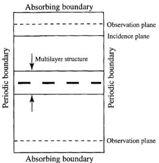
Figure 2-2: Cross section of the computational domain of FD-TD for periodic surfaces with absorbing boundary on top and bottom and periodic boundary at the sides.
2.1.3
Computational Domain
The computational domain is where the modeling of the filter is situated and the propagation and scattering are calculated. The cross section of the computational domain is shown in Figure 2-2. The top and bottom of the domain are terminated by absorbing boundaries and the sides are extended infinitely by imposing a periodic boundary condition. Inside the domain, the filter is in the middle of the computational column and the incidence plane where the incident plane wave is excited is above it. On top of the incidence plane, based on the "total-field/ scattered-field" formulation [14], only the scattered fields are calculated. The observation planes register the field quantities at every time step and through a temporal Fourier transform, the reflected and the transmitted fields at each sampled frequency can be calculated.
2.1.4
Modeling of Dielectrics and Conductors
Discontinuities of the propagation media in the computational domain are taken into consideration by different ways. In the presence of dielectric, the dielectric constant E will be the average value of the different dielectric materials that share the same edge. Differences in permeabilities require a special treatment [11, 14] due to the discontinuities introduced in the H fields. In the analysis of photonic crystal filters, the substrates and metals will assume the value of p,.
Conducting elements in the filters are modeled as perfect electrical conductors and have to satisfy the boundary condition that the tangential electric field is zero on the surfaces of the metal: El = 0. This can be implemented by assigning zeros to the tangential electric fields of the metal object at the end of each time step.
2.1.5
Absorbing Boundary Condition
In order to simulate an infinite space in a finite computational domain, the top and bottom end are terminated by an absorbing boundary. Perfectly Matched Layer, or PML [15] is used as the absorbing boundary condition. It functions by creating computational layers with increasing electric and magnetic losses at the interfaces and is usually backed by a conductor. The incident waves will be attenuated to a small value before they are reflected. The reflected waves will be further attenuated to a level that usually will not interfere with the calculation of the scattered fields. The full PML equations based on the decomposition of the field quantities can be found in [11]. The matching of the successive layers is ensured by the following relation:
0 E
FINITE-DIFFERENCE TIME-DOMAIN METHOD
H
~%
-J
---Figure 2-3: Periodic boundary condition. The field quantity outside the computa-tional cell can be updated via translacomputa-tional symmetry.
Hence the name perfectly matched layer. Given an incident angle of Oj, the reflection coefficient R of the PML can be expressed as:
-2 -") fz"'ax o(z)dz
R(Be) = e """ (2.8)
where Zmax is the total thickness of the absorbing layer and a(z) can be written as:
o(z) = omaz (Z)n
zmax
(2.9)
Thus the absorption will depend on the maximum loss Umax, the incidence angle O and the order n of the PML. As the incidence angle 62 approaches 900, the PML effectively becomes a conductor. And waves incident to the PML at grazing angles will be reflected and interfere with the observation of the scattered fields.
2.1.6
Periodic Boundary Condition
The physical structure consists of the periodic elements, the computational domain, however, is reduced to only a unit cell size. In order to simulate the repetitive cells, a periodic boundary condition is used. Based on the condition that the field distribution on the surface is periodic, it can be expressed as:
E(r, t) = H(r + pr, t) (2.10)
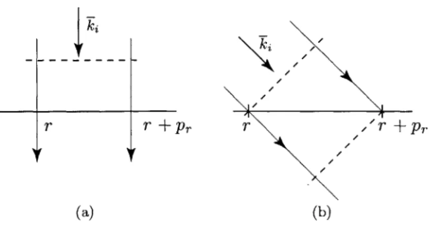
where p, is the periodicity of the structure. To apply this condition for the FD-TD code, first consider the electric field at the edge of the boundary (Figure 2-3). Take E. as an example. To calculate E. we need to know the value of Hz outside the boundary. But since the incident wave front is parallel to the surface (Figure 2-4a), by virtue of the periodic boundary condition, 7(r, t) = H(r + Pr, t). The periodicity is thus extended infinitely across the surface.
The situation is different for an obliquely incident wave (Figure 2-4b). The wave front is tilted and reach the surface at different times t. Since the validity of the operation (2.10) depend on the fact that the same phase front reaches the surface at the same time, the periodic boundary condition is no longer applicable in the case of oblique incidence. The updating process required an advanced field quantity and a
non-causal situation is encountered:
1(r, t,) = 7(r + pr, to + At) (2.11)
To preserve the periodic boundary condition, a variable transformation of the fields is needed, which leads to the FD-TD formulation for oblique incidence.
CHAPTER 2. FINITE-DIFFERENCE TIME-DOMAIN METHOD 24
(a) (b)
Figure 2-4: Comparison of wave front position between normal incidence and oblique incidence. Non-causal periodic boundary relation hinders the use of regular FD-TD for oblique incidence on periodic surfaces.
2.2
Oblique Incidence FD-TD
The oblique incidence formulation was first developed by Veysoglu [10], and Kao [11] derived the correct stability criteria and implemented them in the three-dimensional case. The method is based on adding a lateral phase shift to compensate the phase difference across the periodic surface so that the periodic boundary condition will causal again. In doing so, the Maxwell equations are changed to P -
Q
differential equations, where P andQ
are new field variable, replacing E and H.2.2.1
P
-
Q
Propagation Equations
Consider a plane wave at oblique incidence traveling in the -z direction (Figure 2-5) with a wavevector k = k
+
9ky - skz:Z
Y
x
Figure 2-5: Orientation of k-vector at oblique incidence.
Besides the dependence on z, the phase factor also depends on x and y. Define the lateral phase shift factor
e-ik -' e-ikx e-ikyy
with the lateral wavevector k, to compensate the contribution from k2 and ky. We can define new field variables P and
Q:
Q Hffeik1Te-ikj-feikzz (2.13)
Note that the lateral phase shift is removed and
P
andQ
propagate normal to the surface although the vectors themselves are not parallel to the surface. It is not a plane wave, and will satisfy Maxwell equation only with the appropriate transformation of variables.FINITE-DIFFERENCE TIME-DOMAIN METHOD
Rewriting Maxwell equations in the frequency domain for free space with P and
Q gives:
= wyoQ (2.14)
where 1' = - k1 is the
domain as:
wavevector of the P and Q. We can rewrite (2.14) in time
Q
VxQ A Va
t
A V X (2.15) whereA = , sin 0 cos
4
+9
sin 6 sin#5
(2.16)The equations (2.15) resemble the propagation of E and H in a bianisotropic medium [16]:
VxH
VxE = t(EoE
+
R )
=a
(po-H+
zE
at
(2.17)However, the P-Q system is dispersive, as the corresponding ( and ( are not contants but are dependent on the angles of incidence 0 and
#.
The subsequent difference equations are applied on the modified Yee's cell (Fig-ure 2-6) which can also be considered as a superposition of regular Yee cells. time stepping and the position of P and
Q
are shown in Figure 2-6.The 26 CH APT ER 2.
Ex
Q
+
i
xQ
=-WEoP =- EoP +at (
z 1I -pzIn
7(:ryp7
111I z I1 l'T -II4-y
rp 2 y -nx
Figure 2-6: Modified Yee's lattice .- I
1
Q+
Z-I
CHAPTER 2. FINITE-DIFFERENCE TIME-DOMAIN METHOD
2.2.2
Stability Criteria and Boundary Conditions
Stability Criteria
With the new P -
Q
system, the stability criterion is also changed. Based on Kao's calculation [11]:A > Vi
At -- v?/pe - sin2
{
sin cos $ + | sin sin$\ + j3vUpe - 2 sin2 0 (1- sin $ cos $|}
(2.18)
where vi is the phase velocity of the incident wave on the incidence plane. For the upper limit on the right side, y and e are chosen to be the least dense material in the computational domain. Figure 2-7 shows the ratio between A and cAt as a function
# (in degree, with 0 = 600)
A 250 200-150 -- 100-50 a' 0 10 20 30 40 50 60 70
0 (in degree, with 4 = 00)
Figure 2-7: Ratio between A and cAt vs. 0 and
p
of O and
p.
Along the azimuthal direction, this ratio has a four-fold symmetry and varies between minima (when the projection of k aligns with the x or y axis) and 28maxima (when the projection of ki is at 450 with the x or y axis). The same ratio
(N)
increase monotonically as the polar angle of incidence becomes larger. As 6O -> 900,-+ oo, and the time step At has to be infinitesimally small. On the other hand, as with the P - Q differential equation, the stability criterion reduces to the Courant's stability criterion as the propagation vector of the incident wave become normal.
Boundary Condition
The periodic boundary condition of the P -
Q
system is the same as in the case ofnormal incidence. Because of the finer grid, more field quantities are needed to be updated.
For the absorbing boundary conditions, the PML equations are changed in the same fashion as Maxwell equations. The lateral phase compensation is multiplied to the frequency domain equations before transforming back to the time domain.
The absorption of P and Q is similar to the normal incidence case. The simulations in this research are done with PML with 8 layers and the noise floor is below -100 dB.
Chapter 3
Simulation Results and Analysis
In this chapter, the simulation results and the analysis of the infrared bandstop filters are presented. Firstly, the calculated transmission coefficient of a 3D MDPC filter with 3D elements is compared to the experimental results, which demonstrate the reliability of using FD-TD as a design tool for IR filter. Secondly, the structure and the geometry of the proposed filter is presented It is composed of three layers of periodic metal patches embedded in a dielectric. The normal incidence transmission characteristics of the proposed filter are studied by varying the different geometric parameters. The optimal design is further evaluated at different incidence angles.
The effects of high permittivity and alignment are discussed.
3.1
Comparison between FD-TD and Experiment
in IR Band
Published results have shown good agreement between FD-TD and measurement in the GHz region [6]. To use FD-TD as a design tool, calculation is carried out to compare FD-TD and IR measurement results. The verification of the FD-TD
-* x S = 3.18 pm W =1.86pm e . p 2.1 d=1pm " 7---
---57
WF
El-
-II
h = 1m3D View of IR MDPC filter Cross Section
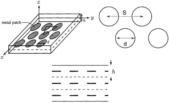
Figure 3-1: Geometry of the 3-D IR MDPC filter. Metallic parallelepipeds with square cross section is arranged in a face-center-cubic (100)-oriented crystal structure.
calculation for a 3D photonic crystal bandstop filter operating in the near infrared band is based on the published results in [4]. The geometry of the filter under study consists of metallic parallelepipeds with square cross section. These metal elements are embedded in a substrate of a planarizing polymer with a dielectric constant of
E, = 2.1. The elements are arranged such that they form the (100)-oriented face-centered cubic (fcc) crystal structure (Figure 3-1). The side of the square cross section is 1.86 pm, the center-to-center spacing is 3.18 pm and the thickness of the metal is 1 pm. The transmission of the filter was measured using a Fourier-transform spectrometer [4], with the effects of substrate and polymer compensated through a normalization measurement.
For the computer simulation, a normally incident field with a plane wave front and a Gaussian amplitude profile is used. The polarization of the incident electric field
Ej
is in the J direction. With FD-TD, the transmission coefficient of the i polarized wave is calculated. The transmission coefficients obtained are further attenuated by 5 dB to account for the experimental losses and the finite resistivity of the metal.CHAPTER 3. SIMULATION RESULTS AND ANALYSIS
0
. cj H-5
-10
-15
-20
0
1000
2000
Wavenumber (cm 1)3000
Figure 3-2: Comparison between FD-TD and experimental results of a 3D MDPC IR bandstop filter.
Figure 3-2. The solid line represents the experimental results and the dashed line shows the FD-TD results. Both display an onset of the stop band slightly below 1000 cm-'. However the calculated stop band has a smaller bandwidth and ends at approximately 1800 cm' instead of the measured 2500 cm- 1. The difference between the two may be due to dispersion of the dielectric, metal losses and dielectric losses which are not accounted for by FD-TD. Also the discretization error from the grid-ding process of FD-TD may have caused the discrepancy. The small features of the experimental results are also due to potential incomplete normalization measurement of the polymer substrate. The comparison demonstrates that FD-TD is theoretically applicable to predict the electromagnetic behavior of photonic crystal filters in the IR spectrum and establishes the reliability of FD-TD as a design tool in the IR region.
3.2
Parametric Study at Normal Incidence
In order to analyze the dual stop bands of a MDPC structure, a parametric study is carried out. The geometry of the filter under study is based on the design in [6] and has three layers (Figure 3-3). Each layer consists of periodic metal patches embedded in the middle of a dielectric. It was found that with the metal at the middle of the dielectric of each layer, the performance of the filter improves, as the top half layer of the dielectric acts as a superstrate. The whole structure consists of three such layers, which are aligned along the z-axis. The metal is assumed to be perfectly conducting and the dielectric constant of the substrate for the parametric study is 2.3.
z
S metal patch
A~gd x
Figure 3-3: Geometry of the design of one layer used in the parametric study and final design. Circular metal discs are arranged in a triangular grid, and are embedded in a dielectric substrate of E, = 2.1, 2.3.
CHAPTER 3. SIMULATION RESULTS AND ANALYSIS
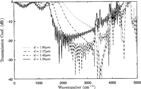
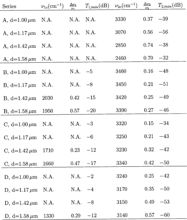
cosine function centered at 4000 cm 1 is used as the incident wave. Circular patches are discretized into 40 A-steps across the diameter to minimize the discretization error [11]. The spacing between the centers of the circular patches is kept at 2pm throughout the four series, and the diameter of the patches is varied from 1 pam to 1.58 pm which corresponds to different percentage filling of metal from 25 - 60 % in a unit cell in each series.
The results from the normal incidence simulation are shown in Figure 3-5 to 3-8. The y-axes of the graphs show the transmission coefficients in dB and the x-axes show the wave number in k = -, (cm 1).
0 -10 0 U 0 -20 0 EU -3 -40 L 0 1000 2000 3000 4000 Wavenumber (cm-1) 5000 Figure 3-4: Transmission S = 2 pm, d = 1.58 pm.
coefficients of bandstop filter with one layer of metal screen. 34
Figure 3-4 shows the transmission of one layer and only one major stop band is seen, which correlates with the separation between the elements. From Series A to D, the separation between the layers increases from 0.72 pm to 1.44 pm in four steps. In Figure 3-6 to 3-8, dual stop bands are observed. Although the structure is complicated, the formation of the stop bands can be explained. Two types of resonances are important in the formation of the stop bands. One is the resonance along the propagation direction, another one is the periodicity of the elements within the same layer.
Periodicity on the periodic surfaces contributes to the second stop band and the center frequency is determined by both the diameter of the circular patches and the spacing between the patches. The lattice constant, or the center to center separation S, determines the frequency at which the higher-order mode will start propagating. As the higher-order modes start propagating, the energy is diverted and creates a stop band in the fundamental mode. The patch itself acts as a reflector and as the filling percentage increases from 25% to 60%, the bandwidth of the second stop band can increase to over 50%.
The first stop band, on the other hand, only becomes apparent in the multilayer configuration and is not prominent for the case of one layer (Figure 3-4). The vertical resonance can be represented by a quarter-wave stack, because the metallic layer and the dielectric layer act as stack with alternating refractive indices. Since the metallic layer is not entirely filled (60 % maximum), the analogy is not complete. Nonetheless, there is a strong correlation between the two. Tabulated results (Table 3.1) show the shift of the resonance towards lower frequencies as the size of the patches increase.
1 keff =
CHAPTER 3. SIMULATION RESULTS AND ANALYSIS -10 20 -.4 --.--.. d =1.00pmI -- - d=1.17pm 11 -4 - - d = 1.42pm -30 - d = 1.58pm y -40 0 1000 2000 3000 4000 Wavenumber (cm~ ) 36 5000
Figure 3-5: Series A. Transmission coefficients of bandstop filters with three aligned layers of metallic screens. S = 2 pm, h = 0.72 pm.
0 -0 0 02 -10 -20 -30 -40 L 0 1000 2000 3000 4000 Wavenumber (cm-1) 5000
Figure 3-6: Series B. Transmission coefficients of bandstop filters with three aligned layers of metallic screens. S = 2 ym, h = 0.96 ym.
0 0 0 0e -10 -20 -30 -40 L-0 1000 2000 3000 4000 Wavenumber (cm- 1 )
Figure 3-7: Series C. Transmission coefficients of bandstop filters with three aligned layers of metallic screens. S = 2 pm, h = 1.14 ym.
0 -10 0 0 -20 -30 -40 L 0 1000 2000 3000 4000 Wavenumber (cm- 1)
Figure 3-8: Series D. Transmission coefficients of bandstop filters with three aligned layers of metallic screens. S = 2 pm, h = 1.44 ym.
5000
CHAPTER 3. SIMULATION RESULTS AND ANALYSIS h 0.72 pm 0.96pm 1.14 pm 1.44 pm keff (calculated) 2289 cm 1 1717 cm-1 1479 cm-1 1441 cm 1
Table 3.1: Resonance frequency based on calculation.
an ultra wide stop band with a percentage bandwidth in excess of 70%.
To show the performance quantitatively, the relative bandwidth of each of the stop bands and the minima of the transmission coefficients are tabulated in Table 3.2.
v2c(cm-1) Av2 T2,min(dB) Series A, d=1.00 pm. A, d=1.17pm A, d=1.42pm B, d=1.58tm B, d=1.00pm B, d=1.17[tm B, d=1.42pm B, d=1.58pm C, d=1.00pm C, d= 1. 17 pm C, d=1.42 pm C, d=1.58 pm D, d=1.00 pm D, d=1.17 pm D, d=1.42[pm D, d=1.58 pm, N.A. N.A. N.A. N.A. N.A. N.A. 2030 1950 N.A. N.A. 1710 1660 N.A. N.A. N.A. 1330 N.A. N.A. N.A. N.A. N.A. N.A. 0.42 0.57 N.A. N.A. 0.23 0.47 N.A. N.A. N.A. 0.29 N.A. N.A. N.A. N.A. -5 -8 -15 -20 -3 -6 -12 -17 -2 -4 -8 -12 3330 3070 2850 2460 3460 3450 3420 3390 3320 3250 3230 3340 3240 3170 3150 3140 0.37 0.56 0.74 0.70 0.16 0.21 0.25 0.27 0.15 0.21 0.32 0.42 0.25 0.35 0.49 0.57
Table 3.2: Relative bandwidth and minimum transmission coefficients of the bandstop filters (parametric study).
-39 -56 -38 -32 -48 -51 -49 -46 -34 -43 -42 -50 -42 -50 -53 -60
CHAPTER 3. SIMULATION RESULTS AND ANALYSIS
3.3
Effects of Metal Thickness and Dielectric
Con-stant of Substrate
3.3.1
Metal with Finite Thickness
Instead of the 3D element shown in Figure 3-1, the new IR filter features thin metal patches instead. With thin metal, the choice of dielectric substrate is wider as the substrate will not be confined to a planarizing one. This is because the deposition of a thinner metal layer results in a smoother surface. As shown later in this section, the permittivities of the dielectric substrate has a direct effect on the angular dispersion properties of the filter. The simulated structure consists of periodic square patches in a square grid. The sides of the patches are of length 3 cm and the sides of the grids are 6 cm. A metal patch with no thickness is simulated with only E, and Ey to model the patch. A patch with finite thickness is modeled here by having an aspect ratio between thickness and width of 1: 10 and contains the value of
E,
as well. The result is shown in Figure 3-9.The changes in bandwidth and the position of resonance are very small between the two. Thus the calculation of the designs are based on infinitely thin metal patches.
3.3.2
Dielectric with High Permittivity
As the filter is required to perform its function over a wide range of angles the angular performance is very important. An analysis has been carried out regarding the choice of the dielectric constant of the substrate and superstrate and the trade off between high and low dielectric constant is discussed. Figure 3-10 shows an incident plane wave at O6 = 450 and the output angles for dielectrics with different permittivity are Ot = 18.8' and t2 = 29'. It is seen that as the dielectric constant increases, the filter 40
0 -10 20 C12 PJ 0 1 2 3 4 5 6 7 8 9 10 Frequency (GHz)
Figure 3-9: Infinitely thin metal vs. metal with finite thickness.
will be subjected to less angular dispersion. Oblique incidence calculations are carried out for the previous structure. The dielectric constants for comparison are chosen to be 2.3 and 4.8. Figure 3-11 and Figure 3-12 show the distortion of the shape of the stop band as the angle of incidence increase. While a higher index preserves the stop band characteristics over a wider range of angles, it also makes the fabrication of the MDPC more difficult. Higher dielectric constants also introduce higher out-of-band losses.
3.4
Optimal Design of Filter and Performance at
Oblique Incidence
This section presents the final design of the IR filters which have a substrate with a dielectric constant of 2.1. The spacing between the elements is 3.2 yum, the separation
CHAPTER 3. SIMULATION RESULTS AND ANALYSIS
t = 18.80 for Er = 4.8 Ot2 = 290 for er = 2.1
Figure 3-10: Internal angles for superstrates with different permittivities.
between the layers is 2.7 pm and the diameter of the disk is 2.6 pm.
c, = 2.1
S = 3.2 pm
h = 2.7 Am
d = 2.6 pm
Two implementations are analyzed, one of them uses aligned metal patches and the other one uses a face-center-cubic structure. The structures have a six-fold symmetry along the azimuthal direction. The azimuthal angles
4
= 00 and#
= 90' represent the best and worst cases as the azimuthal angles varies and the transmission coefficientsat different polar angles are calculated for different polarization (TE and TM). It is found that the alignment of the thin metallic patches does not change the properties of the stop bands very much.
0 0 U 0 ~I2 -10 -20 -30 -40 L-0 1000 2000 3000 4000 Wavenumber (cm-1) 5000
Figure 3-11: Transmission characteristics with substrate having c, = 2.3.
0 -4 0 ce -10 -20 -30 -40 ' 0 1000 2000 3000 4000 Wavenumber (cm- 1 ) 5000
CHAPTER 3. SIMULATION RESULTS AND ANALYSIS
3.4.1
Aligned Structure
Figure 3-14 and Figure 3-15 show the transmission characteristics of the filter upon TE and TM incidence with azimuthal angle
#
= 00. We can see that the dual stop band for the TE incidence persists from 0' to 600. The upper edge of the low frequency band is more susceptible to the angular dispersion, and it shifts up the spectrum as the polar angle increases. This can be due to the low dielectric constant of the substrate and also the blue shift because of the vertically aligned stack, analogous to a dielectric mirror. For the second band, there is a same tendency for the upper edge to shift up the spectrum. For TM incidence, there is a significant degradation of performance for0000
0
)
0 00
x
Figure 3-13: Azimuthal angle of incidence
#
with respect to the filter.the second band. This might be due to the thin metallic elements which are incapable of scattering the incident EM wave with the polarization perpendicular to the metal at large polar angles. For the first resonance, both the lower edge and upper edge of the band experience a blue shift as the incident angle goes higher. The quantitative performance of the filter is presented in Table 3.3, which show the relative bandwidth and the minima of the transmission spectrum.
Figure 3-16 and Figure 3-17 show the results of the transmission characteristics of the filter upon TE and TM incidence with azimuthal angle
#
= 90'. The first stop 44band, for both TE and TM exhibit similar characteristics as when the azimuthal angle of incidence is
#
= 00. The second stop band has different characteristics because of the azimuthal asymmetry. Consequently, the stop band is only partial and subjected to variation upon changing the polar angle of incidence.In conclusion, for the aligned structure, with TE incidence, the stop band trans-mission is below -10 dB for 8 - 12 tm and the stop band at higher frequencies has a partial stop band from 3 - 5 pm.
CHAPTER 3. SIMULATION RESULTS AND ANALYSIS 0 0 Qe 04 -10 -20 -30 -40 'I - .I .. k I I I-0 500 1000 1500 2000 2500 3000 Wavenumber (cm- 1)
Figure 3-14: Transmission coefficient for TE incidence, 0 = 00 - 600,
#
= 00.'0 0 0e p -10 -20 -30 -40 1 1. 1"i-0 500 1000 1500 2000 2500 3000 Wavenumber (cm 1)
Figure 3-15: Transmission coefficient for TM incidence, 0 = 00 - 600,
4
= 0'.-10 -20 -30 -40 0 500 1000 1500 2000 2500 3000 Wavenumber (cm- 1 )
Figure 3-16: Transmission coefficient for TE incidence, 6 = 0' - 600,
#
= 90'.-o 12 -10 -20 -30 -40 " 0 500 1000 1500 2000 2500 3000 Wavenumber (cm-1)
CHAPTER 3. SIMULATION RESULTS AND ANALYSIS
Series vic(cm- 1) ' Ti,min(dB) v2c(cm-1) "V2 T2,min(dB)
TE 0 = 0= 0' 1035 0.45 -15 2210 0.51 -52 TE 9 = 22.50 ' = 00 1065 0.48 -16 2215 0.24 -44 TE 0 = 450 = 00 1150 0.57 -20 2320 0.29 -46 TE 9 = 600 = 0 1035 0.75 -25 2340 0.32 -42 TM 9 = 00 = 00 1030 0.47 -16 2185 0.50 -70 TM 9 = 22.5
4
= 0' 1080 0.46 -16 2155 0.50 -45TM 0 = 45' #= 0* 1220 0.49 -19 N.A. N.A. N.A.
TM 9 = 600 = 0' 1430 0.60 -25 N.A. N.A. N.A.
TE 9 = 00 = 90' 1035 0.45 -16 2180 0.49 -60
TE 0 = 22.50 = 90* 1060 0.49 -17 2365 0.60 -46
TE 9 = 450 = 90' 1150 0.57 -20 2025 0.17 -33
TE 9 = 600 = 90' 1200 0.67 -20 N.A. N.A. N.A.
TM 9 = 0 # = 90 1025 0.44 -15 2225 0.52 -55
TM 9 = 22.50 = 90' 1080 0.44 -15 1975 0.35 -37
TM 0 = 45' #= 900 1225 0.45 -15 N.A. N.A. N.A.
TM 9 = 600 = 900 1275 0.43 -25 N.A. N.A. N.A.
Table 3.3: Relative bandwidths of the dual stop bands at different incident angles (aligned structure).
3.4.2
Face-Center-Cubic Structures
Figure 3-18: Relative position of the metal patches at different layers for a face-center-cubic structure.
In this section a second implementation of the filter is presented. In the aligned design, the metal patches are stacked on top of each other, hence the performance for different azimuthal and polar angle of incidence may degrade as the cross section of metal as seen by the incident wave decreases.
For the face-center-cubic
(fcc)
case, the metal patches are arranged such that between each layer there is an offset. The vertical period comprises three layers 1,2 and 3. The relative position of the labeled metal patches is shown in Figure 3-18, which indicate the center position of the patches. This configuration is expected to have a more consistent performance for different azimuthal angles of incidence. The unit cells used are shown in Figure 3-19.
For TE incident with
#
= 00, the pass band up to 12 pm has a transmission20
CHAPTER 3. SIMULATION RESULTS AND ANALYSIS
coefficient of less than -3 dB in the case of normal incidence and the stop band from 8-12 pum has a transmission coefficient of less than -15 dB. Due to the offset between layers, the lower edge of the second stop band is not as steep as the aligned one.
For TM incidence with
#
= 00, no significant improvement is observed. Similar to the aligned case, the second stop band degrades very fast and the transmission coefficient starts oscillating above the -10 dB level as the polar angle is off normal. Both TE and TM at#
= 90' incidence show an improvement over the aligned structure. The second stop band appears to be more stable over a wider range of polar angles. Overall, the face-center-cubic structure offers slightly more consistent transmission characteristics along the azimuthal direction.For comparison, the center frequencies, relative bandwidth, minimum transmission coefficient in (dB) for the face-center-cubic implementations are tabulated in Table
3.4.
-o 0 -10 -20 -30 -40 0 500 1000 1500 2000 2500 3000 Wavenumber (cm-1)
Figure 3-20: Transmission coefficient (fcc) for TE incidence, 0 = 0 - 60',
#
= 0'.-o 0 U 0 Ci) -10 -20 -30 -40 11 . 1 7* II ! 0 500 1000 1500 2000 2500 3000 Wavenumber (cm-1)
CHAPTER 3. SIMULATION RESULTS AND ANALYSIS -10 0 -20 0 ~-30 -40' 0 500 1000 1500 2000 2500 3000 Wavenumber (cm-1)
Figure 3-22: Transmission coefficient (fcc) for TE incidence, 0 = 0' - 60', # = 90'.
0 -o 0 U 0 U) U) -10 -20 -30 -40' 0 500 1000 1500 2000 2500 3000 Wavenumber (cm -1)
Figure 3-23: Transmission coefficient (fcc) for TM incidence, 6 = 0' - 600,
#
= 90'.Series TE6= 0 TE6= 2 TE6 = 4 TE 6= 6 TM 6 = TM 6 = TM 6 = 0 2.50 50 00 00 22.50 450 q5= 00 00 00 00 00 00 0 0 vic(cm- 1) 1040 1070 1170 1170 1040 1070 1215 AV, 0.46 0.47 0.56 0.60 0.46 0.47 0.47 Ti,min(dB) -15 -16 -18 -22 -15 -15 -18 2275 2275 2220 2520 2275 2350 N.A. v2c(cm- 1) A 2 0.55 0.24 0.29 0.38 0.55 0.13 N.A. -52 -40 -44 -33 -67 -35 N.A. A
TM
0
= 600 p = U 143U U.5 -U iN.A. iN.IA. iN..TE 6 = 00 = 900 1040 0.46 -15 2275 0.55 -67 TE 6 = 22.50 = 90' 1065 0.50 -16 2675 0.32 -48 TE 6 450 # = 900 1160 0.62 -18 2875 0.43 -37 TE 0 = 600 = 900 1200 0.67 -22 2825 0.48 -33 TM 6 = 00 = 90' 1040 0.46 -15 2275 0.55 -52 TM 6 = 22.50 = 90 1085 0.43 -15 2340 0.31 -42 TM 6 = 450 = 90 1225 0.45 -17 2900 0.40 -48 TM 6 = 600 = 90 1270 0.39 -20 2580 0.28 -44
Table 3.4: Relative bandwidths of the dual stop bands at different incidence angles (fec structure).
Chapter 4
Hybrid Method for Multilayer
Analysis
In this chapter, the formulation of a hybrid method for treating multilayer structures is presented. The transfer matrix method is used in conjunction with the FD-TD calculation.
The transfer matrix method has been applied to many circuit and transmission line problems. Application to the cascade of metallic periodic screens has been discussed in [17, 18, 19]. In [20], computation of the scattered fields from free-standing metal patches was computed by frequency domain methods, combined with the matrix formulation given in [17], where the cascade of a metal screen with different dielectric slabs was analyzed. Cascading of grating screens and formulation for shifted units was presented by Hall [18]. The generalized scattering matrix [19] takes into account higher-order modes and evanescent coupling between closely spaced layers. Cascading of multiple metal screens with dielectric slabs was also analyzed.
The elements of the scattering matrix consist of the forward scattering and the backward scattering coefficients of different modes and are usually calculated by