Automatic Application-Specific Optimizations under
FPGA Memory Abstractions
by
Hsin-Jung Yang
B.S., National Taiwan University (2010) S.M., Massachusetts Institute of Technology (2012)
Submitted to the
Department of Electrical Engineering and Computer Science
in partial fulfillment of the requirements for the degree of
Doctor of Philosophy
in Electrical Engineering and Computer Science
at the Massachusetts Institute of Technology
June 2017
C
Massachusetts Institute of Technology 2017
All Rights Reserved.
A uthor ...
Signature redacted
OF TECHNQLQGY ,
JUN 2
3
Z017
LIBRARIES
AFkCHIVES
Department of Electrical Engineering a d Computer Science
7!
AMay 12, 2017
Signature redacted
Certified by
. ... . .. . .. .Srinivas Devadas
Professor of Electrical Engineering and Computer Science
Thesis Supervisor
Certified
by...
Signature
redacted
...
Joel Emer
Professor of Electrical Engineering and Computer Science
Thesis Supervisor
Signature redacted ...
Accepted by .
/ I64i A. Kolodziejski
Automatic Application-Specific Optimizations under FPGA Memory
Abstractions
by
Hsin-Jung Yang
Submitted to the Department of Electrical Engineering and Computer Science on May 12, 2017, in partial fulfillment of the
requirements for the degree of
Doctor of Philosophy in Electrical Engineering and Computer Science
Abstract
FPGA-based accelerators have great potential to achieve better performance and energy-efficiency compared to general-purpose solutions because FPGAs permit the tailoring of hardware to a particular application. This hardware malleability extends to FPGA memory systems: unlike conventional processors, in which the memory system is fixed at design time, cache algorithms and network topologies of FPGA memory hierarchies may all be tuned to improve application performance. As FPGAs have grown in size and capacity, FPGA physical memories have become richer and more diverse in order to support the increased computational capacity of FPGA fabrics. Using these resources, and using them well, has become commensurately more difficult, especially in the context of legacy designs ported from smaller, simpler FPGA systems. This growing complexity necessitates automated build procedures that can make good use of memory resources by performing resource-aware, application-specific optimizations.
In this thesis, we leverage the freedom of abstraction to build program-optimized memory hierarchies on behalf of the user, making FPGA programming easier and more efficient. To enable better generation of these memory hierarchies, we first provide a set of easy-to-use memory abstractions and perform several optimization mechanisms under the abstractions to construct various memory building blocks with different performance and cost tradeoffs. Then, we introduce a program introspection mechanism to analyze the runtime memory access characteristics of a given application. Finally, we propose a feedback-directed memory compiler that automatically synthesizes customized memory hierarchies tailored for different FPGA applications and platforms, enabling user programs to take advantage of the increasing memory capabilities of modern FPGAs.
Thesis Supervisor: Srinivas Devadas
Title: Professor of Electrical Engineering and Computer Science
Acknowledgments
I would like to acknowledge the support of many people who made this thesis possible. First and foremost, I would like to express my sincere gratitude to my advisors, Professor Srinivas Devadas and Professor Joel Emer, for their encouragement and support through-out these years. Srini's enthusiasm for research is contagious and I am deeply grateful for the freedom he has given me to pursue the research that interests me most. I especially want to thank Joel, whom I have worked closely with through my PhD study. Being a great mentor and role model, Joel has always been patient and supportive. I appreciate the invaluable research guidance and thoughtful career advice he has given me as well as all the life stories he has shared with me. I would also like to thank my thesis committee member, Professor Daniel Sanchez, for providing insightful feedback and constructive suggestions to improve the quality of this thesis.
I want to extend my gratitude to my collaborators, Elliott Fleming and Michael Adler from Intel, Felix Winterstein from Imperial College London, and Annie Chen from MIT. Working with them has been a pleasant experience. Without them, I would not be able to complete my thesis projects. I would like to profoundly thank Elliott and Michael for their immeasurable help in brainstorming research ideas, conducting evaluation experiments, and writing research papers. Through collaboration and weekly phone meetings with them (as well as countless Skype conversations with Elliott), I have learned a lot in the field of reconfigurable computing and improved my paper writing and presentation skills. I am also grateful for the successful and productive collaboration with Felix. Felix have developed many high-level synthesis applications that are important benchmarks for performance evaluation. I want to thank Annie, who has also been a good friend of mine for 14 years, for helping me formulate optimization problems and develop algorithms presented in the thesis.
I am thankful to the members of the Hornet group for creating a great working environment. I appreciate the stimulating conversations and helpful discussions with them. Special thanks to Ilia Lebedev, who has helped me fix my FPGA evaluation board
Many thanks go to all of my friends who have supported me through the ups and
downs of my PhD journey and made my time at MIT enjoyable. Thanks Amy Chen for
providing a lot of help in research and life, including sharing her beautifully formatted
thesis template with me. Thanks Lixin Sun and Annie Chen for sharing wonderful times
with me as well as their tasty homemade meals and desserts. I would also like to thank
Chern Chuang for encouraging me, cheering me up, and always being there for me during
the past three years. Finally, I am eternally grateful to my parents for their unconditional
love and full support throughout my life.
Contents
Abstract 111Acknowledgments
v
Contents
vii
List of Figures...
xi
List of Tables ...
...
...
..
xv
List of Algorithms ...
...
xvii1
Introduction
1
1.1
Thesis Contribution ....
...
...
...
7
1.2
Thesis Organization ..
...
... ...
9
2
Background
11
2.1
The LEAP FPGA Operating System . . . .
11
2.1.1
Model of Computation . . . .
12
2.1.2
LEAP Private Memory . . . .
15
2.1.3
LEAP Compilation . . . .
17
2.2
Extending LEAP Memories to HLS Applications . . . .
18
2.3
FPGA Platforms and Workloads for Evaluation . . . .
20
2.3.2
HLS-Compiled Applications ...
24
2.3.3
FPGA Platforms . . . .
26
3
Related Work
29
3.1
FPGA High-Level Programming Environments . . . .
29
3.2
FPGA High-Level Synthesis Tools . . . .
30
3.3
FPGA Memory Abstractions . . . .
32
3.4
Managing Coherency and Synchronization on FPGA . . . .
34
3.5
Memory Optimizations . . . .
35
3.5.1
Memory Optimizations in Processors . . . .
36
3.5.2
Memory Network Optimizations in Embedded SoCs . . . .
39
3.5.3
Memory Optimizations on FPGAs . . . .
40
4 Shared Memory Abstraction
43
4.1
LEAP Coherent Memory . . . .
45
4.1.1
Coherent Memory Interface . . . .
46
4.1.2
Coherence Protocol . . . .
47
4.1.3
Coherent Memory Architecture . . . .
49
4.1.4
Coherent Memory Client Microarchitecture . . . .
50
4.1.5
Coherence Controller Microarchitecture . . . .
52
4.1.6
Deadlock Freedom . . . .
53
4.1.7
Memory Consistency . . . .
54
4.2
Coherent Cache Network Optimization . . . .
55
4.3
Synchronization Primitives . . . .
59
4.3.1
Lock Service . . . .
59
4.3.2
Barrier Service . . . .
60
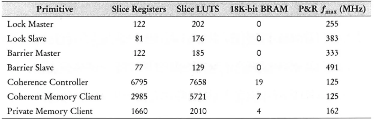
4.4 Evaluation . . . .
62
4.4.1
Coherent Memory Service . . . .
62
4.4.2
Synchronization Service . . . .
66
4.4.3
Implementation Area . . . .
67
4.5
Sum m ary . . . .
68
vill
5 Cache Optimizations
71
5.1
Cache Prefetching . . . .
72
5.1.1
Prefetching In FPGAs . . . .
72
5.1.2
Prefetching Microarchitecture . . . .
74
5.1.3
Evaluation . . . .
78
5.2
Scalable Caches . . . .
83
5.2.1
On-chip Shared Cache . . . .
84
5.2.2
Cache Scalability . . . .
87
5.2.3
Non-power-of-two Caches . . . .
88
5.2.4
Design Tradeoff . . . .
90
5.2.5
Compile Time Optimization
. . . .
91
5.2.6
Evaluation . . . .
93
5.3
Summary . . . .
105
6 Service Communication Abstraction
107
6.1
Motivating Example . . . 108
6.2
Communication Abstraction . . . 109
6.3
Network Topologies . . . .
111
7 LEAP Memory Compiler
115
7.1
Compiler Overview
. . . .
117
7.2
Construction of Optimized Cache Networks . . . 120
7.2.1
Resource-Aware Program-Optimized Memory Partitioning
.
. .
121
7.2.2
Cache Network Profiler . . . 125
7.2.3
Program-Optimized Tree Networks . . . .
128
7.3
Evaluation . . . .
132
7.3.1
Cache Network Partitioning . . . .
133
7.3.2
Program-Optimized Cache Networks . . . .
142
8 Conclusion
153
8.1
Thesis Summary ...
153
8.2
Future Work ...
156
Bibliography
159
List of Figures
1-1
An example of a program-optimized FPGA memory hierarchy. . . . . .
8
2-1
A pair of modules connected by a latency-insensitive channel. The send
and receive endpoints with the same channel name ("AtoB") are matched
during compilation. . . . .
13
2-2
LEAP private memory interface . . . .
15
2-3
An example of LEAP private memory hierarchy. . . . .
16
2-4
LEAP compilation flow. . . . .
17
2-5
Automating the integration of HLS applications and LEAP-generated
platform s. . . . .
20
2-6
A simple nested loop that models heat transfer from time 0 to time T on
an M x N grid. Co, C, C, are constants related to thermal diffusivity.
23
4-1
The LEAP coherent memory interface extended from the private memory
interface with extensions highlighted. . . . .
46
4-2
Coherent memory architecture. . . . .
49
4-3
Coherent cache microarchitecture. . . . .
51
4-4
Coherence controller microarchitecture . . . .
52
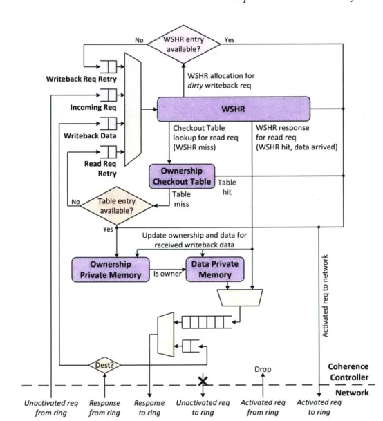
4-6
A walkthrough example of coherency management in a-multi-controller
system .
. . . .
57
4-7 A lock service walkthrough example. . . . .
61
4-8
LEAP memory hit latency comparison. . . . .
63
4-9
LEAP memory throughput comparison. . . . .
63
4-10 Performance comparison of different coherent memory configurations
for heat with a various number of worker engines. . . . .
64
4-11 Performance comparison of coherent memories with single and dual
coherence controllers when running heat at various frame sizes with 16
worker engines. . . . .
64
5-1
The microarchitecture of the LEAP private memory client's private cache
with prefetching logic. Our augmentations are highlighted.
. . . .
74
5-2
Prefetcher performance results normalized to a non-prefetched
implemen-tation. . . . .
80
5-3
Prefetch result analysis for MMM.
. . . .
81
5-4
The extended LEAP private memory hierarchy, including scalable BRAM
caches and a shared on-chip cache. Our modifications are highlighted. . . 855-5
Set associative cache microarchitecture. . . . .
86
5-6
BRAM store implementation option. . . . .
88
5-7
Cache indexing mechanisms for power-of-two and non-power-of-two caches. 89
5-8
An example of a LEAP program built with the two-phase compilation flow. 92
5-9
Li cache performance with various microarchitectures. . . . .
95
5-10 Performance metrics
for
HAsim with various cache configurations. . . . 975-11 Performance comparison
for heat
with various cache configurations. . .. 995-12 Performance comparison for HLS kernels with various Li cache sizes.
Results are normalized to the performance of the smallest monolithic cache. 100
5-13 Performance comparison of the banked cache against the monolithic cache
for various benchmarks built with maximal Li cache sizes. . . . .
101
5-14 Implementation space of L2 caches. . . . .
101
xii5-15 Relative throughput gain
for
memperf . . . 1026-1
The abstract interfaces of service connections.
. . . .
110
6-2
Communication abstraction for centralized services. . . . .
111
6-3
Examples of compiler-generated network topologies. . . . 112
7-1
Extended LEAP compilation flow with our extensions highlighted in blue. 118
7-2
Program instrumentation built with the LEAP statistics collection service. 119
7-3
LEAP private memory system with a partitioned cache network. . . . .
121
7-4
LEAP private memory interleaver logic microarchitecture. . . . 124
7-5
LEAP dynamic parameter service. . . . 126
7-6
An application-specific network profiler with instrumentation logic and
latency FIFOs inserted at each memory client. . . . .
127
7-7
Performance of memperf for various LEAP memory systems. . . . .
134
7-8
Performance of mergesort on 256 kilo-entry lists with different memory
network configurations and a various number of parallel sorters, averaged
over all the sorters and normalized to the baseline implementations. . . . 1377-9
Performance of heat on a 1-mega-entry array with various memory
net-work configurations, normalized to the baseline implementations with a
single coherence controller . . . .
137
7-10 Performance of filter and reflect-tree with various memory network
config-urations, normalized to the baseline implementations. . . . .
138
7-11 Performance of best-achieved performance solutions for 8-bit heat and
mergesort with various platform configurations, normalized to
single-VC707 solutions. . . . .
. 141
7-12 Latency sensitivity of memory clients infilter. . . . . 1447-13 Simulated performance of filter with various tree construction algorithms. 145
7-14 Performance comparison of various network configurations for
single-program applications, normalized to the actual baseline implementations. 146
7-15 Performance comparison of various network configurations for the
mergesort-filter application. . . . 148
7-16 Performance comparison for the heat-filter application. . . . . 149
List of Tables
2-1
FPGA platforms for evaluation. . . . .
26
4-1
Shared queue test runtime result . . . .
66
4-2
Throughput comparison of barrier services. . . . .
66
4-3
FPGA resource utilization and maximum frequency of shared memory
prim itives. . . . .
67
4-4
Normalized area of coherent caches with various configurations.
. . . .
68
5-1
Structural and performance metrics for board-level memories on FPGA
evaluation platforms, as measured at the memory controller. . . . .
78
5-2
FPGA resource utilization and maximum frequency of prefetching logic.
82
5-3
Post-place-and-route results for applications with different cache sizes. . .
94
5-4 L2 cache performance gainfor
merger. . . . . 1035-5
Power and energy measurements for HLS applications'. . ...
104
7-1
FPGA resource utilization for memory system components. . . . .
135
7-2
Resource utilization for baseline and best performing memory
configura-tions. . . . 136
7-3
Resource utilization for various network primitives. . . . 143
7-4
Resource utilization for the cache network infilter. . . . 143
List of Algorithms
6-1
Arbiter with bandwidth control. . . . .
113
7-1
Private cache network partitioning. . . . .
123
7-2
Construct a minimum weight tree using DP. . . . . .
...
. . . .
131
Introduction
Field-programmable gate arrays (FPGAs), which were originally used for
application-specific integrated circuit (ASIC) prototyping and emulation, have grown in capacity
and become increasingly popular as accelerators in both academia and industry [15, 34,
73,
77,
78, 81, 90]. Massive parallelism and specialization make FPGAs attractive to
improve the performance and power efficiency of applications that conventionally run on
general-purpose machines
[36,
55, 89]. To achieve high performance and efficiency, FPGA
programmers have traditionally utilized low-level primitives and hardware description
languages (HDLs), such as VHDL and Verilog, manually managing fine-grained
paral-lelism and explicitly customizing their implementation both to the target application and
to the target platform. This approach, while effective, has made FPGA programs difficult
to write, limiting both developer productivity and portability across FPGA platforms.
The difficulty of designing hardware at register transfer level (RTL) has also inhibited the
wide adoption of FPGA-based solutions.
To reduce programming effort and shorten development time, recent work has focused
on raising the level of abstraction available to FPGA programmers. Several higher-level
programming languages, such as Bluespec [12], Lime [8], and Chisel [9], as well as
associated compiler frameworks that automate the transformation from these languages
to RTL implementations have been proposed. Numerous C-to-hardware compilers,
including Xilinx Vivado High-Level Synthesis [94], ROCCC [93], LegUp [13], Catapult
C [14], Impulse C [47], and Cadence Stratus High-Level Synthesis [86], have been
Chapter 1. Introduction
developed to extract parallelism from C/C+ +/SystemC source codes and automatically map software kernels to RTL specifications, making FPGA programming easier and more
acceptable for software programmers.
In addition to these high-level synthesis (HLS) tools, another class of work has added new programming primitives to existing HDLs, enabling HDL programmers to concisely express program behavior at a higher level than register transfers. Examples of higher-level constructs include communication services, to software [57, 85], within the FPGA [76], and between FPGAs [32], as well as memory abstractions [3, 19, 57]. These primitives, which abstract away vendor-specific interfaces and resources, can be configured and reused for various applications across different FPGA platforms.
High-level abstractions provide clearly-defined, generic interfaces that separate the user program from underlying infrastructure implementations, such as memory, com-munication, and other ancillary services. FPGA programmers can therefore concentrate on algorithm design while programming against fixed interface layers. These interface layers allow users to write portable programs, which can run on different platforms without changes to the application code. Underneath the interfaces, low-level platform implementation details are handled by a combination of compilers and system devel-opers. Such abstractions enable the platform to be optimized separately, improving program performance without perturbing the original user design. However, there is rarely a globally optimal platform design strategy for different applications. High-level abstractions and productivity may come at the expense of performance, resulting in a performance gap between a generated system and a manually optimized design. To construct high-performance designs while maintaining high productivity, it is essential to develop algorithms and tools that optimize platform service implementations in an application-specific manner on behalf of programmers.
This thesis primarily focuses on one aspect of platform optimizations: FPGA memory systems. In both conventional processors and FPGAs, the memory system is critical to overall program performance for a broad class of applications. The memory system on a specific conventional processor is fixed and therefore a compromise based on a set of expected workloads to achieve the best average performance. In contrast, cache
algorithms or the memory hierarchies on FPGAs can be tailored for different applications. For example, a well-pipelined, bandwidth-intensive program might not need a cache at all, while a latency-sensitive program, like a soft-processor or a graph algorithm implementation, might prefer a fast first-level cache. Building customized memory systems to achieve high program performance involves exploring a large design space. Therefore, it is important to have an automated build procedure that facilitates this exploration process.
In addition, FPGA programs rarely consume all the resources available on a given FPGA, partly due to design difficulty such as cache scalability and partly due to design reuse. Existing platform abstractions enable designs to be ported across FPGAs, but a large amount of resources may be left unused when an algorithm design targeting an older, smaller FPGA is ported to a newer, larger FPGA. Producing efficient and portable FPGA designs requires resource-aware platform optimizations that exploit the unused resources to improve performance. For example, a resource-aware memory compiler might utilize spare resources to build prefetching logic or to increase the size of the on-chip caches.
Automatic, resource-aware optimizations are especially important for utilizing coarse-grained resources, like board-level memories, which have traditionally been difficult to integrate at design time. As the availability of more transistors makes it feasible to build larger, bandwidth-hungry designs as well as the memory controllers necessary to feed them, modern FPGA boards have begun to include multiple dynamic random-access memories (DRAMs) [68, 104]. Moreover, the number of memory controllers is increasing rapidly as vendors move to harden memory interfaces [2, 68]. To improve performance, it is critical for a memory compiler to make good use of these increasingly rich and varied memory resources without drastically increasing the design burden.
This thesis aims to automatically construct an optimized memory system tailored for a given FPGA application on a particular platform. To achieve this goal, the key requirements are memory abstractions, optimizations performed under the abstraction, and an automated build procedure that selects and implements the best optimizations. First, we need a set of easy-to-use memory abstractions to support a wide variety of applications, including programs written in RTL and in high-level languages (such as
Chapter 1. Introduction
C/C + + or domain-specific languages). These memory abstractions separate the user program from details of the memory system implementation, thus enabling changes in the memory system without requiring modifications in the user code. Second, we need various optimization mechanisms that are performed under the abstraction to construct a rich set of memory building blocks with different performance and cost tradeoffs. Finally, we need a build procedure that automatically composes an application-specific hierarchy from these memory building blocks. This build procedure includes program introspection, which characterizes the program's runtime memory access behavior. The introspection results, together with program resource utilization, are used by a feedback-directed compiler to guide the selection of optimal memory building blocks and the implementation of an optimized memory hierarchy tailored for the target application and platform.
Recent research has provided a number of abstract memory interfaces that hide memory implementation details from application designers and enable compilers to assist in the construction of application-specific memory systems. For example, the Connected RAM (CoRAM) [19] architecture defines an application environment that separates computation from memory management. CoRAM memory accesses are managed by control threads that fetch data from off-chip memories to on-chip buffers using a C-like language. LEAP (Latency-insensitive Environment for Application Programming) private memories [3] provide a memory abstraction with a simple request-response-based interface and manage a memory hierarchy extending from on-chip block RAMs (BRAMs) to the host processor's memory. We adopt the LEAP private memory abstraction as the base of this thesis work, because it provides a simple user interface, while giving us enough flexibility to construct a diverse set of memory hierarchies.
To make application development easier for FPGA programmers, it is important to support programs written in higher-level languages. In addition to RTL-based, hand-assembled applications, which can be easily integrated with the baseline LEAP memories, we extend the memory services to programs that are written in C/C + + and compiled through C-to-hardware HLS tools, allowing these applications to efficiently make use of available memory resources. These HLS tools generally have limited support for
system-level integration as well as fine-grained memory management and optimizations for on-board memories. Taking advantage of the LEAP abstract memory interface, we provide HLS applications with our easy-to-use, optimized memory service by connecting the memory systems through standard bus protocols.
To support a wider range of applications, we extend the scope of the basic LEAP private memory abstraction by proposing a shared memory abstraction to facilitate mapping parallel algorithms to FPGA, which has been considered to be difficult due to limited infrastructure support. Without good shared memory libraries, programmers usually develop FPGA-based parallel algorithms by adopting a distributed (non-shared) memory model and explicitly handling all data sharing between processing engines [44, 83]. This approach prolongs development time because programmers are fully exposed to the complexity of distributed coordination. In order to simplify parallel programming on FPGA, we propose a set of declarative primitives that maintain coherency and consistency of accesses to shared memory resources, We design the LEAP coherent memory, which manages coherent caches under a simple request-response-based interface similar to that of LEAP private memories. We also provide lock and barrier primitives, which leverage the native communications primitives of the FPGA rather than relying on shared mem-ory. Because the proposed primitives are framed in terms of high-level communication channels, they can be automatically partitioned across any configuration of FPGAs.
To enable better generation of program-optimized memory systems, we perform several optimizations under the private and shared memory abstractions to construct various memory building blocks with different latency, bandwidth, and frequency prop-erties. These optimizations do not need to benefit all FPGA applications since they are used only when necessary, much in the same way as conventional compilers employ a particular optimization only when it improves the target application. We first examine automatically generated prefetching as a means of using spare resources left by the user program to improve performance. As in general-purpose processors, prefetchers can be introduced alongside the existing memory hierarchy without modifying the application. We present a novel, FPGA-optimized microarchitecture for prefetching that is tuned based
Chapter 1. Introduction
To efficiently utilize on-chip memory resources, we design several new cache imple-mentations, mostly targeting very large on-chip caches. We target large caches because application kernels may only explicitly use few memory resources and substantial mem-ory capacity may be available to the platform for use on behalf of the user program. FPGA-based on-chip caches are built by aggregating distributed on-die BRAMs, which are typically assumed to have single-cycle access latency. As these caches scale across the chip, the wire delay between the BRAM resources increases, eventually causing operating frequency to drop and potentially decreasing program performance. To relieve timing pressure for building large BRAM caches, we provide microarchitectural techniques to trade memory latency for design frequency. We also study cache design tradeoffs among access latency, operating frequency, and cache capacity for FPGA applications with different memory access behavior.
Both prefetching and cache scaling focus on the microarchitecture of on-chip caches to improve cache performance, including the cache bandwidth and hit rate. In a multi-level memory hierarchy, the performance of the memory system may also be influenced by the on-chip cache network that connects different levels of caches to forward messages such as read misses and write-backs. Cache network customization is especially valuable for applications with multiple, asymmetric memory clients where individual clients have varying bandwidth and latency sensitivities. For example, a memory client with higher data locality or with a deeply pipelined computational engine may be able to tolerate longer cache network latency, while a memory client with lower data locality or lower request-level parallelism may benefit more from reduced network latency.
To facilitate the exploration of different cache network topologies, we introduce a new communication abstraction that provides a clean separation between the functionality of the cache network and physical topologies. This new communication abstraction, which merely defines the endpoint interfaces, allows a compiler to freely construct any network topologies, study design tradeoffs including network scalability and router complexity, and optimize the network for each application. This is analogous to the use of memory abstractions for performing application-specific memory optimizations.
1.1. Thesis Contribution
Finally, to improve productivity, we develop a build procedure that helps program-mers construct application-specific memory systems from the available memory building blocks and configurable cache network. This is the final step for automating the con-struction of program-optimized memory hierarchies. We provide a framework that enables programmers to easily configure multiple levels of caches through parameters. In addition, we propose the LEAP Memory Compiler (LMC), which can automatically syn-thesize application-optimized memory hierarchies by enabling automatic, resource-aware optimizations through feedback-directed compilation. LMC operates in three phases: instrumentation, analysis, and synthesis, providing customized solutions for different applications and platforms. LMC optionally injects instrumentation infrastructure into the memory system to collect runtime information about the way the program uses memory. Then, LMC performs optimizations based on the available memory resources in the system, the number of FPGAs, as well as the user program's memory behavior derived from runtime instrumentation.
1.1
Thesis Contribution
By providing a resource-aware memory compiler with several configurable memory abstractions and optimizations performed under these abstractions, this thesis demon-strates that it is feasible to automatically construct an FPGA-based memory system that is optimized for both the target application and the target platform on behalf of the programmer. The following list summarizes the contributions of this thesis:
" An extended framework that provides both HLS-compiled kernels and hand-written RTL applications with configurable memory service implementations.
" A shared memory abstraction that consists of coherency and synchronization prim-itives to coordinate accesses to the shared memory, facilitating the development of parallel algorithms on FPGAs. (This work was first published in [105] and then included in [35].)
Chapter 1. Introduction
User Program Engine Engine Engine Engine Engine
Shared Memory Management Coherent Coherent
Cache Cache
-Scalable Private
Private Cache Private Private
Cache Cache
e a vrCompiler-Optimized
Memory Network
Controller Controller
On-Chip Memory System
Host Processor's Memory
Figure 1-1: An example of a program-optimized FPGA memory hierarchy.
" A configurable cache prefetcher that is tuned based on the behavior of typical FPGA
applications as well as FPGA design tradeoffs between resource utilization and
operat-ing frequency. (This work was published in [106].)
" Microarchitectural techniques to build scalable on-chip caches that efficiently exploit
spare memory resources left by application kernels. (This work was first published
in [108] and its extension was published in [109].)
" A communication abstraction that separates the functionality of memory network
from physical implementations. (This work was published in [110].)
" A feedback-driven memory compiler that automatically constructs a program-optimized
memory hierarchy based on available resources and program introspection results.
(This work was published in [107] and [110].)
" A demonstration of the effectiveness of the proposed memory optimizations through
a set of FPGA platforms and workloads.
1.2. Thesis Organization
Figure 1-1 illustrates an example of a program-optimized FPGA memory hierarchy to highlight the thesis contributions. This memory hierarchy can be constructed using the abstractions, optimizations, configuration framework, and feedback-driven compilation flow proposed in this thesis. In this example, the FPGA is paired with a host processor. The user engines on the FPGA are computational kernels that operate on data backed by the host processor's memory. The data is cached on FPGA through a memory hierarchy, where the FPGA board-level memories are used as last-level caches. The user engines can be either hand-written RTL modules or software kernels compiled through HLS. For engines that need to operate on shared data, coherent caches and synchronization primitives can be instantiated to manage shared-memory accesses. Both private and coherent caches can be configured to include prefetching logic or be scaled to consume spare resources left by the user program. The private on-chip caches are connected to board-level memories through a compiler-optimized memory network, which efficiently utilizes the memory bandwidth offered by the board-level memories and minimizes the performance impact introduced by network latency.
1.2
Thesis Organization
The remainder of this thesis is structured as follows. Chapter 2 begins with a discussion of prior work this thesis builds upon: specifically the LEAP FPGA operating system [35]. Chapter 2 also describes how we extend the support of memory services to HLS applica-tions and introduces the collection of FPGA platforms and applicaapplica-tions that we use to evaluate the effectiveness of the proposed optimizations. Chapter 3 discusses the rest of prior work related to this thesis, including other FPGA high-level programming models and abstractions as well as memory and network optimizations for processors, FPGAs, or systems on a chip (SoCs).
After the discussion of prior work, Chapter 4, 5, 6 and 7 cover the thesis contributions in detail. Chapter 4 describes the shared memory abstraction as well as the design of associated coherency and synchronization primitives. Chapter 5 introduces the proposed cache optimization techniques that can be applied to speed up target applications by
Chapter 1. Introduction
exploiting spare resources. Chapter 6 describes the communication abstraction that facilitates the examination of the cost-performance tradeoffs for different cache network topologies. Chapter 7 presents the details of LMC, including the compilation flow, program analysis mechanisms, and algorithms for selecting an optimal memory hierarchy. These chapters also discuss the performance of the proposed design and optimizations by examining the workloads described in Section 2.3. Finally, Chapter 8 concludes this thesis and provides some future research directions.
2
Background
The goal of this thesis is to automatically construct program-optimized memory
hier-archies for a wide range of applications. To achieve this goal, this thesis builds upon
existing platform abstractions and a multi-FPGA compiler included in the LEAP FPGA
operating system [35]. This chapter first outlines the LEAP operating system in
Sec-tion 2.1. SecSec-tion 2.2 describes how we improve usability of LEAP memories by extending
the memory interfaces to support C-based application kernels compiled through HLS.
Finally, Section 2.3 introduces the FPGA platforms and applications we use to evaluate
the design and optimizations proposed in this thesis.
2.1
The LEAP FPGA Operating System
The LEAP FPGA operating system is an open-source framework that eases the burden
of FPGA programming by offering a set of platform services, including standard I/O,
memory management, and communication. LEAP also provides device abstraction layers
with fixed interfaces for a number of commercially available FPGA platforms from both
Xilinx and Altera (now part of Intel), enabling LEAP programs to be portable across
different FPGAs. LEAP is written in Bluespec SystemVerilog [12], which provides a
powerful static elaboration phase and some other features that simplify platform service
implementations. The basic concepts of LEAP were first introduced in [75]. In [35], a
Chapter 2. Background
later version of LEAP' included various extensions: a multi-FPGA compiler, which can automatically partition the target design across multiple FPGAs, and the shared memory abstraction, which is a part of the contributions of this thesis.
For the, base of this thesis work, we adopt LEAP private memories [3] as the basic memory abstraction. This memory primitive is built on top of LEAP's latency-insensitive channels [32], named communications primitives that are instantiated within user pro-grams and implemented by the LEAP compiler [31].
2.1.1
Model of Computation
Traditional hardware programming describes designs in terms of registers, logic gates, wires, and clocks, explicitly controlling the cycle-level behavior of the hardware design. This cycle-accurate computational model and wire-based communication make altering platform service implementations difficult to maintain the overall functional correctness of the system without perturbing the user program. To decouple various platform services from the user program, LEAP builds upon a fundamental communication abstraction: latency-insensitive channels [32].
LEAP latency-insensitive channels provide named point-to-point communications for hardware programs. The interfaces and operating behaviors of latency-insensitive channels are similar to those of RTL FIFO modules: simple enqueue and dequeue operations with some status signals indicating whether the FIFOs are empty or full. However, unlike the traditional hardware FIFOs, which have a fixed implementation with explicitly specified buffering and latency, latency-insensitive channels make only the following basic guarantees: (i) Delivery of messages is guaranteed, i.e., the underlying network should be deadlock-free. (ii) Delivery is in-order. (iii) At least one message can be in flight at any point in time. This implies that a latency-insensitive channel may have dynamically-variable transport latency and arbitrary, but non-zero, buffering. Programmers who instantiate latency-insensitive channels need to make sure that the timing variations will not impact the functional correctness of their design.
1
LEAP stands for Logic-based Environment for Application Programming in [75] and stands for Latency-insensitive Environment for Application Programming in [35].
2.1. The LEAP FPGA Operating System
module mkModuleA; Send#(Bit(36))toB <- mkSend("AtoB"); endmodule Module A Module B module mkModuleB;Recv#(Bit(36) )fromA <- mkRecv("AtoB"); endmodule
Figure 2-1: A pair of modules connected by a latency-insensitive channel. The send and
receive endpoints with the same channel name ("AtoB") are matched during
compilation.
LEAP adopts the syntax of Soft Connections [76] to describe latency-insensitive
channels. Soft Connections provide an extension to the base Bluespec syntax, allowing
programmers to specify a logical topology of communication that is separated from
the physical implementation. Soft Connections originally supported named
latency-insensitive point-to-point channels for designs on a single FPGA. The network endpoints
are automatically connected during static elaboration. The LEAP compiler
[31]
extends
the concept of Soft Connections to automatically construct inter-FPGA networks.
Figure 2-1 shows an example of two modules connected by a latency-insensitive
channel, which has a pair of named send and receive endpoints'. At compilation time,
send and receive endpoints in the user program are matched, and a flow-controlled
channel implementation is instantiated between them. With the abstract interface, the
compiler is free to choose any channel implementations from simple fixed-latency FIFOs
to complicated routing designs. Latency-insensitive channels can communicate arbitrary
message types with all marshalling/demarshalling handled by the compiler. These
latency-insensitive channels can be used for all kinds of communication in the target application,
including FPGA on-chip communication, communication between an FPGA and a
processor, and communication across FPGAs.
Chapter 2. Background
LEAP leverages latency-insensitive channels to abstract physical devices and platform services, such as across-platform communication and memory systems, enabling the service implementations to be changed, optimized, or replaced without modifying the user program. In addition, LEAP latency-insensitive channels enable communication between any two points in a design without explicitly connecting wires through the module hierarchy. This channel construction primitive greatly simplifies the implementation and optimization of operating system functionalities.
To facilitate the implementation of platform service libraries, LEAP additionally sup-plies a broadcast communication primitive: latency-insensitive rings. During compilation, ring stops are aggregated by name and connected in a unidirectional-ring topology via latency-insensitive channels. LEAP further supports client-server bidirectional commu-nication for multi-client services using these latency-insensitive ring primitives, which provide a simple way to connect the clients of the target service with the server when the number of clients is unknown prior to compilation. Most LEAP services, such as the standard input/output (I/O) service, the statistics collection service, and the private memory service, are implemented with LEAP rings for client-server communication. In these services, each client of the target service is assigned with an unique ID. The clients send out requests, each tagged with the requester ID, to the server through one ring and the server broadcasts responses through another ring. Each client checks the requester ID tagged in every incoming response packet and then decides whether to take the response or forward the packet on the ring.
LEAP opts for ring-based topologies for service implementations because rings are lightweight, largely symmetric, reasonably fair, and easy to assemble, both at compile time and at runtime. However, as FPGAs and FPGA applications have scaled with Moore's law, the main flaw of ring-based topologies has been increasingly exposed: latency. In this thesis, we seek to alleviate the network latency issues present in scaled out FPGA memory systems through the construction of more complicated network topologies with a new latency-insensitive communication primitive, which will be discussed in Chapter 6.
2.1. The LEAP FPGA Operating System
User Engine interface MEMIFC#(type tADDR, type tDATA);
Interface method void readRequest(tADDR addr); method tDATA readResponse(;
LEAP method void write(t_ADDR addr, t_DATA data);
Private Memory endinterface
Figure 2-2: LEAP private memory interface.
2.1.2
LEAP Private Memory
To simplify the memory management tasks in FPGA programming, LEAP offers a
general, in-fabric memory abstraction: the LEAP private memory
[3].
LEAP private
memories provide a simple latency-insensitive interface with three methods: read-request,
read-response, and write, as shown in Figure 2-2. Programmers can instantiate as many
LEAP memories as needed to store arbitrary amounts of data with arbitrary data types
using a simple, declarative syntax, as described in the following example:
// Instantiate two private memories to store 2 and 215 items.
// Each data item has 48 bits.
module mkModuleA(;
MEM_IFC#(Bit(28),Bit(48)) memi <- mkPrivateMemo; MEM_IFC#(Bit(15),Bit(48)) mem2 <- mkPrivateMemo; endmodule
Each instantiated LEAP private memory represents a logically private address. LEAP
memories also support arbitrary address space sizes, even if the target FPGA does not
have sufficient physical memory to cover the entire requested memory space. To provide
the illusion of large address spaces, LEAP backs the FPGA memory with host virtual
memory, while FPGA physical memories, including on-chip and on-board memories, are
used as caches to maintain high performance.
LEAP's memory system resembles that of general-purpose machines, both in terms
of its abstract interface and its hierarchical construction. Like the load-store interface of
general-purpose machines, LEAP's abstract memory interface do not specify or imply any
details of the underlying memory system implementation, such as how many operations
can be in flight and the topology of the memory. This ambiguity provides significant
freedom of implementation to the compiler. For example, a small memory could be
Chapter 2. Background
Client Client Client Client
Private Memory Interface
Private Private Private Private
Memory Client Memory Client Memory Client Memory Client
~ Cache Cache Cache Cache
(BRAM Store) (BRAM Store) (BRAM Store) (BRAM Store)
Request Ring
... - -... Private M em ory Controller ....----...
-Local Memory (Board-Level SRAM/DRAM) Host Virtual Memory Interface
Figure 2-3: An example of LEAP private memory hierarchy.
implemented as a local static random-access memory (SRAM), while a larger memory could be backed by a cache hierarchy and host virtual memory. In this thesis, we leverage the freedom of abstraction to build optimized memory hierarchies on behalf of the user.
At compile time, LEAP gathers memory primitives in the user program and instan-tiates a memory hierarchy with multiple levels of cache. Like memory hierarchies in general-purpose computers, the LEAP memory organization provides the appearance of fast memory to programs with good locality. Figure 2-3 shows an example of a typical
LEAP memory hierarchy which integrates four private memories instantiated in the user
program. LEAP memory clients optionally receive a local cache, which is direct mapped and implemented using on-chip SRAMs. By default, the program-facing memory clients are connected with a centralized memory controller through a LEAP latency-insensitive ring network. The centralized memory controller offers a read/write interface to address spaces, serving as an abstraction layer of the low-level memory subsystem. The board-level memory, which is typically an off-chip SRAM or DRAM, is used as a shared cache or central cache. The central cache controller manages access to a multi-word, set-associative board-level cache with a configurable replacement policy. Within the cache, each private memory space is uniquely tagged, enforcing a physical separation. The main memory of an attached host processor backs this synthesized cache hierarchy.
2.1. The LE
AP
FPGA Operating System Parse/Frontend Latency-Insensitive Module Graph Construction Module Placement Inter-PlatformCommunication Synthesis
RTL Generation
Physical Backend
Execution
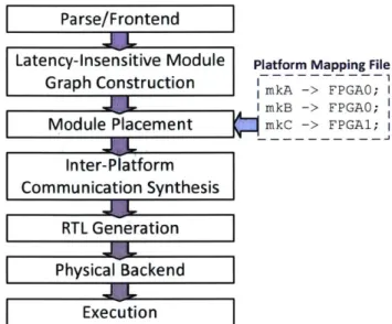
Platform Mapping File
mkA FPGAO; I I mkB -> FPGAO;
mkC -> FPGA1;
Figure 2-4: LEAP compilation flow.
2.1.3
LEAP Compilation
A typical LEAP program is composed of latency-insensitive modules, which communicate
with the rest of the system only by way of latency-insensitive channels. The goal of the
LEAP compiler [31] is to map the latency-insensitive modules onto an environment,
which may be a single FPGA or an aggregation of multiple connected FPGAs, and construct the physical implementation of the latency-insensitive channels connecting the mapped modules. During compilation, latency-insensitive modules are automatically connected through simple hardware FIFOs, if communicating modules are on the same platform, or through efficient, complex, inter-FPGA network, if communicating modules are on different FPGAs.
The LEAP compiler maps the target program onto a single or multiple FPGAs using the Bluespec compiler and FPGA-vendor tools as subroutines. The LEAP compilation flow is shown in Figure 2-4. First, the source code of the target program are passed to the Bluespec compiler. The LEAP compiler parses the intermediate files produced by the Bluespec compiler to construct a dataflow graph representation of the user program. Inside the graph, vertices correspond to latency-insensitive modules, while edges are the associated latency-insensitive channels. Then, the LEAP compiler maps the graph to the target execution environment consisting of single or multiple FPGA platforms based on a
Chapter 2. Background
platform mapping file, which specifies the associated platform for each latency-insensitive
module. The platform mapping file can be either provided by the programmer or
automat-ically generated by the LEAP compiler. After the latency-insensitive modules have been
placed, the LEAP compiler constructs the physical network connecting these modules
and produces a top-level Bluespec program for each FPGA platform. The generated
programs are passed to the Bluespec compiler for a second time to generate Verilog code
and then an FPGA-vendor tool chain to produce final physical implementations.
In this thesis, to optimize the network connecting LEAP memory clients on an
application-specific manner, we extend this LEAP compilation flow by adding a series of
compilation phases, which we refer to as the LEAP Memory Compiler (LMC). We will
describe LMC in full in Chapter 7.
2.2
Extending LEAP Memories to HLS Applications
To simplify implementation tasks while having tight control over architectural design
and optimizations, as mentioned in Section 2.1, LEAP uses Bluespec to assist its platform
service implementations. Bluespec SystemVerilog (BSV) [12] is a high-level hardware
description language (HDL) with syntax based on SystemVerilog and abstractions
in-spired by Haskell. Unlike C-based HLS programs, which are written in a sequential
computational model and thus have difficulty expressing irregular and complex parallelism
in memory hierarchies and on-chip networks, the behavior model of BSV programs is
fundamentally parallel. BSV programs are implemented based on a set of guarded rules,
which are called Guarded Atomic Actions and can be used to express complex concurrency
in hardware [70, 71]. This rule-based programming paradigm has a steep learning curve
but can generate efficient hardware with performance close to that of a hand-written,
RTL-based design.
While LEAP services are written in BSV, they can be used by applications written
in any synthesizable language, including RTL-based applications and kernels written in
C/C
++
and compiled through HLS. This means that designing FPGA programs can be
further simplified while maintaining high performance by integrating HLS applications
2.2. Extending LEAP Memories to HLS Applications
with a LEAP-generated platform. However, applications not written in BSV need to connect to LEAP services through shims, which may be a design burden for users without hardware experience. To improve LEAP usability for HLS programmers, we design wrappers that connect HLS kernels to LEAP memories through bus protocols and make some steps toward automating this integration process. Since HLS tools generally have limited support and optimizations for accessing external memories, integrating with optimized LEAP memories can provide a large performance benefit for HLS applications with high storage capacity demands.
The first set of HLS applications integrated into a LEAP-generated platform was done in collaboration with Felix Winterstein from Imperial College London and published in [95]. The HLS applications included in that paper as well as in this thesis were im-plemented by Felix and my contribution was to support the integration process. The HLS kernels are constructed using Xilinx Vivado HLS [94] (formerly AutoPilot [112] developed by AutoESL), which is one of state-of-the-art C-to-FPGA tools and has ex-tensive support for our evaluation boards. In Vivado HLS, directives can be used to guide compiler optimizations and to specify the I/O protocols for the application. Our HLS applications use Vivado's native bus protocol (the ap_bus protocol) to communicate with LEAP memories. The application kernels are first compiled to Verilog implemen-tations through HLS. Then we use a Verilog wrapper to embed the generated kernels into the LEAP platform using BSV's Verilog import feature. The wrapper acts as a bridge between HLS kernels and LEAP memories by converting bus-based transactions into latency-insensitive LEAP memory transactions.
To further improve the usability of LEAP memories, we also design wrappers to support HLS applications that use AMBA AXI4 (Advanced eXtensible Interface 4) protocol [6] to access external memories. In addition, we provide an automated flow to integrate applications that only uses a single LEAP private memory. Figure 2-5a shows an example of the automatically integrated system. The instantiated LEAP memory has multiple ports for applications with multiple kernels, each of which accesses the LEAP memory through a separate bus interface. The integration flow is shown in Figure 2-5b. First, the Verilog implementation of the target application core is generated through
Chapter 2. Background
LEAP Platform HLS Core Wrapper HLS Core Controller +.. rMemory Memory Memory
nterface Interface --- Interface
Adapter Adapter Adapter
N-Port LEAP Private Memory
(a) An example of integrated systems
Figure 2-5: Automating the integration of HLS applications
C/C++ Program HLS Core Generation Verilog HLS Wrapper Generation LEAP Compilation
Final FPGA Image
(b) Integration flow