ARC RATE PREDICTIONS AND
FLIGHT DATA ANALYSIS FOR THE SOLAR ARRAY MODULE PLASMA INTERACTIONS EXPERIMENT (SAMPIE)
by
Carmen Perez de la Cruz
S.B. Aeronautics and Astronautics
Massachusetts Institute of Technology, Cambridge, 1993
Submitted to the Department of
Aeronautics and Astronautics in Partial Fulfillment of the Requirements for the
Degree of
MASTER OF SCIENCE in Aeronautics and Astronautics
at the
Massachusetts Institute of Technology June 1995
@Massachusetts Institute of Technology 1995 All Rights Reserved
Signature of Author
Department of Aeronautics and Astronautics May 12, 1995 Certified by
Professor Daniel E. Hastings, Thesis Supervisor
Department of AeronauticsAnd Astronautics
Accepted by
Professor larold Y. Wachman, Chairman MASSACHUSETTS INSTITUTE
OrF -,rrt1.atnsy Department Graduate Committee
JUL
07
1995
LIBRARIES
ARC RATE PREDICTIONS AND
FLIGHT DATA ANALYSIS FOR THE SOLAR ARRAY MODULE PLASMA INTERACTIONS EXPERIMENT (SAMPIE) Submitted to the Department of Aeronautics and Astronautics
on June, 1995 in partial fulfillment of the requirements for the Degree of Master of Science in
Aeronautics and Astronautics
The increasing demand for high power systems may require that these systems operate at high voltages. The operation of solar cells at high negative voltages in the ionospheric plasma, however, may lead to arcing. Analytical and numerical models of the arcing process have been developed and show excellent agreement with previous experimental data. Using these models the arcing activity for the conventional cells in NASA's Solar Array Module Plasma Interactions Experiment (SAMPIE) and the Japanese Space Agency ISAS' High Voltage Solar Array (HVSA) experiment were predicted. Comparisons between the experimental and predicted arc rates for the SAMPIE experiment showed excellent agreement. Analysis of the SAMPIE flight data, along with the computer simulations, was conducted to examine the relationships between the arcing rate and the various solar cell properties, environmental variables, and solar cell parameters. No cell temperature dependence could be supported by the data, but a possible critical ion flux and critical neutral density is implied. The dependence of arc rate on voltage was fitted using a power law, an exponential form, and a form suggested by the analytical model. The last two fits showed an onset voltage supported by the data. The coefficients from these fits could not be interpreted physically, but they could be scaled with ion flux and electron work function to give accurate arc rates at the new conditions.
Acknowledgements
I must first thank my thesis advisor, Professor Hastings, who has always believed in me. Thanks for all the encouragement and support.
I'd also like to thank Dale Ferguson who patiently answered all my phone calls regarding the SAMPIE experiment.
Thanks to all my friends at the SSPL lab: Graeme, Derek, Guy, Jim, Mike, and Folusho who have made my past two years very enjoyable and entertaining. Karen, my partner in crime, I wish you the best of luck. I am especially thankful to Jim for all the white chocolates which made me smile countless times and for being always there for me. Mark, thanks for the sanity check.
Mom and Dad thanks for giving me the opportunity to pursue my dreams and for always being there for me. Nacho, thanks for being Nacho. Thanks to Cristina for all those chocolate hugs and kisses, and to David for giving me the solar cell kit so I could learn about solar cells.
Aoy thanks for being the best friend anyone could have. I'll miss you.
This work has been sponsored by NASA Lewis Research Center. I would like to thank Dale Ferguson and Barry Hillard for supplying me with the invaluable data from the SAMPIE experiment and Dr. Kuninaka and Dr. Cho for providing the information for the HVSA experiment.
Contents
Acknowledgements 5
1 Introduction 15
1.1 Background ... ... . ... 18
1.1.1 Space and Ground Experiments ... ... 18
1.1.2 Arcing Onset M odels ... 19
1.2 Recent Flight Experiments . . ... ... 23
1.3 Overview of This Research ... 24
2 Numerical and Semi-Analytical Models 25 2.1 Semi-Analytical Model for Conventional Cells . ... 25
2.1.1 EFEE Charging Time ... 26
2.1.2 Ion Charging Time ... 31
2.1.3 Total Charging Time ... 32
2.1.4 Breakdown Condition ... 32
2.2 Proposed Arcing Mechanism for WTC Cells . ... 37
3 Experiment Descriptions 41 3.1 SAMPIE Description ... ... 41
3.1.1 Diagnostic Instruments Description ... 42
3.1.2 Individual Experiments Description ... 42
3.1.3 SAMPIE Operations ... 47
3.2 HVSA Description ... ... 49
4 SAMPIE and HVSA Simulations 53 4.1 SAM PIE Simulations ... 53
4.1.1 SAMPIE Data Acquisition ... 53
4.1.2 SAM PIE Simulations ... 56
5 SAMPE Data Analysis
5.1 Arc Dependency on Various Parameters ... 5.1.1 Bias Voltage ...
5.1.2 Material Properties ... 5.1.3 Cell Geometry ...
5.1.4 Environmental Variables ... 5.2 Statistical Significance Discussion . ... 5.3 Data Analysis of Conventional Silicon Cells ... 5.4 Data Analysis of APSA Cells ...
5.5 Data Analysis of Metal Coupons . . . .
5.5.1 Dependency of Arc Rate in Cell Temperature ...
5.5.2 Dependency of Arc Rate on Neutral Density and Ion Flux 5.5.3 Dependency of Arc Rate on Bias Voltage ...
5.6 Data Analysis of Wrap-Through-Contact Cells ... 5.6.1 Arc Strengths ...
6 Conclusions
6.1 Suggestions for SAMPIE reflight ... A SAMPIE Experimental Data
65 . . . . . 65 . . . . . 65 . . . . . 66 . . . . . 67 . . . . . 67 . . . . . 68 . . . . . 71 . . . . . 71 . . . . . 72 . . . . . 73 . . . . . 73 . . . . . 78 . . . . . 92 . . . . . 96 101 . . . . . 104 105
List of Figures
1.1 Schematic of a Conventional Solar Cell ... .... 1.2 Schematic of a Wrap-Through-Contact Solar Cell ...
1.3 Model of the Conventional Solar Array Used for Numerical Simulations . 1.4 Arcing Sequence of a High Voltage Solar Array ...
2.1 Geometry for EFEE charging . ... 2.2 Typical Electric Field Run-Away . ... 2.3 Minimum Total Charging Time ...
2.4 Critical Ambient Neutral Density Variation with Temperature ... 2.5 PIX II Experimental Data and Numerical Results ...
2.6 Proposed Arcing Sequence of a Wrap-Through-Contact Cell ...
3.1 Hitchhiker-M bridge configured for OAST-2 mission ... . . 3.2 The SAMPIE Electronics Box and Sample Tray ...
3.3 The SAMPIE Experiment Plate ... .... 3.4 Metal Coupon Geometry ...
3.5 Deployment Configuration of the 2D array in the SFU ... .. 3.6 Characteristic Voltage-Current Curves . ...
3.7 Schematic of the Silicon Solar Cell with the Conductive Coating .... Bay-to-Ram and Bay-to-Deep-Space Orientations ...
Plasma Density measured by SAMPIE (corrected) in ram . ...
Electron Temperature measured by SAMPIE (corrected) in ram Experimental and Simulated Arc Rates for the Silicon and APSA Experimental and Simulated Arc Rates for the Gold Coupon . . Experimental and Simulated Arc Rates for the Copper Coupon . Experimental and Simulated Arc Rates for the Tungsten Coupon
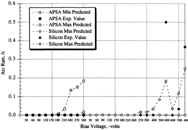
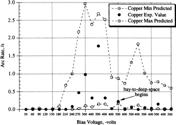
. . . . . . 54 . . . . . . 55 . . . . . . 55 cells . . . 59 . . . . . . 59 . . . . . . 60 . . . . . . 60
4.8 Experimental and Simulated Arc Rates for the Aluminum Coupon 4.9 Experimental and Simulated Arc Rates for the Silver Coupon. ..
4.1 4.2 4.3 4.4 4.5 4.6 4.7
4.10 Probability of an Arc Occurrence within a given Time ... . 64
5.1 Typical Ion Charging Time Curve and Voltage Threshold ... . 66
5.2 Intervals Yielding a 68% Confidence Level . ... 70
5.3 SAMPIE Arcing Data for the Silicon Cells . ... 71
5.4 SAMPIE Arcing Data for the APSA Cells ... ... . . . .. 72
5.5 Arc rate Dependence on Cell Temperature ... 74
5.6 Neutral Density and Ion Flux for SAMPIE Arcing Data ... . . 74
5.7 Arc rate Dependence on Neutral Density at -500 V . ... 76
5.8 Critical Ambient Neutral Density for Metal Coupons and Experimental Data 76 5.9 Arc rate Dependence on Ion Flux at -400V . ... 77
5.10 Arc rate Dependence on Ion Flux at -500V . ... 77
5.11 Arc rate at points of Constant Plasma Density ... . ... 78
5.12 Power fit to silver/aluminum data points at constant Plasma Density .... 79
5.13 Power fit to gold data points at constant Plasma Density ... .. 80
5.14 Arc rate experimental values for the different metal coupons ... . 81
5.15 Exponential fit to Ag/Al combination ... . . . . 81
5.16 Exponential fit to Ag/Al combination and scaled curves for gold and tungsten 83 5.17 MetalCoupons ... ... 83
5.18 Photograph of the Metal Samples after the Flight Experiment ... . 85
5.19 Exponential fit to Ag/Al oxide combination and scaled curves for gold ... 87
5.20 Exponential fit to Ag/Al combination and scaled curves for oxidized copper 88 5.21 Cho/Hastings simple fit to Ag/Al combination and scaled curve for gold .. 89
5.22 Cho/Hastings simple fit to Ag/Al combination and scaled curve for ion fluxes 89 5.23 Comparison of Ag/Al Experimental Data and Numerical Arc Rates 3=200 90 5.24 Comparison of Gold Experimental Data and Numerical Arc Rates ... 91
5.25 Comparison of Ag/Al Experimental Data and Numerical Arc Rates 3=300 91 5.26 SAMPIE Arcing Data for the WTC Cells . ... 93
5.27 Arcing Activity of Silicon and Space Station Cells ... 94
5.28 Normalized Arcing Activity of Silicon and Space Station Cells ... 94
5.29 Dependency of Arc Rate on Cell Area for WTC cells ... 95
5.30 Effect of Overhang in the Arcing Activity of WTC Cells ... 95
5.31 Peak Current in the Arcs Recorded by HVPS-1. ... 96
5.32 Power per unit area in Arcs in the Silicon Cells ... . . . . 97
5.33 Power per unit are in Arcs in Space Station Cells ... 98
5.35 Arc Populations in Space Station Cells at -650V . ... 99
List of Tables
3.1 SAMPIE Low Voltage Biasing Sequence ... 48
3.2 SAMPIE High Voltage Biasing Dwell Times . ... 48
3.3 Extracts from the Timeline of the SAMPIE Experiment . ... 48
3.4 Timeline for HVSA Experiment ... 51
4.1 SAM PIE Cell Data ... 57
4.2 Work Functions of the Metal Samples and Oxides ... 57
4.3 Environmental Parameters for Minimum/Maximum Arcing ... 58
4.4 Environmental Parameters for Minimum/Maximum Arcing for SFU orbit . 62 4.5 Silicon Cell Data ... 63
List of Symbols
A Fowler Nordheim coefficient (1.54 x 10-6 x 104.52Ow/ /Ow AV 2)
B Fowler Nordheim coefficient (6.53 x 10W9!i V/m)
Cdiele capacitance of dielectric (F/m2)
Cfront capacitance of coverglass front surface (F)
d thickness of dielectric (m)
di thickness of coverglass (m)
d2 thickness of adhesive (m)
dgap gap distance between cathode and anode (m)
di distance of electron first impact point from triple junction (m)
do overhang distance of coverglass (m)
do critical overhang distance of coverglass (m)
Ee electric field at emission site (V/m)
E electron incident energy on dielectric plate (eV)
E,,a electron incident energy for maximum secondary electron yield (eV)
ETJ electric field at triple junction (V/m)
E, electric field of coverglass (V/m)
E2 electric field of adhesive (V/m)
jec electron current density from conductor (A/m2)
je secondary electron current density from dielectric (A/m2
)
jFN Fowler-Nordheim current density from the conductor (A/m2)
jid ion ram current density to the dielectric (A/m 2)
ne plasma number density (m- 3)
nes emission site number density (m- 2)
me electron mass (kg)
mi ion mass (kg)
R arc rate (sec-1)
rs sheath radius (m)
Sreal emission site area determined by accounting for electron space charge
effects (m2)
Te electron temperature (eV)
Ti ion temperature (eV)
Vrc voltage at which last arc occurred V
Vbias bias voltage of interconnector/conductor V
Ve voltage which minimizes arcing time V 14 initial voltage before solar cell charging V
v~oo mean speed of ions entering sheath (m/sec)
vX electron velocity in the x direction (m/sec) vy electron velocity in the y direction (m/sec)
y distance of emission site from the triple junction (m)
P field enhancement factor
AQ charge lost from one coverglass by one discharge (C)
Ed, relative dielectric constant of coverglass
Ed2 relative dielectric constant of adhesive
S1 energy at yee = 1 (eV) Oc potential of conductor (V)
qi potential of coverglass-adhesive interface (V) W work function (eV)
yee secondary electron yield
7,max maximum secondary electron yield at normal incidence
77 factor accounting for difference in electric field at emission site and triple junction
i incident impact angle of electron onto the dielectric surface
a surface charge density (C/m2)
Tarc time between arcs (sec)
Tefee EFEE charging time (sec)
Tim ion charging time (sec)
Tex, experiment time (sec)
S factor accounting for difference of dielectric constants between coverglass and adhesive
Chapter 1
Introduction
The power system chosen for a space mission depends upon the mission duration and objectives. For short time and low energy requirements, the best power systems are electro-chemical systems such as fuel cells, but for missions with power requirements in the range of 0.1 W to 100 kW, photovoltaic power is the most commonly used power system. Cur-rently, most of these systems operate at low voltage levels, typically 28 V. Future missions may require these systems to be operated at higher power levels, in the range of 10 kW to 1 MW. To meet these requirements the systems may be operated at high voltage levels or high current levels. Operation at high voltage levels is preferred for two reasons. The first is that the resistive loss during power transmission for a given power system is lower when the power system operates at high voltages rather than high currents. The second reason is that the mass of the distribution cables will be reduced by distributing the power at high voltages rather than high currents. Thus, power distribution at high voltage levels is desired. In this research, the term high voltage is used to refer to voltages with an absolute value higher than 100 V. Proposed systems range from -160 V for the International Space Station Alpha to thousands of volts for orbital transfer vehicles using solar electric propulsion.
A schematic of a conventional solar cell is shown in Fig. 1.1. The coverglass protects the semiconductor (the solar cell) from the radiation environment. Adhesive is used to bond the coverglass, semiconductor, and substrate. Metal interconnectors allow the current to flow between adjacent cells. The required voltage is attained by connecting the cells in series and the required power level is attained by placing these strings of cells in parallel.
As seen in Fig. 1.1, conventional solar cells will have some part of the metallic intercon-nector exposed to the environment. This design choice allows the arrays to be flexible and to thermally expand or contract when entering or leaving eclipse. The metallic interconnector, along with other surfaces of the spacecraft which allow the passage of current, will collect current from the space plasma. The charge accumulated by the spacecraft must satisfy
solar cell
substrate
interconnector
(contact)
Figure 1.1: Schematic of a Conventional Solar Cell
8p 0
+ - = 0, (1.1)
derived from Gauss' law and Ampere's law. In steady state, the net current collected by the spacecraft is zero. Hence, to satisfy this condition, some of the surfaces in the spacecraft will be negatively biased and collect ions and the rest will be positively biased and collect electrons. Because the mass of an electron is much smaller than the mass of an ion, the electron current collected by a positively biased surface will be much larger than the ion current collected by the same surface if negatively biased at a comparable voltage. Thus, to satisfy the zero net current condition, most of the surfaces of the spacecraft, including the solar arrays, will float negatively with respect to the plasma. For example, major parts of the Space Station are expected to float at approximately -130 V relative to the plasma [3], which is close to the maximum operational voltage, -160 V.
High voltage solar arrays have been found to interact with the ambient plasma in several detrimental ways, resulting in operational inefficiencies. When positively biased, arrays can collect an anomalously large current, a phenomenon known as "snapover". For large voltages this may lead to a significant leakage power loss [42]. When the cells are operated at large negative voltages, arc discharges may occur. An arc is defined as a sudden current pulse up to an order of an ampere lasting a few microseconds or less. It is often accompanied
solar cellw substrate
interconnecto (contact)
Figure 1.2: Schematic of a Wrap-Through-Contact Solar Cell
by a flash of light at the edge of the coverglass. These arc discharges may give rise to electromagnetic interference (EMI), enhance the local plasma density, and cause damage to the solar cell. Lastly, high accelerated ions will collide with the arrays and give rise to enhanced drag on the spacecraft [14].
To eliminate the interaction between the conducting surfaces and the ambient plasma, these surfaces may be covered with an insulator. This is the principle behind the design of a new type of solar cell, the wrap-through-contact (WTC) solar cell, developed by NASA for the Space Station [44]. A schematic of this type of cell is shown in Fig. 1.2. The interconnectors of these cells are no longer exposed to the plasma but instead pass underneath the substrate and connect to the middle of adjacent cells under the coverglasses. However, in this new design, the semiconductor is still exposed to space along the edge of the cell. Even if all conducting surfaces were to be covered, the problem is not permanently solved. While in orbit, cracks may develop due to severe thermal cycles or particulates striking the insulating surfaces and again leave some parts of the interconnector or semiconductor exposed.
1.1 Background
1.1.1 Space and Ground Experiments
Arcing on high voltage solar arrays has been observed in both ground and space experiments. The first observation of arcing on solar cells in a plasma chamber was made by Herron et
al. [18] in 1971. The solar cells were biased between +16 kV and arcing was observed at bias voltages as low as -6 kV with a plasma density of 108 m- 3. The occurrence of arcs in space was verified by the first Plasma Interactive Experiment (PIX I) [12] in 1978. PIX I, flown as an auxiliary payload on Landsat 3's Delta rocket, obtained data for a period of four hours in a 920 km polar orbit. During this period, a solar array consisting of twenty four 2cmx2cm conventional silicon solar cells were biased to +1000 V. Arcing was observed at voltages greater than -750 V.
A more extensive experiment was conducted by PIX II in 1983. A more sophisticated version of PIX I, PIX II was also flown as an auxiliary payload on a Delta launch vehicle into a 900km polar orbit. In this experiment the solar array consisted of five hundred conventional silicon cells again biased to 1000V. Arcing was observed at voltages as low as -255V. A few problems were encountered when interpreting the flight data. Unexpected tumbling of the spacecraft placed the Langmuir probe in the spacecraft wake, making the Langmuir probe readings unreliable. Furthermore, if an arc occurred at high voltages, the power supply was often shut down for the rest of the data taking cycle. The data from the PIX II flight and ground tests was studied by Ferguson [7], who concluded that the arc rate R was directly proportional to the plasma density. Ferguson obtained the following relationship where the arc rate varies with bias voltage in a power law fashion given by
S= 1.4 x 10⁻¹⁰ (-V)3.0 9 3 103) (1.2)
for the flight data, and
R = 1.82 x 10- 8 (-V)5. 5 1 (1.3)
in ground tests at high density, with a mean plasma density of 1.5 x 104 cm- 3, where V is the bias voltage and n is the plasma density in cubic centimeters.
Other ground experiments offer some insight on the characteristics of the arcing phe-nomenon. Experiments conducted by Miller [30], Kuninaka [25], and Fujii et al. [11] confirm that the presence of a dielectric material near a biased conductor is essential for arcing to occur. Fujii et al. [11] tested three metallic samples under the same plasma
con-ditions. The two samples that were covered with 200 plm thick fused silica, simulating a coverglass, arced at voltages as low as -450 V. The third sample without a coverglass did not show arcing until -1000 V when the arcing occurred at the substrate. In the wrap-through-contact cells, where the conductive surfaces have been shielded from the plasma, the arcing threshold observed in ground experiments ranged from -210 V to -457 V with respect to the plasma potential [33].
In an experiment conducted by Snyder [37], the potential just over the coverglass surface was measured. Before an arc occurred the potential was near the plasma potential, but when an arc occurred the potential dropped significantly, on the order of a hundred volts. In a different experiment, Snyder et al. [38] observed current emission after the plasma source was no longer in operation. Inouye and Chaky [22] observed that the current emitted from the solar array sample during arcing was greater that the value expected from photoemission. Several experimental observations have led to qualitative relationships between the arcing rate and different parameters. Many experiments have shown that the arcing rate decreases as the experiment continues, suggesting that the surface conditioning affects the arcing rate. Kuninaka [24] varied the temperature of the array from 1000C to 5000C and observed that
the arc rate decreased as the temperature increased. Leung [27] observed that the wrap-through-contact cells arced less than the conventional cells. Upschulte et al. [45] observed that overhanging the coverglass over the adhesive by 10,20Am, somewhat shielding the interconnector, suppressed the arcing activity considerably.
1.1.2 Arcing Onset Models
There are two different types of theoretical models which offer an explanation of the arcing onset mechanism. The first, proposed by Parks et al. [34] based on the previous work of Jongeward et al. [23], attributes the arcing onset to the Malter [29] effect at a thin dielectric layer on the conductor surface. The second, proposed by Cho and Hastings [4] based on previous work of Hastings et al. [16], attributes the arcing onset to a discharge in the neutral gases desorbed from the dielectric surface.
The arcing mechanism proposed by Parks et al. [34] is described by the following se-quence:
(1) A dielectric impurity layer is formed on the conductor surface.
(2) Ions attracted to the negatively biased conductor are accumulated on the dielectric layer and enhance the electric field in the layer.
the dielectric.
(4) The emitted electrons have ionization collisions while being accelerated within the dielectric, leaving positive charges behind as they are emitted from the dielectric-vacuum interface.
(5) The remaining positive charge further enhances the electric field within the dielectric layer.
(6) The resulting rate of change of the electric field in the insulating layer is given by a combination of Gauss' Law and Ampere's Law,
d
E-- (Er E-d - Ed-) = ji + iJ-dedd Pa- - jm-d, (1.4)
where Er is the dielectric constant of the insulating layer, Em-d is the electric field in the dielectric layer, Ed-v is the ambient electric field at the dielectric-vacuum interface, ji
is the ion current density, ad is the ionization rate per unit distance inside the layer, dd is
the dielectric layer thickness, Pd-, is the probability that the electrons are emitted from the dielectric-vacuum interface, and jm-d is the Fowler-Nordheim emission current at the metal-dielectric interface which is given by
im-d = AE_ae- , (1.5)
where A and B are the Fowler-Nordheim emission coefficients are given by
1.54 x 10-6104.52/ (A/ (1.6)
A =1 (A/V2), (1.6)
B = 6.53 x 10⁹ 5s(V/m), (1.7)
where $, is the work function of the metal in eV. If the factor ea
ddd Pd_, is greater than unity, a positive feedback mechanism is created at the metal-dielectric interface, leading to a runaway of the field and the emission current by increasing Em-_dmonotonically in time.
The arcing onset mechanism proposed by Cho and Hastings [4] modeled the geometry of a conventional cell as shown in Fig. 1.3. The dielectric consists of the coverglass and the adhesive. The conductor is the interconnector between the cells which connects the adhesive-solar cell interface to the substrate-solar cell interface of the adjacent cell. Since the voltage drop across the actual solar cell is much lower than that across the dielectric, the solar cell has not been included in the model. Through the use of computer particle simulations, the above system was used to study the arc initiation process at the triple
Triple Junction
Front Surfac M
VKCD
-Intercornuector
Figure 1.3: Model of the Conventional Solar Array Used for Numerical Simulations
junction, the point where the dielectric, conductor and plasma meet. The arcing onset mechanism that resulted form the numerical simulations is illustrated in Fig. 1.4 and is described by the following sequence:
(1) Ambient ions, attracted by the negatively biased conductor, charge the dielectric front surface (parallel to the conductor), but leave the side surface effectively uncharged. (2) As the potential of the front surface approaches zero, a strong electric field, given by E=V/d (where V is the bias voltage and d the dielectric thickness), is set up between the triple junction and the front surface.
(3) This strong electric field, aided by field enhancement at sites in the conductor surface, induces a pre-breakdown enhanced field electron emission (EFEE) current showing the characteristic of the Fowler-Nordheim emission current shown in Eqn. 1.5. In addition, electrons are also released due to the bombardment of the conductor surface by the ambient ions.
(4) Some of the emitted electrons strike the side surface of the dielectric causing the release of secondary electrons and the electron stimulated desorption of neutrals adsorbed on the dielectric surface. If the secondary electron yield is greater than unity and the electrons have an escape path, the side surface charges up positively, providing a positive feedback mechanism to further enhance the electric field at the conductor surface.
(5) As the electric field increases, the electron emission current increases until it is limited by the negative space charge of the emitted electrons.
(6) Once the neutral density becomes high enough, ionization begins due to collisions between electrons and neutrals.
(7) If the neutral density is very high, Townsend breakdown occurs as proposed by Hastings et al. [16]. Even if the density is not high enough for Townsend breakdown to
= -V interconnector secondary electron multiplication
C+
(+)
(+)
I
charging
of
front
surface
charging
of side
surface
*= -V
enhanced field emissiondischarge
recharging
by ions
S=-V
Figure 1.4: Arcing Sequence of a High Voltage Solar Array
occur, breakdown is still possible if the positive ion space charge can cancel the negative electron space charge and enhance the field at the conductor.
(8) The arcing time is the minimum of the sum of the ion and EFEE charging times for all the emission sites on the conductor.
(9) A discharge wave created by the arc resets the charging process at all of the emission sites within the area covered by the wave.
Cho [4] suggested several possible mitigation strategies. Among them was to hide the triple junction from the plasma by causing the coverglass to overhang over the adhesive
and solar cell. Numerical simulations conducted by Cho [4] and Mong [31] showed that the EFEE charging time increased dramatically, resulting in a decrease in the arcing rate. The numerical results showed that the first impact point of the electrons emitted from the conductor will be in the back surface of the coverglass. The secondary electrons emitted from the back surface cannot escape because the coverglass is blocking their trajectories. The accumulation of these electrons will decrease the potential of the back surface and consequently lower the electric field at the triple junction. When electrons begin to hit the adhesive, they release secondary electrons which leave the side surface positively charged. The electric field at the triple junction then begins to increase. However, this increase in the electric field at the triple junction was found to occur at a much later time compared to the one for the conventional geometry. Mong [31] derived an expression for the critical overhang distance, such that overhangs greater than this length will decrease the arcing activity dramatically.
1.2 Recent Flight Experiments
Three recent flight experiments have been designed to study the interaction of high volt-age solar arrays with the plasma environment. In these experiments, different solar cells, space materials, and arc mitigation strategies were tested. The Solar Array Module Plasma Interactions Experiment, SAMPIE, was developed by the National Aeronautics and Space Administration (NASA). SAMPIE was among the experiments flown in the payload bay of the Space Shuttle Columbia in March, 1994. The shuttle placed itself in a circular orbit at a 390 inclination and a 300 km altitude. The Photovoltaic Array Space Power Plus Diag-nostics (PASP Plus) experiment, is the primary experiment on the Advanced Photovoltaic and Electronics Experiments (APEX) satellite. This satellite is part of the Space Test Pro-gram (STP) of the Air Force's Space and Missiles Center. Launched in August, 1994, this experiment will operate from one to three years. The satellite was placed in a 355 x 2544 km orbit at a 700 inclination, thus allowing the solar cells to be exposed to a large range of the space plasma, neutral, and radiation environments. Lastly, the High Voltage Solar Array (HVSA) experiment, developed by the Institute of Space and Astronautical Sciences (ISAS) is integrated as one of the eleven experiments conducted on the first flight of the Space Flyer Unit (SFU). SFU was launched in the Japanese H-II rocket on March, 1995, injected into a 486 km altitude and 28.50 inclination orbit, and retrieved by the Space Shuttle
1.3 Overview of This Research
In the future, solar arrays may be chosen to satisfy high power requirements. To save mass and reduce the resistive losses, the solar arrays may be operated at high voltages rather than high currents. Yet, when solar arrays are biased to high negative voltages, the current collecting surfaces interact with the plasma environment, leading to operational inefficiencies. The occurrence of arcs will degrade the solar array performance and produce electromagnetic interference which may affect nearby instruments. Cho and Hastings [4, 15] developed a semi-analytical model based on the numerical and theoretical work to predict the arcing rates for a solar array given the environmental parameters. This model has predicted arc rates that showed a good agreement with the data for ground experiments and PIX II
flight data.
The objectives of this research are the following
1. To use the semi-analytical model to predict the arc rates for the SAMPIE and HVSA flight experiments and assess its agreement with the experimental data.
2. To determine the correlations between arcing rate and the various material properties, environmental variables and experimental parameters as suggested by the model by using the flight data from the SAMPIE experiment.
In Chapter 2, the semi-analytical model for the conventional geometry cells developed by Cho and Hastings is reviewed and a possible mechanism through which WTC cells arc is presented. In Chapter 3, the SAMPIE and HVSA experiments are described. The are rates predicted for these experiments, obtained using the semi-analytical model, are shown in Chapter 4. In Chapter 5, the flight data obtained from the SAMPIE experiment is analyzed. Finally, conclusions are made about the arcing behavior of the different cells and the validity
Chapter 2
Numerical and Semi-Analytical Models
Cho and Hastings developed a semi-analytical code based on the numerical simulation of their proposed arcing onset mechanism for conventional geometry cells, shown in Fig. 1.4. The code predicts the arcing activity for a given solar array using parameters chosen from probability distribution functions obtained from numerical simulations using a particle-in-cell (PIC) code. The semi-analytical code was then modified by Soldi and Hastings [39] to model the physics more accurately and to include experimental limitations. This chapter will review the semi-analytical formulas in the current code and describe a proposed arcing mechanism for the WTC cells.
2.1
Semi-Analytical Model for Conventional Cells
When an arc occurs, some of the stored charges on the coverglass are lost. Experimentally it has been observed that during the arc discharge, the potential of the coverglass drops by a few hundred volts from its steady state value of about +5 volts [37]. Since the electric field at the triple junction also drops during the arc discharge, the field emission ceases to charge the coverglass and the lost charge will be restored through ambient ions. When sufficient charge is restored, the electric field becomes high enough to restart the enhanced electron
field emission (EFEE) charging of the dielectric until the next discharge occurs.
The numerical results have shown that the critical condition for arcing onset after EFEE charging has been initiated is whether the desorbed neutral density is larger than the critical value of approximately 6 x 10²¹ m-3 [4]. If the neutral density is above this value, a break-down occurs and this mechanism is labeled as a "big arc." Big arcs are typically seen as current pulses on the order of amps. The surface discharge wave created from the breakdown will expand radially away from the arc spot. Assuming that the wave front is expanding semispherically, the expansion speed of the wave front vd is inversely proportional to the area covered by the wave. Therefore, vd = co/rdiS2where rdi is the radius of the wavefront.
From a fit to experimental measurements, the co coefficient was found to be 6.0 [4]. Thus, assuming a maximum arc duration of 10 Ils the discharge wave can cover an area of 0.01 m2. The charging processes in the sites within the discharge wave area, also known as the area of correlation, will be reset.
If the density is below the critical value, the electron current just becomes space charge limited and will eventually relax without leading to a breakdown. In this case, a very short current pulse would be seen, without an arc flash or arc damage. This current pulse, referred to as a "small arc", will not create a discharge wave. Thus the charging processes within the correlated area will not be affected until another "big arc" occurs. Results from numerical simulations showed that the current seen from a small arc is on the order of microamps to a few milliamps. For experiments such as SAMPIE and HVSA, the minimum current levels detectable by equipment are 20 mA and 300 mA respectively. Consequently, only the occurrence of big arcs would be recorded by these experiments.
In the simulations, the total area of the array is divided into correlated areas and the arcing rates in each correlated area are calculated independently of each other. The arc rates in each correlated area are then summed to obtain the total arc rate for the solar array. The arcing rate is obtained by dividing the number of arcs with currents above the threshold by the experiment time.
From the above discussion, the time between big arcs, 1-ar,, is the minimum charging time
of all the sites on the conductor within a correlated area which satisfy the critical condition for arcing onset and is given by
Tarc = min(Tion + 7Tefee), (2.1)
where o,,n is the time during which the ions restore the lost charge in the dielectric and Tefee is the enhanced field electron emission charging time. In this section the semi-analytical formulas for the EFEE charging time, ion charging time, total charging time, and the breakdown condition will be reviewed. A detailed derivation of these formulas can be found in Ref. [4].
2.1.1 EFEE Charging Time
The geometry considered for EFEE charging is shown in Fig. 2.1. The dielectric surface is charged by j,c(y), the electron emission current emitted from location y on the conductor and j,(x), the secondary electron current density emitted from location x. The rate of change of the surface charge density on the dielectric surface is given by
conductor triple juction d2 d :adhesive front coverglass surface
Figure 2.1: Geometry for EFEE charging
d(x, t) = - P(x,y, t)jec(y, t)dy - P(x, x', t)jee(x', t)dx' + jee(x, t) (2.2)
where P(x, y, t) is the probability that an electron emitted from location y to y + dy on the conductor will hit the dielectric surface in the range x to x + dx and P(x, x', t) is the probability that an electron emitted from location x' will hit at location x. The secondary electron current at each location x is given by
jee(x, t) = ee(x, y)P(x, y, t)jec(y, t)dy + ee(x, x')P(x, x', t)jee(x', t)dx' (2.3) where yee(x, y) is the secondary electron yield at location x due to the electrons emitted
from the point y. The rate of change of the surface charge density at the first impact point, x = di, is calculated by integrating Eqn. 2.2 neglecting the contribution of secondary
electrons which yields
d - (ee - 1)jec
(2.4)
t = di
where Sr,,a is the area of the emission site at the dielectric vacuum interface. The electric field at the triple junction, x = 0, can be expressed as
ETJ =
=
d (2.5)where qd is the potential between the first impact point and the triple junction, Ciiele is the capacitance of the front surface and the factor ( is introduced to account for the discontinuity of the electric field due to the difference in the dielectric constants of the adhesive and coverglass. If the first impact point of the emitted electrons on the dielectric surface is within the adhesive, di < d2, then ( is unity. If the impact point is within the
coverglass, then ( is given by
d2 -d2)1 (2.6)
The electric field at an emission site in the conductor, Ee, will differ from the value at the triple junction, ETJ. The numerical simulations revealed that the difference was only a function of the distance from the site to the triple junction and the factor '7 was introduced
to account for this difference. Thus, the electric field at the emission site is given by
Ee = rET = rCd d (2.7)
Cdieledi
Substituting Eqn. 2.7 into Eqn. 2.4 results in
dEe Cd ed 3jec (2.8)
The current emitted from an emission site in the conductor surface is described by
jec = A SY Z E'exp(- ), (2.9)
the Fowler-Nordheim expression for field emission due to dielectric inclusions on the conductor's surface. The factor SFN/Sreal has been introduced to account for the negative space charge effect near the emission site. Srea, is the emission site area on the conductor surface and SFN is chosen to obtain the same current observed in experiments. A and
B are the Fowler-Nordheim coefficients given by Eqns. 1.6 and 1.7. The term
i
is theelectric field enhancement factor assigned to the emission site and has been introduced to adjust for the observation of experimental emission currents at applied fields typically 100 to 1000 times smaller than those predicted by the Fowler-Nordheim expression. The field enhancement is attributed to manufacturing defects or impurities on the interconnector surface. Microprotusions on the surface can lead to an enhancement factor in the order of a hundred while a dielectric layer formed on the metal surface can yield enhancement factors in the order of a thousand. The value of / is not measured since it is a costly and difficult process. Therefore, in order to model the variation of the conductor surface, the semi-analytical code assumes a distribution of f values. The 3 value for an emission site is
chosen randomly from a distribution of values between I and 2000, with an average value of 200.
The resulting rate of change of the electric field at an emission site on the conductor, E, is given by
dEe d- (ee-1)V A SFN2E B (
N 02E exp . (2.10)
dt Cdieled? SreaE
The values of r, di, and Cdiele are functions only of y. The following formulas were calculated from polynomial fits of the numerical results. r is given by
n=4
77 = 1 + a,((y - 1)2n - 1), (2.11)
n=l
where y = y/(dgap/2), y is the distance from the emission site to the triple junction, and
dga, is the interconnector length. o is the value of ( with di = d, + d2.The first impact point,
di is given by
d =d n=4b, d
(2.12)
R= 1
where d = dl + d2. The capacitance per unit area of the dielectric side surface, Cdiele(di) is determined from a fifth order polynomial fit to the results of a capacitance matrix scheme
[21]. In such scheme the change in the surface potential 6,, 3 due to a unit charge Oa placed at a gridpoint on the dielectric is calculated by solving the Poisson equation, V2&6 s,j = 6i,j.
Repeating this process for all the gridpoints on the dielectric, yields a matrix relating the potential at a gridpoint on the dielectric surface and the charge density at any other point on the dielectric surface. Inverting this matrix, a matrix of capacitances is obtained and the coefficients cn result from a fifth order polynomial fit to the diagonal entries of this matrix.
Cdiele (di) 1
Chrm :n=e n (2.13)
where C,,om is the capacitance per unit area of the front surface
1
Cnorm = d, 1 (2.14)
Ed, Ed2
The value of ,,ee, the secondary electron yield, is also a function of y and is given by Ref. [13] as
Ee0
t
efee
Figure 2.2: Typical Electric Field Run-Away
where 7, is the maximum secondary electron yield at normal incidence and Em, is the electron incident energy for the maximum secondary electron yield. Ej is the incident energy of the emitted electrons impacting the dielectric surfaces and is given by
ETJdi JO
d-Ej=ed = E d- V (2.16)
Sd
and Oj, the incident angle of those electrons at the first impact site, is given by
Oi = arctan . (2.17)
If the secondary electron yield ,ee is assumed to be constant, Eqn. 2.10 can be integrated, yielding an electric field Ee(t) with the characteristic shape shown in Fig. 2.2 and given by
Ee(t) = Eo (2.18)
1 + ln (1-exp(- B)( )C
where C is the constant given by
(7ee - 1)> A SFN/2
C = rlC A )3 (2.19)
Cdieledi Sreal
and E,,o is the initial electric field at the electron emission site on the interconnector. The theoretical run-away time for a constant secondary electron yield, t = Tefee, is derived by setting the denominator in Eqn. 2.18 to zero. Thus, the field emission electron charging time -fe is given by
1- exp(- B)
exp(- BE
)o
)3 B
eexp--- = -- B C (2.20)
Cdiele rA S exp ( B (2.22)
(yee -1) vreaiqcA FNBO \EI
The initial electric field at the emission site Eo can be expressed in terms of the potential difference between the coverglass front surface and the triple junction as
V
Eeo = 7d o. (2.23)
Thus, Tef,, is given by
Cdieled? (3Bd
Tefee(V) = (-e_ 1)Aed exp
(
. (2.24)The implicit assumption in this analysis is that the secondary electron yield is greater than unity. If the yield is less than unity, positive charging of the dielectric side surface will not occur and the field will not run away. Cho also showed that even when taking into to account the angle of incidence, the incident energy which gives Yee = 1 will be about twenty electron volts. Therefore, as long as the voltages considered are in the order of a hundred volts, the secondary electron yield will remain above one.
Hence, the parameters that affect the EFEE charging time are the secondary electron yield, the capacitance of the side surface, the constants associated with the Fowler-Nordheim current, the parameters of the emission site, the first impact point on the dielectric "surfaces, and the bias voltage. The coefficients A and B are only determined by the surface work function, , and as noted above di, 7, (, and Cdiele are only functions of y. For a given geometry, the independent parameters which affect the EFEE charging time are only y,
Srea, SEN, ,, and V,. In the numerical code, Yee is not assumed to be constant and therefore
Tefee must be calculated numerically from Eqn. 2.10. However, in the data analysis Yee is assumed to be constant and rfe,, is given by Eqn. 2.24.
2.1.2 Ion Charging Time
The ion charging time is the time during which the ambient ions restore the lost charge of the front surface after an arc has occurred. If an arc occurs when the potential difference between the front surface and conductor is Va and the coverglass front surface loses charge
AQ, then the potential difference drops to V - AQ/Cfr,,t, where Cfrt is the capacitance
of the front surface given by
1
The ambient ion charging time for the voltage to recover to the value V, is then given by
Tio, = front (2.26)
enevioAcell
where vion is the mean speed of the ions entering the sheath and enevio is the ion flux to the coverglass front surface of area A, 1u. For ground experiments vio is given by c/4 where S= ,. For flight experiments it is given by the component of the orbital velocity onto the dielectric front surface, vio = vobit sin a where a is the angle of attack of the arrays to the ram direction (at angle of attack of 900 the spacecraft velocity vector and the vector normal to the solar cell's front surface are parallel).
2.1.3 Total Charging Time
When an arc occurs, the coverglass is recharged by ions and the electric field at the triple junction increases. The EFEE process may start whenever the surface of the conductor feels a strong enough electric field. The total charging time for each emission site is determined numerically by finding the value of V, that minimizes 7chr = To,, + Tefee. The total charging time as a function of V for a constant secondary electron yield is shown in Fig. 2.3 where
ro(Ve) is the premultiplier in Eqn. 2.24. Substituting the EFEE and ion charging time
equations in Eqn. 2.1 the following expression for the time between arcs is obtained
(Ve - (Varc - ))Cfront Cdieled? Bd )
c g = + ( - exp (2.27)
enevionAceaI (7ee - 1) q BS V
This expression assumes that the time during which the neutrals are ionized is short and therefore it can be neglected.
2.1.4 Breakdown Condition
Once the electric field has run away, the breakdown criterion must be judged. Flashes of light observed in experiments on high voltage solar array arcing indicate that arcing is a fairly localized phenomenon, confined near the interconnector and the coverglass. Therefore the breakdown occurs in a length scale less than a millimeter. The product of the outgassed neutral density and this length scale, d, gives values which fall in the semi-vacuum region between the Townsend breakdown region, where the ionization mean free path Am,fp is smaller than the path length d, and the vacuum breakdown region where
/chrg tion+tefee
E
-AQ
E
(Ve-(Va-
Q ))Cront
Cfr
STion- fnt,
lenoVionAcen tefee=o(Ve)-OXP(Bd
P
I
P1oVe
v
Ve
EFEE charging begins when the voltage between the
triple junction and the cover-glass front surface recovers to this value.
mechanism of gas breakdown in this intermediate region. From this theory and numerical results, a critical neutral density, n,c, above which the positive ion space charge balances the increase of negative space charge, was determined to be approximately 6x 10²¹ m-3 Therefore breakdown occurs at a site if the desorbed neutral density n, at the site is greater than the critical neutral density n,e. The desorbed neutral density at each emission site is given by [4] by
n, = 2.08 2e (2.28)
e e me Eseid
where N, is the adsorbed neutral density on the dielectric surface before the intensive outgassing due to the EFEE begins, QESD is the electron stimulated desorption cross section, co is the dielectric constant of vacuum, e is the electron charge, me is the electron mass, Ese is the secondary electron energy in eV, E,,s is the energy for a secondary electron yield of unity, d is the dielectric thickness, d = di + d2, and e is the average speed of the desorbed neutrals. These neutrals are assumed to be at the temperature of the dielectric surface T,, so that
= 8s (2.29)
V irm
where m, is the mass of the neutrals (assumed to be water). The rate of change in the adsorbed neutral density N, is calculated by the difference between the thermal stimulated desorption of neutrals and the flux of ambient neutrals onto the dielectric surface. N, can be calculated by solving the following equation
dt = n+ 1 - ' - N, exp (2.30)
dt 4 Nno NTs
where k? is the neutral thermal desorption coefficient, ED is the adsorption energy, n,, is the ambient neutral density, and No is the neutral surface density for monolayer coverage
of the surface. The term 1 - Ns/NNo is an approximation for the probability that a neutral
striking the surface will stick and L, is the component of the neutral flux to the side surface
due to the orbital velocity given by
Fn = nnaVorbit cos a, (2.31)
with vobit being the orbital velocity and a the angle of attack of the arrays to the ram. The surface neutral density, as a function of time, is therefore given by
where C, and C2 are given by
C1 = Fn + nna- (2.33)
4
C2 - + k exp ED (2.34)
Nno 1 (- T,)
Substituting Eqn. 2.32 in Eqn. 2.28 the steady state critical ambient neutral density, nnac, required for arcing onset can be derived and is given by
k' exp( E)
n,ac C (2.08 = 0 12 VeE - )(c/4 + Vorbit Cosa) (2.35)
flflcC e M, Eaeid2 e Nno
This density is a function of the cell temperature, voltage, electron stimulated desorbtion cross section QESD, angle of attack, dielectric thickness and the secondary emission proper-ties of the dielectric. Thus, for a given cell, voltage and value of QESD and orientation, the critical ambient density required for breakdown can be determined for various cell temper-atures. For example, the maximum steady state critical ambient neutral density needed for breakdown at typical bias voltages used in the SAMPIE experiment for silicon cells in the
ram orientation is shown Fig. 2.4. The value of QESD chosen for the curves, 10-19 m2, was
chosen to agree with the value of ESD yield, NQESD, recorded in numerous measurements [6]. As seen in Fig. 2.4, the ambient neutral density needed to allow breakdown is a strong function of the cell temperature. The curves indicate that for a given cell temperature there is a critical ambient neutral density above which breakdown will occur. Similarly, for a given ambient neutral density, there exists a cell temperature above which no arcing will occur.
Using the semi-analytical model, the arcing rates may be calculated for conventional geometry cells. To calculate arc rates, the solar array area is divided into a finite number of correlated areas. For each emission site in the conductor, parameters are chosen randomly from distribution functions. The enhancement factor 3 is chosen assuming a distribution
function f(f3) = foexp(-3//o), where fo is determined from the normalization condition
f f(/3)d!3 = 1 and 0o is a constant which determines the shape of the distribution. The values
of Srea and SFN are chosen so that logloSrea and log10SFN are uniformly distributed and
encompass the range of experimentally measured values. In each correlated area, the arc size and time at which an arc occurs is recorded. The site with a big arc with the minimum charging time will be the one that arcs. The number of small arcs that took place before this time are counted, since these do not reset the charging process. The process is then repeated until the time exceeds the experiment time. The number of arcs whose current exceeds the
1019 1018 1017 10 is'5 F BREAKDjOWN 1014 ---- -240 Volts - -- -300 Volts 1012 ---- -400 Volts ... --- -500 Volts 10"I I I 200 250 300 350 400 450 500 Temperature, K
10-1 04103 Threshold
10-•
10-4 - PIX II ground -e---Numerical flight ---- Numerical ground10-
5,
,
,
,
,
,
,
200 300 500 1000Negative Bias (Volts)
Figure 2.5: PIX II Experimental Data and Numerical Results
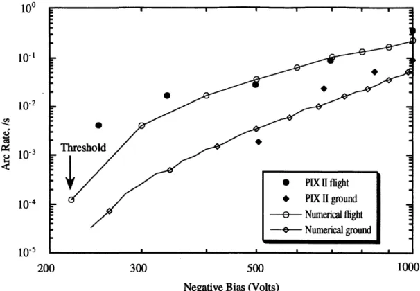
experiment current threshold is then divided by the experiment time to yield the arc rate. Because of the random selection of the parameters from the distribution functions, different arc rates are obtained each time the experiment is simulated. Simulating the experiment one hundred times gives the maximum, minimum, and average expected arc rates for the experiment. Cho and Hastings used this procedure to calculate the arc rate numerically for the PIX II ground and flight experiments. The results showed excellent agreement with the experimental data, as shown in Fig. 2.5.
2.2
Proposed Arcing Mechanism for WTC Cells
As discussed in the introduction, the new WTC cells differ from the conventional geometry cells in that their interconnectors are not exposed to the ambient plasma but are imbedded underneath the substrate. The purpose of this new geometry is to eliminate the current emitted from the conductor, thus hindering the arcing process. However, these cells have been observed to arc during ground experiments [33]. In this design, a semiconductor (the solar cell) is exposed to the ambient plasma along the edge of the cell, as seen in Fig. 1.2, and may aid to the arcing process. A mechanism through which WTC cells arc has been proposed by Font [10]. This arcing mechanism is illustrated in Fig. 2.6 and can be
summarized as follows:
(1) The ambient ions charge the front of the coverglass and the substrate between the cells. The region of the substrate immediately adjacent to the cell is charged to a significant positive potential by the ions, creating a large electric field near the junction of the cell and the substrate.
(2) The electric field becomes significantly large to induce the enhanced field electron emission (EEFE) from the solar cell. Due to the potential structure in the gap, the emitted
electrons will strike the substrate causing the release of secondary electrons and the electron stimulated desorption of neutrals adsorbed on the substrate's surface.
(3) The secondary electrons will be unable to climb the potential well and will remain in the vicinity of the substrate. When the neutral density is sufficiently large, ionization and arcing will take place if the electrons do not become space charge limited and halt the EFEE emission.
Charging of
substrate by
rtion
ions
, b d to Stential , UWFIIbsfitve -75 -30 -1:em
sdon
Charging of
s a substrate by
Fge EFEE and SEE
electrons
I OF jee::::: OF em ssion Ss e ionization Ge
etraon discharge SasubstrateChapter 3
Experiment Descriptions
The SAMPIE and HVSA experiments have been designed to study the interaction between high voltage solar cells and the ionospheric plasma environment. The objectives and oper-ations of each experiment will be described in this chapter.
3.1
SAMPIE Description
SAMPIE, the Solar Array Module Plasma Interactions Experiment, was designed to study the arcing behavior and current collection characteristics of different solar cells and materials likely to be exposed to the LEO environment in future missions. SAMPIE was developed at the National Aeronautics and Space Administration (NASA) Lewis Research Center and sponsored by the NASA Office of Aeronautics and Space Technology (OAST). The flight experiment was flown on board the Space Shuttle Columbia in the STS-62 mission launched on March 4, 1994. The Orbiter was placed in a nearly circular orbit with the following orbital parameters: GMT: 1994+70+04:07:59 Apogee altitude: 307.75 km Perigee altitude: 299.14 km Inclination: 38.920 M: 352.640 Right. Ascension: 204.670 Argument of perigee: 47.370
The seven main objectives of the SAMPIE experiment were the following [19]
(1) Measure arc rates and strengths for selected solar cell technologies and determine the arcing threshold
(2) Measure the plasma current collection characteristics for the selected solar cell technologies.
(3) Verify different arcing mitigation techniques previously demonstrated in ground tests. (4) Study the effect of exposed area on current collection through the design of simple metal/insulator geometries.
(5) Study the dependence of arcing threshold, arc rates, and arc strengths on the properties of the metal interconnector.
(6) If time permits, study basic phenomena related to arcing through experiments on materials such as anodized aluminum and Z-93 thermal control paint; these materials will be used in the Space Station.
(7) Obtain the plasma and environmental parameters necessary for data reduction and analysis.
3.1.1 Diagnostic Instruments Description
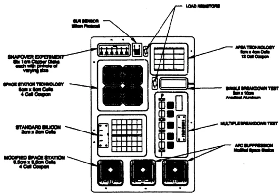
The Hitchhiker-M carrier configured for the OAST-2 mission, with the SAMPIE package on one of the four top mounting positions, is shown Fig. 3.1. As shown in Fig. 3.2, the plate containing the cells to be biased was mounted on top of the metal box, while most of the instruments and electrical subsystems were placed inside the box. A pressure gauge was also included to measure the background pressure. The gauge could measure ambient pressures from 10-7 Torr to 10- 3 Torr. Two high voltage power supplies (HVPS-1 and HVPS-2) in the electronics box biased the specified cells to predetermined dc voltages, ranging from +300 V to -600 V, above that of the Orbiter. In addition, an electrometer in the HVPS-1 circuit measured the currents collected and a sun sensor located on the experiment plate confirmed the attitude of the Orbiter. Two additional electrical probes were also part of the package: a Langmuir probe to monitor the plasma density and temperature, and a V-body probe to monitor the shuttle's potential with respect to the plasma. It was estimated that SAMPE would disturb the ionosphere within an area of one meter in all directions [19], and consequently these probes were positioned about five feet away from the box, shown in Fig. 3.1.
3.1.2 Individual Experiments Description
A layout of the experiment plate is shown in Fig. 3.3. In addition to the individual experi-ments, a sun sensor was used to confirm the Orbiter's orientation.
V-Body Probes
P UEWIT PLATE ASUMLY ENCLOGUA CUMER CAROD CAE LANGMUM PROBW MOUNAI MACKETS ND PLATE ASBEMILY SlHfALCONDoiONER
Figure 3.2: The SAMPIE Electronics Box and Sample Tray
SPACR
I
WAhgabaIOLOU
A-POlrA -- O0n
Figure 3.3: The SAMPLE Experiment Plate
In the experiments, different technologies and arcing mitigation strategies were tested. A detailed description of all the experiments is given in Ref. [20]. Among the cells tested was a four cell coupon of 8 cm by 8 cm wrap-through-contact cells to be used on the International Space Station Alpha, a coupon of twelve 2 cm by 4 cm thin Advanced Photovoltaic Solar Array (APSA) cells, and a coupon of four traditional 2 cm by 2 cm silicon solar cells used to provide a baseline for comparison.
The Space Station (SS) cells were designed to operate in LEO at a nominal voltage of -160 V. The cells are mounted on a flexible substrate, and the inter-cell connections are made through copper traces imbedded in the substrate and welded to the back of the solar cells. The coverglass, semiconductor and substrate of these cells were each 203 p m (8 mil) thick,
and there was only about a 0.81 mm separation between adjacent cells. The semiconductor is silicon, the substrate is Kapton, and the coverglass is ceria-doped microsheet (CMX).
The APSA cells, built by TRW, presented a thinner silicon cell design. Their reduced thickness, 63.5 /um (2.5 mil), is expected to yield mass savings in future space applications. The thicknesses of the CMX coverglass and the Dow Coming adhesive DC-93500 are 51
/tm (2 mil) and 76 pm (3 mil) respectively. The interconnector between these cells is silver
plated invar.