Characterization and Connectorization
of Optoelectronic Neural Probes
MASSACHUSETTS INSTITIEIT
by OF TECHNOLOLGY
Jennifer Selvidge
JUN 08 2015
Submitted to the
Department of Materials Science and Engineering
LI8RARIES
in Partial Fulfillment of the Requirements for the Degree ofBachelor of Science at the
Massachusetts Institute of Technology June 2015
2015 Selvidge All rights reserved
The author hereby grants MIT permission to reproduce and to
distribute publicly paper and electronic copies of this thesis document in whole or in part in any medium known or hereafter created.
Signature of Author... Signature redacted
V--- Department of Materials Science and Engineering May 1, 2015
Signature redacted
C ertified by...Polina Anikeeva Assistan Professor in Materials Science and Engineering
1
A Thesis Supervisor
Signature redacted
A ccepted by ... .. .. / . ...17 ... . ..
Geoffrey S. Beach Department of Materials Science and Engineering
Characterization and Connectorization
of Optoelectronic Neural Probes
by
Jennifer Selvidge
Submitted to the Department of Materials Science and Engineering on May 1, 2015, in Partial Fulfillment of the Requirements for the Degree of Bachelor of Science
Abstract
Reliability of interfaces between the nervous system and the neuroprosthetics can be significantly improved through the use of flexible polymer and polymer composite neural stimulation and recording systems. Furthermore, recent advances in optical neural stimulation methods would benefit from seamless integration of optical waveguides into neural probes. In this thesis, we describe electronic and optical characterization of polymer-based probes produced through thermal drawing process. Our results indicate that polymer-based fiber-probes maintain low-loss optical transmission even in the presence of 90-270* bending deformation with radii of curvature as low as 500 pim over multiple deformation cycles. These probes were robust enough to chronically function in the brain of freely moving mice. Furthermore, these flexible devices enabled direct optical stimulation in the spinal cord, which for the first time allowed for direct spinal optical control of lower limb muscles. In addition to optical characterization, we have developed a method for high-throughput connectorization of the fiber-probes with microscale features to external electronics. This required the development of custom printed circuit boards and involved a multi-step lithographic process. Finally, in a three-months long study we have demonstrated that probes characterized in this thesis yield significantly reduced tissue response in the brain as compared to the steel microwires traditionally used by neuroscientists.
Thesis Supervisor: Polina Anikeeva
Table of Contents
1 Introduction 5
2 Results and Methods 9
2.1 Materials Selection and Thermal Drawing of Fiber Probes 10
2.2 Optical Characterization of Fiber Probes 15
2.2.1 Methods 19
2.3 Multielectrode Probes Magnetic Microconnects 23
2.3.1 Materials Selection 24
2.3.2 Magnetics Characterization 25
2.3.3 Photolithographic Processing of Custom Circuit Boards 29
2.3.4 Methods 31
2.4 Evaluation of Tissue Response to the Implanted Fiber Probes 37
2.4.1 Methods 39
3 Conclusions 41
4 Bibliography 45
List of Figures 1.1 2.2 2.3 2.4 2.5 2.6 2.7 2.8 2.9 2.10 2.11 2.12 2.13 2.14 2.15 2.16 2.17 2.18 2.19 2.20 2.21 2.22 2.23 2.24 2.25 Fig 1 Fig 2 Fig 3 Fig 4 Fig 5 Fig 6 Fig 7 Fig 8 Fig 9 Fig 10 Fig 11 Fig 12 Fig 13 Fig 14 Fig 15 Fig 16 Fig 17 Fig 18 Fig 19 Fig 20 Fig 21 Fig 22 Fig 23 Fig 24 Fig 25 5 9 11 11 12 13 14 15 16 17 20 21 22 25 25 26 26 27 27 29 30 31 35 37 38
Introduction
Optical Neuromodulation Devices: Materials Challenges and Opportunities
Many neurological disorders and pathologies would benefit from more effective treatment options. For example, spinal cord injuries have limited treatment options that do not allow patients to regain full functionality. Others, like depression, are not yet fully understood. In order to improve treatment options for neurological and psychiatric conditions, it is critical to gain a better understanding of neuronal communication in the spinal cord and brain.
This research can be effectively carried out using the
ChR2
470
nm
newly developed field of optogenetics [1,2], which enables temporally precise optical modulation of neural activity. Because the stimulus is optical, it allows one to simultaneously measure the electrochemical neuronal response. This is not possible when using electrical stimulation because the stimulus interferes with the Figure 1: Channelrhodopsin 2. recording. The field of optogenetics relies upon light Light of wavelength 473 nmstimulates the channel to open sensitive ion channels and pumps from archaeal and bacterial allowing sodium ions to rush
in stimulating the neuron to origins (e.g. Channelrhodopsin 2 (Figure 1), ChR2) [4,5], fire. [3]
which enable neuronal sensitivity to visible light.
This new technique resulted in extensive biological applications for optical waveguides and fibers previously used predominantly in the telecommunications industry. There are currently a variety neural probes that include optical stimulation capabilities [6,7]. These devices are typically made of silica and silicon, and since both silica and silicon are extremely
hard and brittle (young's modulus = 73.1 GPa and 150 GPa, respectively), they do not integrate well with neural tissue which has a modulus between 500 kPa and 1 MPa [8,9,10,11,12]. Recent work suggests that this elastic modulus mismatch results in increased foreign body response (glial scarring) and neuron death within the neural tissue in the vicinity of the device, both of which reduce the probe's ability to function over time [13, 14]. Furthermore, the optical fibers based on silica or silicon are simply not mechanically flexible and robust enough to withstand strains up to 10%, which are common in the spinal cord, which would yield their failure upon implantation [15,16].
Soft polymer waveguides, with high tolerance for bending deformation and lower young's moduli, would improve the biocompatibility and allow for chronic delivery of optical stimulation to both the spinal cord and the brain. It is necessary that, in addition to being able to withstand the repeated deformation in the spinal chord and successfully bio-integrate with the surrounding tissue, these chronically-implanted optical waveguides should maintain low-loss light transmission while being actively deformed and after many successive deformations.
Electrophysiological Recordings: Achieving Scalability
Neural signals are carried through electro-chemical potential gradients (action potentials), so neuronal activity is often monitored through measuring electrical potentials in the brain. Therefore, neurobiological studies benefit from simultaneous electrical recordings during optical neural stimulation. In order to characterize the response to a stimulus across multiple neurons, many electrically independent recordings must be taken simultaneously and over time across many locations. Existing probes have often been limited by the use of high modulus materials [13, 14], which produce significant damage to soft neural tissues and evoke strong foreign-body
response. Polymer metal composites could address the mechanical challenges of neural interfaces, while effectively isolating the electrodes from one another. Another critical component for recording devices is their ability to interface easily and effectively with external circuit elements. In the case of multielectrode probes, it is important that high yield manufacturing processes can be established in order to interface these devices with external circuitry, which has previously been a limiting factor [17].
The fiber-based devices considered in this thesis comprise of electrodes as small as 5 Pim in diameter, making traditional wirebonding process (resolution ~ 90 pm) unsuitable for the connection of the fiber probes to the external printed circuit boards (PCBs). Consequently, the microwires within fiber probes are individually connected to the PCBs with silver epoxy, which often results in short circuits. A high yield process therefore is needed for these probes to be used as multifunctional tools for neuroscience research. In order to address this pressing need, in this thesis a new technique using self-assembling magnetic micro-connects has been proposed. Previous studies have shown that magnetic microparticles will self-assemble into a columnar structure in the presence of a magnetic field gradient, and that these columns can form isolated electrical contacts between metal pads, separated by an epoxy matrix [18, 19, 20].
Thermal Drawing Process.
The probes characterized and connected in this study were fabricated via a thermal drawing process [21, 22, 23, 24, 25]. During fiber drawing, a perform, which is a macroscale template of the fiber with matching cross-sectional geometry, is heated above the glass transition and melting temperatures of all the constituent materials and stretched. During the drawing process, the stress is carefully controlled through use of multiple heating zones within the furnace of a drawing
tower, as well as the feed speed of the preform and the rotational frequency of the capstan wheel via which the fiber is collected. The drawing process produces hundreds of meters of fiber with microscale features with a cross-sectional pattern exactly matching that of the preform [26]. While traditionally applied to glasses, recent advances in multi-material fiber technology spear-headed by Fink lab at MIT enabled drawing of polymers and composites. In the Anikeeva group, we have taken advantage of these fabrication advances to create a palette of flexible polymer-based fiber-polymer-based probes for recording and modulation of neural activity in the brain and spinal cord. This thesis describes my contributions to characterization of several types of fiber-based neural probes. Furthermore, I detail the high-throughput connectorization procedure that I have developed to enable robust interfaces between these fiber-based devices and conventional electronics.
Results and Methods
Materials Selection and Thermal Drawing of Fiber Probes
Polycarbonate (PC) and cyclic olefin copolymer (COC) were chosen to form the waveguide and cladding as they have lower Young's moduli than silica-E = 2.38 GPa and 3.0 GPa respectively-making improving their bio-integration from silica and silicon. This combination of polymers also transmits light effectively in the visible range due to their low absorption in this range and the difference in their refractive indices (Figure 2).
S0.8
ChR2
Excitation
Peak
E
oL4
0 C-
0.2
PCfiber
- - -PC/COC
fiber
PC/COC/CPE fiber
0.0
400
40
500
50
600
60
70
WaveWenh (rwn)
Figure 2: Transimission of PC, PC/COC, and PC/COC/CPE fibers. Close to 100% transmission is observed at the absorption peak of ChR2 [27].
PC has a refractive index of n = 1.58 and COC has a n =1.52 [28, 29, 30]. This means that at incident angles greater than or equal to.74.2* the total internal reflection criterion is satisfied, and none of the light will escape the PC optical core. At incident angles smaller than
this, some light will be escape out the sides of the waveguide, but much of the light will still be reflected internally. Snell's Law states that:
n1 sin 6, = nzsint
where ni is the refractive index of the waveguide core, n2 is the refractive index of the waveguide
cladding, 01 is the incident angle of the light against the interface and Ot is the angle of the light the crosses the boundary into the cladding and determines the total internal reflection angle. The maximum coupling angle, another important optical fiber descriptor, represents a cone within which light coupled into the fiber will propagate and total internal reflection will be satisfied. Similarly where n is the index of the medium the light is coming, and 0 from the maximum coupling angle is:
n2 -n2
6 = arcsin( 1 2 n)
For these devices the maximum coupling angle from air is 25.50. This descriptor gives rise to another common waveguide descriptor, the numerical aperture, NA.
22
N A= n - n
The value for this system is NA = 0.43. The refractive indices of these materials allow them to be drawn into effective waveguides, as demonstrated by the numerical aperture, maximum coupling angle, total internal reflection criterion angles. Additionally, their mechanically properties help the devices to integrate minimally invasively with the surrounding tissue.
In order to create our all polymer optical devices, a thermal drawing process was employed. A perform-a template containing all the desired features and matching the intended
final cross sectional geometry but many times larger and with a correspondingly reduced length-was made. For the optical fibers a rod of PC was wrapped in COC sheets and annealed under vacuum to eliminate air pockets. The resulting composite rod was then machined to form
CPE4
Figure 3: Manufacture of the preform. For the spinal cord devices a PC rod was wrapped in sheets of COC and then machined to make channels for the electrodes. After the CPE blocks for the electrodes were inserted, the entire structure was wrapped in a sacrificial layer of PC that for the spinal cord devices was etched off after drawing using dichloromethane.
two slots along its length. Conductive carbon black doped poly(ethylene) (CPE) blocks were then put into these slots in order to create electrodes. The entire structure was then wrapped in a sacrificial layer of PC and annealed under vacuum to create a single solid rod preform, free from gas bubbles along the length (Figure 3).
Following the creation of the preform, the annealed rod was placed into a fiber drawing tower (courtesy of Prof. Fink and his team) heated to above the glass transition temperature of all the materials and high stresses were applied to the system via spinning capstan in order to ing. The maerials ere theaed create hundreds of meters of fiber with the same cross tempe atures,their gla tranap d sectional geometry but many times smaller (Figure 4). stresses were used to create the fibers. These fibers were then etched using dichlormethane to
remove the sacrificial polycarbonate layer.
Several cross-sectional geometries have been fabricated for use in the brain and spinal cord (Figure 5). The spinal cord device, Figure 5A, was designed to be as thin as possible so as to maximize its optical performance in extreme mechanical environments. The two brain probes, Figures 5B, has both been modified to allow for drug delivery through the introduction of two hollow channels.
A
Figure 5: Optical microscopy images of cross sections for neural probe devices. A is for the spinal cord, whereas both B is for the brain. In brain devices, unlabeled rectangular channels (B) are hollow drug delivery channels. The scale bar in A is 50 microns [17, 27].
Like the optoelectronic probes, the high-resolution multielectrode probes need to be stable upon implantation and to minimize adverse affects to the tissue, while maintaining their efficacy as recording devices. In order to address these concerns, the fibers comprised of tin electrodes within polyetherimide (PEI) matrix were created through the same thermal drawing process [17]. The PEI was used both to insulate the individual electrodes from one another, while maintaining a relatively low effective young's modulus of the whole system (PEI Young's modulus is ~ 3.04 GPa as opposed to the modulus of Sn ~ 50 GPa). In order to minimize the electrode size, the fibers were created using a thermal drawing processes with the optical probes, but drawn twice as shown in Figure 6. In order to manufacture the preform a hole was drilled through a rod a PEI.
A tin rod the size of the hole was then inserted. This system was annealed and de-gassed under vacuum. This preform was then drawn above the glass transition temperature of PEI and the melting point of Sn using controlled mechanical forces in the drawing tower. A rod of poly(phenylsulfone) (PPSU) was then machined to have a hole along it's length and sections of the drawn Sn-PEI fibers were inserted into the hole. This probe was again annealed under vacuum to form one solid rod without gas bubbles. After the annealing process for the new preform, it was drawn above the melting temperature of Sn, and glass transition temperatures of PPSU and PEI. This process yielded fibers with the cross sections shown in Figure 7, and these fibers were then selectively etched to remove the sacrificial layer of PPSU.
Heat
Figure 6: Thermal Drawing process for the multielectrode probes. By drawing twice and etching the excess off, a very small cross section was created for the probes.
Figure 7: Cross sections of tin PEI probes, etched and unetched with a sacrificial layer of PPSU removed through selective etching. The Sn electrodes are surrounded by a PEI matrix.
In recent publications, it was demonstrated that fibers described above enable chronic stimulation and recording of neural activity in the brain and the spinal cord [17, 27]. Although the multielectrode probes proved very effective for recording achieving high signal-to-noise ratios and evoking negligible tissue damage, the current methodology for interfacing them with the external circuitry is very difficult and impedes their wide use by the neuroscience community.
Optical Characterization of Fiber Probes
The optoelectronic fiber-probes were mechanically deformed in order to characterize their optical behavior under bending deformation. It is important for the devices to remain functional after acute bending, e.g. if a fiber probe were to be wrapped around an animal's vertebrae, and also after repeated bending that would occur over a lifetime of a freely moving mouse
chronically implanted with a fiber-probe within its brain or spinal cord.
100 The results of the acute
go ... 1800 multi-radii bending studies
0 -70
. for the spinal cord devices
-1 - are shown in Figure 8. For
T...-both the 900 and the 1800
trials, plateau like behavior,
20 --- --- increasing slowly towards
270* IO
:1- 0100% transmission at the
0-0 2 4 6 8 10 12 14 16 larger bending radii is
Radius
of
Cuvatre
(nm)
Figure 8: Transmission as a function of bending radius for observed. For all the angles, a
spinal cord devices. steep drop off is observed in
transmission for radii of curvature between 1 mm and 0.5mm. It is important to notice that fiber, when bent to 2700 falls off more steadily than the other two angles.
Figure 9 shows the results of the acute multi-radii studies for the brain optoelectronic probes. A clearly marked decrease in the light output is observed for the smallest radii (1mm) measured. For the brain, only 90' bending trials were conducted due to the different mechanical environment than the brain probes would experience in vivo.
1.0-0.8 0 0.6- CD0.4- :20.2-0.0 0 2 4 6 8 10 12 14 16
Radius of curvature (mm)
Figure 9: Transmission as a function of bending radius for device 1B with 900 bending. The steep decrease that was observed in the spinal cord devices was also observed in the device I B brain devices.
The brain and spinal cord devices behave consistently for 90' bending deformation, in that both have plateau like behavior followed by a steep drop off at smaller radii. Both show a low loss plateau at larger radii of curvature and then a steep decrease in transmission at the smaller radii, which is consistent with the understanding that the devices stop satisfying the total internal reflection condition. It is also important to note that the sharp decreases in the data in the 900 studies for both the spinal cord and brain probe correspond to the point where plastic deformation of the samples began to occur. This was observed empirically as the fibers were permanently bent and did not assume their original conformation at these points as they did after
being bent at the larger radii. It seems likely that due to the plastic deformation, the waveguide properties changed due to the drastically increased defect density at the deformation points.
Figure 1OA shows the results of the cyclic deformation characterization of the spinal cord device and Figure lOB shows the results of cycling deformation characterization for brain device. Both show no significant decrease in light output over the lifetime of the test.
A o B 12
Avov
- 0.6-0.4I0
21 020.2-0.0o- - 0.0 2 4 a00 4 11a IIa 2
2 4 6 8 10 12 14 cyce number
OcIe(#)
Figure 10: (A)Light Transmission as a function of cycle number in the spinal cord device. The black line represents the average and the gray area represents the error. No appreciable drop off is observed, implying that changes in light output in the bent state are due to scattering effects and not permanent damage to the device. (B) Light Transmission as a function of cycle for device 1B. The blue line represents the average light transmission and the shaded yellow area represents the standard deviation. Moderate optical heating effects were observed in these samples, so this data has been normalized over the light output increase in an unbent device for 30 minutes, the time taken to complete each run. No significant losses are observed, as with the spinal cord device, so variation between the bent and unbent states can be attributed to scattering.
The multi-radii and repeated deformation studies for the optical probes suggest that these devices can function in chronic studies in vivo. Both types of fiber probes are able to transmit light while bent, and their light output is not diminished during repeated deformation. Above a critical bending radius of 1 mm for the spinal cord probes and 2 mm for the brain probes, close to full transmission was observed at 900 deformation (also at 1800 for the spinal cord probes). It is
important to note that this radius corresponded for both to the point of plastic deformation of the fibers. To function in an awake and freely moving mouse chronically it is extremely important that the devices continue to function while bent and after repeated deformations; these studies showed that this is indeed the case. They also demonstrated that were the tissue to bend, such as in the spinal cord, the device would be able to bend as well. Although there is still a modulus mismatch between the modulus of neural tissue cord tissue (between .5 and 1 MPa) [15, 16], the decreased stiffness as compared to silica fibers, makes them more likely to deform somewhat similarly to the tissue, and therefore less likely to cause damage. These studies showed that the devices were indeed capable of this deformation, unlike silica, which is promising for bio-integration purposes.
Methods
Sample preparation
The optical performance of optoelectronic fibers in response to mechanical stress was analyzed using a laser with wavelength k = 473 nm, the optical absorption peak of channelphodopsin 2 (ChR2) [1].
Following thermal drawing, the devices were prepared for testing by a series of post processing steps. Because the draw is more stable using larger geometries, a sacrificial layer was added in order to stabilize the draw [17, 27]. In order to remove the sacrificial layer and achieve the small structure desired, the spinal cord devices were etched for 1-2 minutes using dichloromethane. In order to ensure optical coupling with the brain devices, no etching is done. Zirconia ferrules were attached using optical epoxy to the spinal cord devices and steel ferrules were attached to the brain devices. After curing, the ferrules were polished with silicon-carbide grinding paper of grits 120-4000 to ensure good coupling from the silica waveguide that was used to direct the laser light into our devices for these tests. Index matching fluid was used for the brain studies in order to improve coupling to the silica fiber carrying the light from the laser.
Multi-Angle Bending Deformation
The fibers were bent on a plastic guide shown schematically in Figure 11. The spinal cord device probes were bent to eight bending radii, 0.5mm, at 90', 1800, and 2700, using 12.5 cm devices. The brain probes were bent to 900 only because the brain is a much less intense mechanical environment than the spinal cord. The brain device samples were bent to 1.0mm 2.5 mm, 5 mm, 7.5mm, 10mm, 12.5 mm, and 15 mm. The fiber was held down by hand in the tracks milled into a plastic mold so that the deformation was repeatable across different fibers. Each
fiber would be bent from the largest radius to the smallest, straightening the fiber between each and measuring the light output before each bend in order to renormalize, and cutting the fiber after plastic deformation occurred.
Repeated Deformation
Figure 12 shows a schematic of the bending test set-up. The device was placed between Figure 11: Schematic of bending guide.
Fibers were laid on machined tracks allowing two plates, one stationary and one an X-Y them to be consistently bent, in a repeatable
manner. Three measurements were taken for stage, which allowed for repeatable each device at each radius (not shown) by
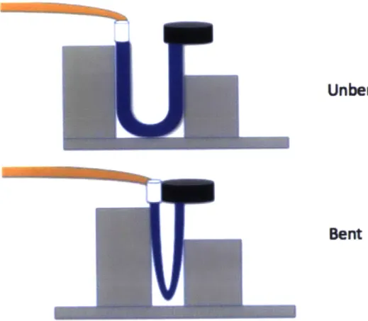
shifting the position of the fiber in the guide. deformation in the x direction. A photodetector was placed above the stationary plate and a piece of paper with a small hole was used to guide the waveguide to its surface and block any outside light. The waveguide was attached to both plates using tape in order to not damage the waveguide in the attachment process. Both the spinal cord device and brain device were characterized using this set-up. The devices were bent to a radius of curvature of 2.5 mm for the spinal cord device and 3 mm for brain devices at 1800 in the deformed state, respectively. Device IB was measured on 15 cycles and the spinal cord devices were measured on 20 cycles of deformation and relaxation. The brain device measurements were normalized over the unbent fiber light output over time, because some heating effects were observed and the laser changed in intensity slightly over time, causing the fiber to seemingly become more and more transmissive.
Unbent
Bent
Figure 12: Schematic of cycling set up. The blue feature in this diagram represents the waveguide. The device was moved repeatedly from a less bent position serving as the unbent state to the bent state and back again, using an X-Y stage to maintain positional accuracy. This was done 15 times with measurements being taken at both the bent and unbent states,
but not dynamically as the device moved.
Creation of Optoelectronic Implants
The implant-ready optical devices can be seen in Figure 13. The fiber can be seen in both the brain and spinal cord optical probes attached to the ferrule (ceramic for the spinal cord device and steel for the brain device). Although it was not explicitly discussed in previous sections, these devices also had the ability to record basic electrical signals, which the copper wires and
printed circuit board allowed for. The copper wires were connected with conductive silver paint and attached using medical grade epoxy. Although the actual implants were connectorized to be
multifunctional, the devices used to conduct the deformation studies had not been and were simply sections of each type of optical fiber attached to a ferrule.
Figure 13: Finished optical probes for both the spinal cord (top) and brain (bottom) devices. The optical fiber can be seen coming out of the ferrule in both cases. Copper wires connectorized the electrodes in these devices, and the brain device included drug delivery tubes.
Multielectrode Probes Magnetic Microconnects
In order to optimize the multielectrode probes as a neuroscience tool it is critical to effectively connect them to the external circuitry. This has previously been accomplished by attaching each individual electrode to a printed circuit board. However, this process is not sustainable for larger scale use of these probes or for high electrode-count devices, and an easier, more streamlined process must be developed. In order to address this problem, we have investigated the use of self-assembling magnetic micro-connects within an epoxy matrix. This methodology, once optimized, would allow for the simultaneous connection of the electrodes to photolithographically patterned chips.
To develop the magnetic microconnects, it was first essential to understand the basic materials physics underlying the alignment of magnetic microparticles placed in magnetic field gradient within a viscous medium. When the particles are randomly dispersed within the liquid epoxy and in the presence of the magnetic field they are affected by the following forces: the magnetic force resulting from the magnet, the earth's gravitational pull, the magnetic interactions between the particles from their induced magnetic dipoles, and the drag force while they are moving due to the fluid matrix. The total force on each of the particles is a sum of these four distinct forces. When there is no magnetic field, the particle falls under the influence of gravity where m is the mass of the particle, and g is the gravitational pull of the earth. As the particle falls the epoxy exerts a frictional force on it, expressed in terms of the radius of the particle, r, the viscosity of the epoxy qj, ands the velocity of the particle Vp. When the magnetic field is applied the particle is pulled along the gradient of the field B and the magnetic moment of the particle, ji. The particles also interact withon another magnetically, following Ampere's law, in
which the change of the current, I., on each of the particles and the distance between the particles determines the strength of the overall force.
Ftotal = Fmag + Fdrag + Fgravity + Fmagnet
Fdrag = 6Trij'V, a mag,12
ffdl
2x(dllx aR12) Fma_,72 = ff/ R12 C1 C2 Fgravity = mg Fmagnet V ( )Balancing these forces seems to make the case for larger particles and stronger magnetic fields (and therefore greater induced magnetic forces within the particles). However, prior research has also indicated that, for smaller pad sizes, the use of larger particles results in higher failure rates,
as the particles approach the dimensions of the pads themselves and then form larger, more
disperse columns [19].
Materials Selection
In order to create the magnetic micro-connects it was necessary to choose an epoxy matrix, choose a type of microparticles, and to determine the optimal concentrations within this mixture. Microparticles composed a nickel core (81% of total weight) and gold coating (19% of total weight) of size 2.5 microns (BRIGHT 19GNM2.5-NiD from Nippon Chemical and Industrial Co.) were chosen in order to satisfy the size requirements for small pad sizes and the systems requirements that they be magnetically active and also highly conductive. Two UV-curable epoxies were chosen and tested for their fitness as matrix agents due to their relatively low viscosities of 0.4005 Pa(s) (epoxy 450) and 0.5785 Pa(s) (epoxy 650) in order to maximize the
particle active distance. By choosing a low viscosity matrix, we reduce the drag forces experienced by the particles, which may facilitate the particle alignment with the field gradient.
UV cure epoxy was desirable as the light source could be easily repositioned if necessary and the epoxy will not cure until it is exposed to UV light, which would have otherwise limited the experiment lifetime to the curing time of the epoxy.
Magnetics Characterization
Figure 14: SEM, no magnetic field exposure, sat for 30 minutes before UV exposure.
Figure 15: SEM image Higher viscosity epoxy with 25 wt % solid content.
In epoxy 450, without the presence of a magnetic field, the beads did not stay near the surface of the epoxy, which is important if the beads are intended to form electrical connections between two surfaces (Figure 14).
However, in the presence of a magnetic field of approximately 0.6 T with gradients of 40 T/m and across concentrations from 25-35 wt % in both epoxies, the beads did not sink through the solution and some number instead stayed at the surface of the droplet which made it possible to image them using a scanning electron microscope (SEM). Upon comparison between of the epoxy 450 and the epoxy 650, it was determined that the
epoxy 450 epoxy produced better structures for the purposes of this research. Even at the lowest concentration, the structures formed by the epoxy 650 were similar to the one shown in Figure
15. These structures show large amounts of agglomeration connectivity in the x-y plane, which
was determined to be suboptimal for the intended application due to the possibility that such connections would not remain electrically isolated.
Figure 16: SEM image, 450 epoxy 25 solid wt%.
superimposing cross sectional SEM images of the fibers and
Figure 17: SEM image 30 wt% solid content epoxy 450, 2 hours magnetic exposure.
In the epoxy 450 all the microbeadss appeared to be more evenly dispersed in the x-y plane, however, 25% solid weight (Figure 16) was determined to be insufficient to produce the desired density of contacts. This was determined by the particle arrangements. If, based on manipulation of these images, it seemed like there were numerous orientations were very few or no electrodes would be in contact with a bead, the concentration was determined to be too sparse. However, even at
25% weight solid content, it is
are forming small potentially columnar aggregates.
The optimal concentration of microbeads was found to be
approximately 30% weight solid content (Figures 17, 18), as higher concentrations, much like with the more viscous epoxy, formed highly interconnected structures in the X-Y plane, Figure18: SEM image, 3 hours magnetic exposure,
vigorous mixing, 30 wt% solid content, epoxy 450. which would yield electrically shorting the neighboring electrodes onto one another.
Cross sectional SEM images of the cured composites (30 wt % microbeads in epoxy 450) on silicon revealed a columnar structure (Figure 19) with clear directionality.
We have also assessed different mixing methods for dispersing the magnetic beads within an epoxy matrix. Manual mixing produced most promising results, as no other mixing method yielded structures with microparticles near enough to Figure 19: Cross-sectional SEM of magnetic bead columns.
While in our earlier studies, we have employed a manual process for electrically connecting multielectrode probes to external PCBs, one of the goals of this thesis was to create a scalable connectorization methodology. By performing the experiments described in this section, it was determined that the epoxy 450 was suitable for the intended application. We hope that by using a low viscosity epoxy the agglomerations will be evenly dispersed through the matrix and this appears to be the case from preliminary studies. It was also determined that the longest magnetic exposure times resulted in the best dispersion of the particles. These evenly spread particles, we hope, will allow us to connect the metal on the device surface and the metal on photolithographicaly patterned chips. Studies of several different mixing methods determined that the most promising was mixing vigourously for several minutes using a blunt tool such as the end of the needle cap, and that exposing the mixture on the magnet by an hour longer before curing produced better results than those produced by other methods. It was also confirmed that 30% solid weight mixtures performed best, as was expected based on prior reports [18, 19, 20]. In order to characterize the magnetic interconnect process, cross sectional SEM images were also obtained in the direction orthogonal to the substrate surface. SEM imaging provided evidence that the agglomerating microparticles were forming columnar structures as had been shown by others in the field [18, 19, 20]. These columnar structures have the potential to provide isolated conductive pathways.
Photolithographic Processing of Custom Circuit Boards
In order to allow for wide spread use of the multielectrode probes as neuroscience tools, it is necessary to create an easy repeatable process. One such step in that is to create a tailored interface for the fibers that will allow for simultaneous connection of all the fibers, without changing the cross section, such as by splitting the electrodes. A standard way for creating such individualized circuit interfaces is through a photolithographic process. To this end, chips were designed and processed for testing purposes.
Figure 20: SEM image of photolithographically patterned chip, matching the cross-sectional geometry of one of the multi-electrode probes.
The photolithographically patterned chips (Figure 20, 21) showed gold deposited on silicon in the desired pattern and that the etching process etched a hole in the desired location. The success of these chips implies that it will be possible for the interfacing to be done through standard, well characterized processing methodologies.
The chips successful resolution, means further work can now be done to characterize the effectiveness of the connections along the whole system.
Figure 21: (A) SEM image of photolithographically patterned chip, matching the cross-sectional geometry of one of the multi-electrode probes. The black circle is one of the etched holes with the intent that a waveguide could pass through.
Methods
Mixture Characterization
Figure 22: Set-up of magnetic testing set up. The slide was placed on the magnet and the UV lamp was set up above it so as to be able to cure the system without perturbing it.
Concentrations of 25 solid wt%, 30 solid wt%, and 35 solid wt% were chosen where solid weight is used here to mean the weight percentage of the microparticle-epoxy mixture accounted for by the microparticles. 30 solid wt% was standard in literature [18, 19, 20] and 20% was shown to have a higher rate of failure for small pad sizes [19]. For this reason 25, 30, and 35 solid wt% were chosen. The samples were mixed by hand using a flat edge, typically a needle cap, until it was smooth and appeared consistent. In some cases, the mixture was then sonicated for 30 minutes or mixed with a magnetic stirring plate for 3 hours in order to determine the optimal mixing method. From there, a few drops of the mixture were placed on the center of a glass slide (top-side SEM analysis) or silicon wafer piece (cross sectional SEM analysis), applied by a needle. The samples were exposed to both the magnet and using the set up shown in Figure 22, the samples were exposed to first the magnetic field and then to the UV light. A UV lamp was
affixed 4 inched above a 1-inch cube magnet and the sample was then placed about .2 inches from the edge of the cube magnet in order to minimize cross-fields. The samples were then exposed to the magnetic field in complete darkness for 0 minutes (but allowed to sit for 30 minutes in the dark), for 30 minutes, for 60 minutes, and for 120 minutes. They were then exposed to an 8 Watt UV lamp of wavelength 302nm for 15 minutes while continuing to sit in the same location.
Photolithographic Patterning for Chips
In order to make the chips, a photolithographic quartz and chrome mask was designed to match the cross section of the fibers, with electrically conductive pads matched to each of the
electrodes, wired to conductive pads to be attached to external circuit elements. Once these masks were created, 6 inch p-doped silicon wafers were procured. These wafers were first rinsed in acetone, isopropanol alcohol, and deionized water to clean off particulate matter that may have been on the surface then dried thoroughly. These wafers were then put in an HDMS coater in order to form a thick layer of HDMS to improve resist wetting and adhesion through
hydrophobic interactions. The wafers were then placed on a Manual Photoresist Coater (Solitec Inc.Model 5110) (the coater) and a thin layer of AZ5214 image reversal resist photoresist was spun on, using 500rpm for 6 seconds while the resist flowed out of the coater, 750 rpm to spread the resist for 6 seconds, and then spun at 1500 rpm for 30 seconds to create an even coat between
1.2-1.5 microns thick. Image reversal resists are those such that the exposed area stabilizes and
stays after development, whereas the unexposed area comes off. The wafers with HDMS and resist were then baked in a Blue M Model DDC- 1 46C Bake Oven to stabilize the resist at 90'C
EV620 Mask Aligner for 1.7 seconds with the photomask. The wafer was then post-baked for another 30 minutes to crosslink the exposed regions. After this crosslinking, the photoresist was re-exposed, this time for 60 seconds. Then, using 422 Developer, the wafers were developed for 5-10 minutes, in order to resolve the small features, checking using fluoroscope microscopy that this had occurred. Following this the wafers were then cleaned using the spin rinser and put in the asher to be cleaned with oxygen plasma for 15 minutes. This process ensured that the
features were fully resolved. 150 nm of gold with a 15 nm layer of titanium as a binder to help the gold attach was then deposited using an Electron-Beam Evaporator (Temescal Model
VES2550) at a vacuum pressure of 2.0 X 10⁻⁶ Torr. After deposition, the wafers were then put in acetone for 24 hours in order to lift off the photoresist and the unwanted metal with it. After this step, the wafers were exposed to the same cleaning process and HDMS process described above. Another layer of photoresist was then spun onto the wafers, this time using AZ 4612, thick resist. Thick resist is poured onto the still wafer on the coater until it covers the majority of the wafer. The wafer is then spun at 1500 rpm for 1 minute to get a 10 micron thick layer. The wafer and resist are then baked for 30 minutes at 900 C. After the resist has baked, the wafer is then
recoated in the same manner, in order to get a 20 micron thick layer and then the whole system is again baked, this time for 60 minutes. The thick resist is then exposed for 7 cycles of 15 seconds of exposure and 15 seconds of darkness on the mask aligner. The darkness in the cycles kept the resist from bubbling due to excessive energy fluxes, by giving it a chance to cool. After
exposure, the wafers were developed for 10 minutes in 412 Developer. Although the feature size for the second layer was an order of magnitude larger the double thick resist made it important to develop for a relatively long time, in comparison to thinner resist coats with equivalently sized features. The wafer was then attached to a handle silicon wafer, using thick resist in an
alternating pattern of photoresist and bare silicon. This was done in order to optimize both attachment between the two wafers and also thermal contact between the wafer and it's handle. The wafers were bonded by placing the handle wafer on the backside of the chip wafer and pressing down lightly with the backside of a ruler in order to apply even force. The wafer stack was then backed for 60 minutes. The stack was then put in the ICP Deep Trench Etching System
STS -6" plasma etcher, which employs the Bosch process in order to drill straight holes into silicon by applying, at 15 second intervals, alternating etching plasma and deposition plasma depositing Teflon to protect the walls of the hole as organics are attacked significantly more slowly than the silicon by the etching plasma, so the photoresist protected the surface and the Teflon protected the walls of the holes. This process was run for 5 hours in order to drill holes all the way through the 650 micron thick wafer. The photoresist and handle wafer were then
removed in acetone. After the removal, the individual devices were then cut on the Diesaw Disco Abrasive System (Model DAD-2H/6T), using a diamond blade. This process is outlined
A B
C D
-7
77
G H
Figure 23: Photolithographic chip processing. (A) A p-doped 6 inch silicon wafer was cleaned for patterning. (B) The wafer was coated with a 1.5 micron thick layer of image reversal resist. (C) The wafer was exposed to UV light and developed. (D) Electron Beam deposition was used to deposit a 150nm of gold and 15nm of titanium as a binder on the wafer. (E) Acetone was used to lift off the photoresist and unwanted gold. (F) The wafer was then coated with a 20 micron thick layer of thick resist. (G) The wafer was exposed and developed and a handle wafer was attached for the plasma etching process. (H) The wafer was then plasma etched using the bosch procress. (I) Following lift off in acetone, the finished wafer was cut on the die-saw into chips.
Scanning Electron Microscopy Analysis
Scanning Electron Microscopy (SEM) was performed on the magnetically aligned microparticles both top down and in cross section using a FEI/Philips XL30 FEG ESEM. Due to the
non-conductive nature of the matrix material, low vacuum H20 BSE microscopy was performed on
intensity of 5kV. Some samples were imaged laterally and others in cross-section. Those samples imaged in cross section were broken by applying pressure to one edge of the silicon substrate, causing it to crack in a straight line along that crystallographic plane. The epoxy did not break and a razor blade was used to cut it.
SEM was also performed on the photolithographically patterned chips in order to confirm their manufacture. These scans were performed under high vacuum with 15kV beam voltage.
Evaluation of Tissue Response to the Implanted Fiber Probes
Histology experiments were conducted in order to characterize the tissue response to chronic implantation of the multielectrode probes. Existing neural interface devices are been limited by temporally-decaying recording abilities due to poor mechanical biocompatibility. Consequently, reducing the tissue response is very important to improve the chronic performance of neural probes. By characterizing the tissue across several key markers for foreign-body response, it is possible to compare quantitatively the biocompatibility between the current state of the art technology and our fiber-based probes.
Figure 24: Sample confocal image of multielectrode probe implant hole. Image shows DAPI channel in frame E, Ibal channel in frame F, IgG in frame G, and a merged image in frame H.
The histology experiments yielded images such as the one shown in Figure 24. The low immune response can be seen on all the indicators, through the low fluorescence on those channels (Figure 25). These experiments also demonstrated that the multielectrode probes produce significantly (P < 2 x 10⁻⁶) less immune response than the steel microwire after 3 days and a similarly low level of immune response to the steel microwire, after longer time periods.
b c 900 600 700 600 400 300 100. 001 200 600* 60WO 0 0 70 60
Sol
201 10 0 25 20 1100:
-200 -100 0 100 200Distance kom probe Center (Pm)
d OFAP 100 3 days 50 0 50 100 150 200 h e0 3 daos 40 20 0 50 100 1SO 200 f j EDI 10i 0 50 100 150 200 30w1hi 30 1wel W ~ " 20 20 0 50 100 150 200 0 so 100 150 200 5 100 150 200 40 20 0 50 100 150 200 k 30 0 1 2ee 20 10~ 10 0 0 100 150 200 30 20 015 50 1 10 _____________ 0 so 100 150 200 0 50 100 150 200 0 50 100 150 200 0 50 100 150 200 p t q r S 203S 15 1 n 11WH I MOnI ma'nh 1520 4 10 0 0 502 0 50 so 100 10 200 0 50 1 00 10 200 0 so 100 ISO 200 0 50 100 150 20 U 6 3M 6 3m 44 2 2 0 50 100 150 200 0 50 100 150 20
Distanog tom pRobe Inerface (sm) Distance fram probe te0face (Pm)
1.5
1.0
0.5
000 s 100 150 200
DWsAnce from PO 2 .10eO (pam)
w 4 3
nw w
2
0 50 100 150 200
Distance from probe hntalae (Pm)
Figure 25: Confocal images were converted into pixel intensity as a function of distance from the center of the implanted probe. The results shown in d-w show the intensity as a function of distance averaged over 5 trials for both the steel microwire (red) and the multielectrode probe (blue) at various time points.
The studies demonstrating that the multielectrode probes caused a reduced immunological response along several key markers for blood brain barrier breach and glial scarring demonstrates a significant biocompatibility improvement over existing technology. The studies produced results in agreement with prior work that lower moduli materials bio-integrate better with the surrounding tissue [8, 9, 10, 11, 12]. This lowered response potentially corresponds to
a
I
I
I
I
I
ibetter overall performance of the probes in chronic in vivo studies. These probes, due to their improved biointegration could provide a new methodology for neuroscience, especially for studying short-term chronic studies that have previously been hindered by biocompatibility issues.
Methods
In order to test the in vivo biocompatibility of the electrical devices a series of histological studies were conducted. These involved the implantation of the multielectrode probes and of a similarly sized steel microwire into the brain of a mouse and quantifying the tissue response at several different time points. Ten wild type mice were implanted (2 mice per time point of 3 days, I week, 2 weeks, 1 month and 3 months after implantation) with three multielectrode probes and three microwires. After the desired time had passed the implanted animals were anesthetized and sacrificed. The devices were carefully explanted and the brains were removed and sectioned to 50 ptm slices. The slices were then incubated with the desired primary antibodies in blocking solution (goat anti-GFAP, goat anti-Ibal, and rabbit anti-CD68). The primary antibodies were then stained with the desired secondary antibodies conjugated to fluorescent groups (donkey anti-goat, goat anti-rabbit, or goat anti-mouse IgG was conjugated to either Alexa Fluor 488 or Alexa Fluor 633). The slices were then mounted on microscope slides (VWR) [17]. For each sample, the least damaged deep brain slice was selected to image. A map image was taken of the brain slice at 4X in air in order to assist future identification of the implant holes. A lOX image taken in air was also used for this purpose. The analyzed fluorescent images were taken with the same exposure settings on an Olympus FV1000 laser scanning confocal microscope with an oil immersion 20x objective of numerical aperture NA = 1.25. Each
hole was imaged at multiple heights separated by regular intervals and the intensity was compiled over 12 images.
Averaged fluorescent intensities as a function of distance from the electrode-tissue interface for IgG, GFAP, Ibal, and ED 1 were found radially from the center of the implant hole for both the microwire and the multielectrode probe for each time point.
Conclusions
Over the past several years the Anikeeva group has been investigating applications of the fiber drawing process in the design of multifunctional neural probes. While these probes have shown promise as electrical, optical and chemical neural interface tools, much work remains to transform them into empowering tools for systems neuroscience. In this thesis, I have developed fabrication and characterization techniques that allowed us to understand the optical and electronic performance of several classes of fiber probes as well as investigated the tissue interfaces with these devices. Specifically, within the scope of this these I have lead and/or contributed to the following efforts: (1) Optical characterization of fiber-based optoelectronic neural probes for applications in the brain and spinal cord; (2) Development of high-throughput connectorization approaches between the fiber probes and external circuits; (3) Evaluation of tissue response to chronically implanted neural probes.
Optical characterization of fiber-based optoelectronic neural probes for applications in the brain and spinal cord.
To enable optical stimulation in high-strain environments, such as spinal cord, and to reduce tissue damage in the brain polymer-based fiber probes were developed. These devices offered greater flexibility as compared to silica and silicon, and thus allowed for stable optical performance over a period of three months in the brain of awake and freely moving mice [27]. Furthermore, these devices allowed, for the first time, to perform optogenetic control in the spinal cord.
Although less important in the brain than in the spinal cord, the decreased stiffness of these materials and their ability to bend and retain their high light transmission, while potentially doing less harm to the surrounding tissue, should not be understated. In both cases, these fibers
represent an improvement to existing tools. To further to improve the characterization of these fibers, the repeated deformation trials should be re-run for approximately 10,000 deformations rather than 15-20 which would be a more realistic model of the behavior over the whole life of the implant. However, even without this extension, these fibers already pose significant new opportunities for researchers in neuroscience fields to expand their scientific endeavors.
Development of high-throughput connectorization approaches between the fiber probes and external circuits
As previously described, the importance of the external circuit interfacing work should not be understated. In order to truly use the multielectrode probes to their full potential, it is critical that they can be quickly and easily connected to external analog electronic components while maintaining electrical isolation of the electrodes themselves. To date, this has been done by individually connecting each electrode by hand [17]. This effectively limits the number of electrodes and limits the usability of the tool. However, the success of early work using magnetic microconnects, such as the formation of continuous columns in the z direction as was observed in the electron microscopy images implies that such connectivity should be possible. This early success was in agreement with prior work that has shown that these magnetically active microparticles assemble into columnar structures [18, 19, 20]. Future work should be done to characterize the electrical connectivity of these agglomerations and whether they are able to connect on of our fibers to a universally conductive base such as a piece of copper sheeting, and then to the chips themselves.
Evaluation of tissue response to chronically implanted neural probes.
The efficacy of neural implant designs has often been limited by glial scar tissue encasing them over time and by neuronal death in the region of the implant due to the modulus mismatch [8, 9, 10, 11, 12, 13, 14]. By lowering the immune response and therefore the signal to induce the growth of this kind of tissue, the overall usefulness of the device may be improved, especially for chronic studies. It has been shown that multielectrode probes offer a significant improvement over steel a steel microwire, the current state of the art [13, 14], especially on short time scales. This is a major development for the field, and offers stands to become a standard neuroscience tool by decreasing biocompatibility issues and, in doing so, potentially improving the recording abilities of these probes by inducing the formation of a glial scar tissue encasement more slowly, and killing the neurons in the vicinity more slowly. These devices truly stand to broaden the field of neuroscience if they can be made to interface effectively with external circuit elements.
In summary, optical probes composed of a PC core and a COC cladding because of the large difference in their refractive indexes and its low absorption in the visible range, were found to be flexible and to stand up to repeated deformation, both critical attributes for in vivo success. The multielectrode probes, on the other hand, composed of a polymer-metal composite system of PEI and tin, were significantly more biocompatible than a steel nanowire. Finally, preliminary results indicate that it may be possible to simultaneously connect all electrodes using micromagnetic interconnects methodology.
Acknowledgements
Many thanks to Chi (Alice) Lu, Dr. Xiaoting Jia, Dr. Ryan Koppes, Andres Canales, Dave Terry, Dr. Dennis Ward, Ike Feitler, and Dr. Michael Tarkanian for helping me to perform these studies, and for the creation of some of the figures used in this paper. Additional thanks go to Prof. Polina Anikeeva and Andres for their advising and assistance in the creation of this thesis. Finally, many thanks to the other members of Bioelectronics not mentioned here for their support in this research.
References
1. Yizhar 0, Fenno, L.E., Davidson, T.J., Mogri, M., Deisseroth, K., Neuron. 71, 9 (2011). 2. Zhang F, Aravanis, A.M., Adamantidis, A., de Lecea, L., Deisseroth, K., Nature Reviews
Neuroscience. 8, 577 (2007).
3. Deisseroth, K. Nat Methods. 8, 26 (2011).
4. Boyden ES, Zhang, F., Bamberg, E., Nagel, G., Deisseroth, K., Nature Neuroscience. 8,1263 (2005).
5. Nagel G, Szellas, T., Huhn, W., Kateriya, S., Adeishvili, N., Berthold, P., Ollig, D.,
Hegemann, P., Bamberg, E.,Proceedings of the National Academy of Sciences
USA.100,13940 (2003).
6. Sparta D. R., Stamatakis A. M.,Phillips J. L., Hovelso N.,van Zessen R., Stuber G. D.,
Nat. Protoc. 7, 12 (2012).
7. Royer S., Zemelman B.V., Barbic M., Losonczy A., Buzsiki G., Magee J.C., European
Journal ofNeuroscience. 31, 2279. (2010).
8. Borschel G.H., Kia K.F., Kuzon W.M., Dennis R.G., J. Surg. Res. 114, 133 (2003), 9. Green M.A., Bilston L.E., Sinkus R., NMR Biomed. 21, 755 (2008).
10. Saxena T. et al., Biomaterials. 34, 4703 (2013).
11. Seymour J.P., Kipke D.R., Biomaterials. 28, 3594 (2007).
12. Lee H., Bellamkonda R.V., Sun W., Levenston M.E., J. Neural Eng. 2, 81 (2005). 13. Ward M.P., Rajdev P., Ellison C., Irazoqui P.P., Brain Res. 1282, 183 (2009). 14. Polikov V.S., Tresco P.A., Reichert W.M., J. Neurosci. Methods. 148, 1 (2005). 15. Fiford R. J., Bilston L. E., J. Biomech. 38, 1509 (2005).
17. Canales A, et al., Nature Biotechnology 33, 277 (2015).
18. Moon S, Chappell W, IEEE Transactions on Components, Packaging, and Manufacturing Technology. 2. 756 (2012).
19. Moon S, Chappell W, IEEE Transactions on Components, Packaging, and Manufacturing Technology. 1. 784 (2011).
20. Moon S., IEEE Transactions on Device and Materials Reliability. 13. 413 (2013).
21. Goff, D.R. Fiber Optic Reference Guide: a Practical Guide to Communications
Technology (Focal Press, 2002).
22. Yaman M., et al., Nat. Mater. 10, 494 (2011). 23. LeChasseur Y., et al., Nat. Methods 8, 319 (2011). 24. Abouraddy A.F., et al., Nat. Mater. 6, 336-347 (2007). 25. Merolli A. et al.,, J. Mater. Sci. Mater. Med. 10, 265 (1999). 26. T. Izawa, S. Sudo, T. Izawa, 1987.
27. Lu C, et al., Advanced Functional Materials. 24, 6594 (2014).
28. Aden M., Roesner A., Olowinsky A., J. Polym. Sci., Part B: Polym. Phys. 48, 451 (2010).
29. van Midwoud P. M., Janse A., Merema M. T., Groothuis M., Verpoorte E., Anal. Chem. 84, 3938 (2012).