HAL Id: hal-00941812
https://hal.archives-ouvertes.fr/hal-00941812
Submitted on 12 Mar 2014
HAL is a multi-disciplinary open access
archive for the deposit and dissemination of
sci-entific research documents, whether they are
pub-lished or not. The documents may come from
teaching and research institutions in France or
abroad, or from public or private research centers.
L’archive ouverte pluridisciplinaire HAL, est
destinée au dépôt et à la diffusion de documents
scientifiques de niveau recherche, publiés ou non,
émanant des établissements d’enseignement et de
recherche français ou étrangers, des laboratoires
publics ou privés.
Failure Mechanisms of Discrete Protection Device
subjected to Repetitive ElectroStatic Discharges
Marianne Diatta, Emilien Bouyssou, David Trémouilles, P. Martinez, F.
Roqueta, O. Ory, Marise Bafleur
To cite this version:
Marianne Diatta, Emilien Bouyssou, David Trémouilles, P. Martinez, F. Roqueta, et al.. Failure
Mechanisms of Discrete Protection Device subjected to Repetitive ElectroStatic Discharges.
Mi-croelectronics Reliability, Elsevier, 2009, 49 (9-11), pp.1103-1106. �10.1016/j.microrel.2009.06.010�.
�hal-00941812�
Failure Mechanisms of Discrete Protection Device subjected to
Repetitive ElectroStatic Discharges (ESD)
M. Diatta
a,b,c, E. Bouyssou
a, D. Trémouilles
b,c, P. Martinez
a, F. Roqueta
a, O. Ory
a,
M. Bafleur
b,ca. STMicroelectronics, 16, rue Pierre et Marie Curie, 37071 Tours Cedex 2, France b. CNRS ; LAAS ; 7, avenue du colonel Roche, F-31077 Toulouse, France c. Université de Toulouse ; UPS, INSA, INP, ISAE, LAAS, F-31077 Toulouse France
Abstract
:
High reliability electronic devices need to sustain thousand of Electrostatic Discharge (ESD) stresses during their lifetime. In this paper, it is demonstrated that repetitive ESD stresses on a protection device such as a bidirectional diode induce progressive defects into the silicon bulk. With “Sirtl etch” failure analysis technique, the defects could be localized quite precisely at the peripheral In/Out junctions. The degradation mechanisms during repetitive IEC 61000-4-2 pulses have been investigated on a protection diode with the objective of improving the design for sustaining 1000 pulses at 10kV level.
1. Introduction
More and more portable electronics systems are used for automotive and hand held applications like telephony. Hence, components are submitted to harsh environments and human repetitive contacts. As a consequence, protection devices are placed inside and outside the integrated circuits (ICs) to protect systems against Electrostatic Discharge (ESD) during their lifetime. To ensure excellent reliability level regarding ESD, these components should in the one hand satisfy an ESD robustness superior to 10kV according to IEC61000-4-2 standard [1] and in the other hand, sustaining at least 1000 pulses of 10kV repeated with a 1Hz frequency.
In this article, failure mechanisms during repetitive ESD pulses on discrete protection diodes have been studied based on both physical and electrical characterization. The ESD failure was localized by “Sirtl etch” failure analysis technique whereas I(V) characteristics enabled to assign an electrical signature to defects appearing during pulses repetition.
The device under test and the stress procedures are presented in a first part. Then, electrical and physical characterization results are described. Finally, two possible failure mechanisms based on the experimental results are proposed and discussed.
2. Devices under test
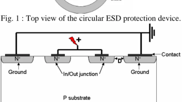
In this study, the Devices Under Test (DUT) are “circular” bidirectional diodes used as ESD protection devices. They consist of two back-to-back diodes arranged in a cylindrical symmetry (Fig. 1 and Fig. 2).
Fig. 1 : Top view of the circular ESD protection device.
Fig. 2 : Circular ESD protection ESD cross section. The circular diodes have been processed on the same P substrate, whereas In/Out and ground junctions have the same N+ doping (Fig. 2). In this device, the P substrate is not connected.
IC technology developments aim at smaller devices, which represent a real challenge since several authors have shown that shrinking structure dimensions drastically reduces ESD robustness performances [2]. In this study, the distance D between the In/Out junction and the ground one has been varied to investigate the impact of this parameter on the ESD failure mechanisms. Hence, the following distances have been designed: 35µm, 45µ m, 55µ m and 65µ m.
The ESD stresses applied to the DUT of this study follow the IEC 61000-4-2 norm conditions for an Electromagnetic Compatibility [2], which is intended to simulate a person discharging into a system while holding a metal object [3]. Touching with a metal object suggests that, at least for the early part of the discharge, there will be a small resistance in the discharge path in addition to the arc resistance then leading to a very high current peak. When the air breaks down between the metal and one pin of the Integrated Circuit (IC), the protection structure turns on and the capacitance of the person is discharged via the IC into ground.
The IEC 61000-4-2 waveform produced by our ESD tester is represented in Fig. 3.
0 200 400 600 800 1000 1200 1400 1600 0 10 20 30 40 50 60 70 80 90 100 110 Time (ns) C u rr e n t 99% Ipeak Ipeak tr
Fig. 3 : IEC 61000-4-2 contact waveform from NoiseKens ESS2000 ESD tester.
NoiseKens ESS-2000AX is the ESD simulator that allows applying single and repetitive IEC61000-4-2 pulses on protection diodes with a 1Hz frequency. All tests in this work are realized in contact discharge mode.
During electrical or ESD tests, protection diodes are connected and polarized as shown in Fig. 2.
a. Standard ESD testing results
Three positive pulses followed by three negative ones have been applied to the devices to evaluate the single-ESD-robustness level (VESD). This robustness
testing procedure corresponds to the standard qualification method as opposed to the repetitive pulse method presented in the next section. The single-ESD-robustness level is defined as the minimum stress level applied in successive three zaps which induces any change in the I(V) initial characteristic.
In the following test results, the applied stress voltage begins at 5kV stepping up by 0.5kV. Therefore, VESD have been defined as the minimum stress voltage
after which any reduction of the breakdown voltage or any increase of the leakage current is observed in the protection device I(V) characteristic compared to the initial electrical measurement.
Ten devices have been studied for each distance D and the average VESD is summarized in Fig. 4. It can be
noticed that VESD slightly improves with the distance D.
10 10.5 11 11.5 12 30 35 40 45 50 55 60 65 70 Distance (µm) V E S D ( k V )
Fig. 4 : ESD Robustness for a single pulse as a function of distance D.
Considering the number of tested samples, a tight distribution can be noticed in the robustness for a fixed distance. In fact, 10.5kV < VESD < 11.5kV for all
distances.Since, the minimum level robustness is equal to 10.5kV; an investigation on repetitive ESD behavior can be done at 10kV, which is always sustained by all back -to-back diodes samples.
b. Repetitive pulses results
The repetitive pulse testing method significantly differs from the standard one and could be defined as a new qualification procedure. The aim of the repetitive pulses study is to determine the number of pulses, noted
Nbd, after which the diode is damaged with a given
stress level applied in a repetitive way. Practically, the ESD voltage level is repeated with a pulse rate of one pulse per second. The voltage polarity is always positive at the in/out junction, since by device geometry, the negative robustness exceeds NoiseKens tester stress capability (30kV).
The same strict degradation criterion is defined as any I(V) characteristics change like in the single pulse case. The ESD robustness for repetitive stress corresponds now to the number of pulses sustained by the protection device just before electrical failure at a given stress voltage.
In Fig. 5 the repetitive robustness results are shown for 10kV and 10.5kV IEC voltages.
The measurements data of Fig. 5 have been obtained after a statistical treatment from 17 protection devices robustness measurements for each different distance value. Weibull statistical distribution has been exploited to take into account that some samples are not degraded by 1000 ESD zaps in order to analyze the number of pulses leading to failure. In fact, the description of statistics using Weibull distribution, which is a distribution in ln(x), is appropriate for a statistic study of reliability data. The improved repetitive stress robustness with the distance D has been globally shown in spite of robustness dispersion. Therefore, these results confirm that shrinking these protection device sizes reduces the ESD robustness of
protection components, both for single and repetitive stresses. 0 100 200 300 400 500 600 700 800 900 1000 1100 1200 35 40 45 50 55 60 65 70 Distance (µm) N b d ( p u ls e s ) 10 kV 10.5 kV
Fig. 5 : ESD robustness for 10kV and 10.5kV repetitive pulses as a function of distance D.
0 2 4 6 8 10 12 14 16 18 20 10 15 20 25 30 35 40 45 VTLP (V) IT L P ( A ) 35µm surrounded 45µm surrounded 55µm surrrounded 65µm surrounded
Fig. 6 : Quasi-static TLP characteristic (100ns pulsed measurement) of studied protection devices showing on resistance increasing with D.
It is very interesting to consider the impact of the above results on the usual way of designing ESD protection strategy. Given the increase of the on-resistance RON with distance D (Fig. 6) and the single
pulse robustness (Fig. 4), the ESD engineer may choose the lowest distance D device to protect a circuit that could for example sustain a maximum voltage of 45V. He may consider the RON benefit being more important
than the slight increase in ESD robustness. But this selection is in fact sub-optimal regarding repetitive ESD robustness. Indeed, for application in the field, the product designed using the device with shorter distance D will only survive to about 40 stresses at 10kV while the protection device with longest distance D would survive more than thousands ESD stresses at the same level (Fig. 5)
Comparing the behaviour of single and repetitive robustness versus distance D (Fig. 4 and Fig. 5), we could assume distinct failures mechanisms. In fact, the ESD robustness level voltage in the standard test is apparently higher than in repetitive mode. However, given the number of single pulsed samples, this statistically does not allow concluding strictly on that observation.
To investigate further the failure mechanisms occurring during repetitive ESD stress, it is interesting
to proceed to the physical characterization of degraded diodes.
4. Physical failure analysis
The objectives of this physical analysis is firstly to localize the failure, and then to determine the defect nature. Here, results are shown for protection devices degraded by repetitive 10kV IEC pulses. Several methods such as OBIRCH (Optical Beam Induced Resistance Change), EMMI (EMission MIcroscope) have been exploited without success because defects illumination is covered by the metal layer and the leakage current demanded to detect failures is high compare to the back-back leakage current.
A chemical decoration method called “Sirtl etch” allowed revealing the failures. Fig. 7 shows melted filaments generated in the silicon bulk by repetitive ESD stresses.
(a) (b)
(c) (d)
(e) (f)
Fig. 7 : Failure analysis on 35µ m (a) & (b), 45µ m (c) & (d) and 55µ m (e) & (f) circular ESD protection diodes degraded by 10.5kV repetitive ESD stresses.
After a complete removal of the metallization, the Sirtl etch procedure enables to expose the silicon bulk. Failure locations are then visualized with a Scanning Electron Microscope (SEM) and they clearly correspond to buried melted point not visible before chemical decoration. For all distances, from 35µ m to 65µ m, failures are localized at the periphery of the
In/Out junctions. A zoom of melted filament in Fig. 7 also allows distinguishing around the melted filament, triangular defaults suspected to be dislocations [4].
The observed ESD failure signature is apparently always related to a single melted filament. So, to thoroughly examine the evolution of these ESD defects during pulses repetitions, electrical characterization have been carried out.
5. Electrical Characterization
The typical I(V) characteristic evolution observed for a protection device degraded by repetitive 10kV stresses is presented in Fig. 8 for D=45µ m. A similar evolution of the electrical degradations is obtained for protection devices studied from D=35µ m to 65µ m, only the number of pulses before degradation (Nbd) differs.
0.E+00 2.E-07 4.E-07 6.E-07 8.E-07 0 2 4 6 8 10 12 14 16 18 Voltage (Volts) L e a k a g e C u rr e n t (A ) 75 pulses 80pulses 85pulses 100pulses 130pulses 1.E-10 1.E-09 1.E-08 1.E-07 1.E-06 1.E-05 1.E-04 0 2 4 6 8 10 12 14 16 18 Voltage (Volts) L e a k a g e C u rr e n t (A ) 75 pulses 80pulses 85pulses 100pulses 130pulses
Fig. 8 : Electrical evolution of latent defects with a linear (a) and logarithmic (b) scalar for 45µ m circular diode degraded in Fig. 7 (c) & (d).
The I(V) evolution presented in Fig. 8 has been obtained by recording the static electrical behaviour of the diode after applying ESD stresses by steps of five repetitive pulses. Considering the strict repetitive device degradation criterion defined in section 3.a., the device has been degraded after 80 zaps. Indeed, linear and logarithmic curves in Fig. 8 show clearly that both the breakdown voltage and the leakage current evolution remain unchanged before the first 75 pulses.
Two hypotheses may be considered to explain failure mechanism. In the one hand, no defect is created in the structure up to a random occurrence of a current filament in the silicon creating a local defect. In the
other hand, the ESD degradation could be based on a defect created during the 75 first pulses but not revealed electrically [5]. At this point in time, experimental results do not allow favouring one of these two hypotheses.
The step-stress after the 75 pulses leads to a progressive degradation that seems to reveal a growing defect density creation with additional stresses. An ultimate degradation state is completely reached when the I(V) characteristic becomes almost unchanged after 130 pulses. Therefore, the defect is established and result on an irreversible failure.
As described in section 4, these failures have been visualized from physical analysis. Their localization is always found to be in the periphery of the In/Out junction. By correlating the physical analysis results to the electrical ones, we can propose a final degradation scenario based on the growing of the original defects size in the periphery of the In/Out junction, leading finally to a short circuited junction once a critical defect size has been reached.
7. Conclusion
This article describes, through physical and electrical characterizations, the failure mechanisms of discrete ESD protection devices subjected to repetitive ESD pulses. Electrical degradation behaviour and melted filaments appearing in the silicon bulk revealed that ESD defects appear and grow during pulses repetition. Repetitive ESD testing allows to drawn new and original conclusions for protection design. Furthermore an approach of defect evolution has been established in this article. Unfortunately, the ESD defect nature is not physically visible. Nevertheless, investigations continue through innovation of new protection diodes design for sustaining repetitive 15kV IEC pulses and improving the understanding of the real defect nature and origin.
References
[1] A. Amerasekara, C. Duvvury, “The Impact Technology Scaling on ESD Robustness and Protection Circuit Design” EOS/ESD Symposium, EOS-16, 1994, page 237-245.
[2] Electromagnetic Compatibility (EMC) Part 4-2, “Testing and Measurement Techniques -Electrostatic discharge immunity test”, IEC 61000-4-2 Ed 1.2 2001-04.
[3] R. Ashton, “The future of ESD testing” Conformity, Dec. 2008, P. 14-21
[4] C. Hashimoto, K. Okuyama, K. Kubota and H. Ishizuka, « Degradation of I/O devices due to ESD-Induced Dislocations », IEEE Trans. On Electron Devices, 1994
[5] F. Essely, C. Bestory, N. Guitard, M. Bafleur, A. Wisley, E. Doche P. Perdu, A. Touboul, D. Lewis “Study of ESD defects impact on ICs reliability”, Micro. Reliability 44 (2004) P. 1811-1815
(a)