Characterization and Requirements for Cu-Cu Bonds
for Three-Dimensional Integrated Circuits
by
Rajappa Tadepalli
B.Tech., Indian Institute of Technology - Madras, India (2000)
S.M., Massachusetts Institute of Technology (2002)
Submitted to the Department of Materials Science and Engineering
in partial fulfillment of the requirements for the degree of
Doctor of Philosophy
at the
MASSACHUSETTS INSTITUTE OF TECHNOLOGY
February 2007
© Massachusetts Institute of Technology 2007. All rights reserved.
Author ...
Department of Materials Science and Engineering
6 November 2006
Certified by ...
Carl V. Thompson
Stavros Salapatas Professor of Materials Science and Engineering
Thesis
Supervisor
Accepted by ...
Samuel
M.
Allen
POSCO Professor of Physical Metallurgy
Characterization and Requirements for Cu-Cu Bonds
for Three-Dimensional Integrated Circuits
by
Rajappa Tadepalli
Submitted to the Department of Materials Science and Engineering on 6 November 2006, in partial fulfillment of the
requirements for the degree of Doctor of Philosophy Abstract
Three-dimensional integrated circuit (3D IC) technology enables heterogeneous integration of devices fabricated from different technologies, and reduces global RC delay by increasing the device density per unit chip area. Wafer-level Cu-Cu thermocompression bonding provides an attractive route to 3D IC fabrication, with Cu serving as both the electrical and mechanical interconnection between adjacent device layers. While the bonding process is currently employed for such applications, the lack of quantitative understanding of the bond quality and reliability has made developing robust processes extremely challenging. The current work addresses this problem through the development and implementation of bond toughness measurement techniques that investigate the effects of thin film patterning, surface chemistry and process parameters on the Cu-Cu bond quality under a range of loading conditions.
The four-point bend test was used to quantify Cu-Cu bond toughness, Gc, under
mixed-mode loading and to develop an optimized process flow that enabled the creation of high- toughness bonds (> 5 J/m2) at a bonding temperature of 300 oC. Mixed-mode loading induces significant plastic energy dissipation in ductile layers, resulting in an overestimation of the true adhesive strength of the interface. The chevron test method has been developed to allow bond toughness measurements under mode I loading, thereby probing the ‘true’ work of adhesion of the bonded interface. Furthermore, analysis of the bonded chevron specimen with different layer thicknesses was performed to allow the specimen to be used to characterize the bonded interface under mixed-mode loading conditions. Chevron tests reveal that the toughness of patterned Cu films is a strong function of the feature size and orientation. For debond propagation across periodic bonded and unbonded regions, a pronounced increase in Gc was observed, compared to
debond propagation along a continuous bonded interface. Effects of patterning were significantly different in ductile thermocompression and brittle fusion bonded systems, with the latter showing a reduction in toughness due to patterning.
The ultimate limit of low temperature Cu-Cu adhesion was investigated using pull-off force measurements in Atomic Force Microscope (AFM) under ultra-high vacuum (UHV) conditions. These measurements show that the work of adhesion of Cu bonds created at room temperature is ~ 3 J/m2, similar to Gc for wafer-level bonds created at 300 oC and measured
using the chevron test. Deliberate pre-adhesion exposure of the Cu surfaces to 10-6 Torr O 2 leads
to a dramatic reduction in adhesion (to 0.1 J/m2), suggesting the formation of a Cu oxide that is
detrimental to the Cu bonding process. The UHV-AFM measurements suggest that strong Cu-Cu bonds can be created by bonding clean Cu-Cu surfaces at room temperature, thereby eliminating several thermal stability issues in the thermocompression bonding process.
The thermal management problem in 3D ICs containing multiple device layers was examined using an analytical model of forced liquid cooling via Cu-sealed integrated microchannels. Integration of microchannels requires a reduction in the area available for interconnects and adhesion, causing a trade-off between the inter-layer bonded area and the size and density of the channels that can be included. The optimum channel density is a function of the achievable local Cu-Cu bond strength.
Thesis Supervisor: Carl V. Thompson
Acknowledgements
First and foremost, I am grateful to God Almighty for blessing me with the strength and energy to pursue my dreams. Without His grace, none of this work would have been possible.
During my stint at MIT, I had the privilege of working with some brilliant minds. I would first like to thank my thesis advisor, Professor Carl Thompson, for accepting this novice researcher in his group six years ago and for providing me with all the tools and the intellectual freedom to pursue the projects of my interest. Essentially, Carl taught me how to perform research. Above all, I will always remember Carl for his passion for all things science, and for his sincere and ethical approach towards research. Several other faculty members at MIT have contributed to my thesis work. In particular, I am grateful to my thesis committee members, Prof. Samuel Allen and Prof. Duane Boning, for the stimulating discussions and their valuable comments on the dissertation. I am also indebted to Prof. Donald Troxel and Prof. Rafael Reif, who have provided several key inputs to this project as part of the MIT 3D IC team.
I acknowledge the contributions from all my collaborators, especially Prof. Kevin Turner, who has been a constant source of information on fracture mechanics and mechanical testing. Some of the key results in this thesis have been a result of our joint efforts. I am also grateful to Ajay Somani and Prof. Duane Boning for collaborating on the fusion bonding work, which has added a useful new dimension to my research. I am appreciative of the discussions by Prof. Chee Lip Gan and Leong Hoi Liong of NTU-Singapore during our numerous early morning (and late night in NTU-Singapore!) meetings. I wish to thank Dr. Andy Fan, Dr. Ramkumar Krishnan, Dr. Syed Alam, Dr. Chuan Seng Tan and Dr. Christine Tsau for the various brainstorming discussions that have helped shape this project.
Several research staffs have helped me with my experiments over the course of this work. I am indebted to Kurt Broderick for educating me on microfabrication and cleanroom operation. I also acknowledge the help from
all the other MTL and CMSE staffs and students. I am grateful to Dr. Richard Schalek of Harvard University for all the long hours and the useful discussions on the UHV-AFM project.
I am thankful to the CVT group members, with whom I have shared many scientific and philosophical conversations over the years. In particular, I will fondly remember the association with Ramkumar Krishnan, Harsh Verma, Zung-Sun Choi, Reiner Mönig, Robert Bernstein, Cody Friesen, Amanda Giermann, Frank Wei, Jihun Oh and Jeff Leib. I count myself lucky to have made several friendships during my stay at MIT, which will hopefully be life long. Though numerous to list, I would like to thank Chaitanya Ullal, Ramkumar Krishnan, Ajay Somani, Harsh Verma, Sajan Saini, Ramachandran Balakrishna and Srinivasan Sundaram for their support during some testing periods in my graduate student life.
Mere words do not suffice to express my gratitude to my family that has been chiefly responsible for whatever little I have achieved. My parents, Late Shri. Gopalakrishna and Smt. Vijayalakshmi have toiled and sacrificed a lot in their lives to provide the best education for my brother and myself. This dissertation is just a small token of gratitude for their efforts. My only regret is that my father is not alive to witness this moment. I am indebted to my brother Hari for being there for me whenever it counts. My better half, Padmashree, has been my best friend and the strongest source of support throughout my graduate years. Despite all the hurdles that we faced, Padma has been with me all the way. Moreover, she has shelved many of her ambitions to help me pursue this work. More than anything, Padma has given me the greatest gift of all, our baby Aniket, whose mere presence fills our lives with so much joy. I can only hope that over this lifetime, I can return the love that Padma has given me.
Contents
1 Introduction
17
1.1 Vertical Integration of Integrated Circuits……….. 17
1.2 Motivation – Challenges in 3D IC Technology………. 19
1.2.1 Wafer Bonding Characterization………... 19
1.2.2 Thermal Management ………... 23
1.3 Thesis Objectives………... 23
1.4 Thesis Scope………... 24
2
Wafer Bonding Characterization – Background and Motivation 27
2.1 Three-Dimensional Integrated Circuits... 27
2.1.1 Interconnect Wire Length Reduction with 3D ICs... 28
2.1.2 System-on-Chip Design... 29
2.1.3 Thermal Performance of 3D ICs... 30
2.1.4 Fabrication Schemes for 3D ICs... 32
2.2 Wafer Bonding... 35
2.3 Copper Thermocompression Bonding... 38
2.4 Bond Toughness/Interface Adhesion... 42
2.4.1 Measurement of Interface Adhesion... 43
2.4.2 Application of Fracture Mechanics to Interface Adhesion... 44
2.5 Bond Toughness Measurement Methods... 48
2.6 Summary... 57
3
Four-Point Bend Testing of Wafer-level Cu-Cu Bonds –
Effects of Temperature and Surface Preparation
58
3.1 Experimental Procedure... 58
3.1.1 Test Structure Fabrication... 58
3.1.2 Four-Point Bend Test... 63
3.2 Results... 65
3.2.1 Toughness of Bonded Continuous Films... 66
3.2.2 Toughness of Bonded Lines... 66
3.3 Discussion... 71
4
Chevron Testing of Wafer-level Bonds –
Modeling and Mixed-mode Analysis
74
4.1 Chevron Test Specimen... 74
4.2 Chevron Test... 75
4.3 Chevron Specimen Modeling... 77
4.3.1 Finite Element Model... 77
4.3.2 Calculation of Strain Energy Release Rate and Phase Angle... 78
4.4 Results... 79
4.5 Discussion... 84
4.6 Summary... 85
5
Mode I Chevron Testing of Wafer-level Cu-Cu Bonds –
Process Parameter Studies
86
5.1 Experimental Procedure... 86
5.1.1 Test Structure Fabrication... 86
5.1.2 Chevron Test... 91 5.2 Results... 92 5.2.1 Mode I Toughness... 93 5.2.2 Process Optimization... 94 5.3 Discussion... 99 5.4 Summary... 102
6
Mixed-mode Toughness of Cu-Cu Bonds Using Asymmetric
Chevron
Test
103
6.1 Experimental Procedure... 103 6.2 Results... 104 6.2.1 Mixed-mode Toughness... 104 6.2.2 Failure Loci... 106 6.3 Discussion... 110 6.4 Summary... 1117
Interface Toughness of Patterned Cu-Cu Bonds
112
7.2 Results... 116
7.2.1 Mode I Bond Toughness vs. Pattern Size... 116
7.2.2 Mixed-mode Bond Toughness vs. Line Width... 118
7.2.3 Failure Loci... 119
7.3 Discussion... 123
7.4 Summary... 128
8
Interface Toughness of Patterned SiO
2Fusion Bonds
129
8.1 Experimental Procedure... 130
8.2 Results... 131
8.3 Discussion... 133
8.4 Summary... 135
9
Low-Temperature Cu-Cu Adhesion Measurements in UHV-AFM 137
9.1 Experimental Procedure... 137 9.1.1 Sample Preparation... 137 9.1.2 Force Measurements... 138 9.2 Results... 141 9.3 Discussion... 143 9.4 Summary... 147
10
Optimized Design of Bonded Microchannels
148
10.1 Microchannel Cooling Model... 148
10.2 Results... 151
10.3 Discussion... 156
10.4 Summary... 159
11
Conclusions and Recommendations
161
11.1 Summary and Discussion... 161
11.2 Conclusions... 165
11.3 Recommendations for Future Work... 166
A.1 MIT 3-D Process... 168
A.2 Four-Point Bend Test Specimen Fabrication... 169
A.3 Chevron Test Specimen Fabrication... 171
B
Fabrication and Strength Testing of Bonded Microchannels
173
B.1 Microchannel Fabrication... 173
B.2 Microchannel Pressurization... 175
B.3 Microchannel Bond Toughness – Chevron Test... 176
B.4 Summary... 177
C
Chevron Model Finite Element Code
178
List of Figures
1-1 Schematic of 2-layer 3D IC... 18
1-2 Schematic cross-sections of 3D ICs created by metallic and dielectric bonding schemes... 20
1-3 Schematic of loading conditions of a bonded interface... 22
2-1 Wire-length distribution in 2D and 3D ICs... 28
2-2 Schematic of 4-layer 3D IC... 29
2-3 Chip temperature rise in 2D and 3D ICs... 30
2-4 Schematic of 3D IC with integrated microchannels... 31
2-5 Schematic illustration of fracture toughness vs. phase angle... 46
2-6 Schematic illustration of bond strength testing methods... 49
2-7 Schematic of four-point bend test specimen... 52
2-8 Schematic of chevron bond test... 55
3-1 EV501TM wafer bonding setup... 62
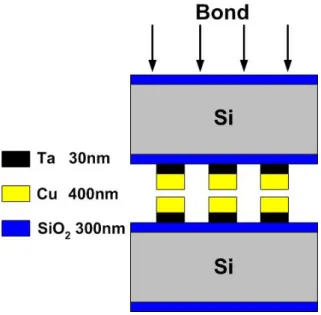
3-2 Schematic cross-section of bonded patterned lines for four-point bend tests... 62
3-3 IR picture of bonded wafer with four-point bend test specimens... 63
3-4 Schematic of four-point bend test alignment fixture... 65
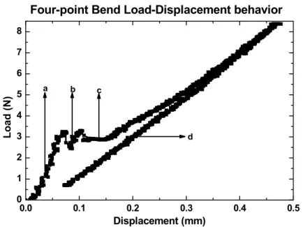
3-5 Load-displacement behavior from four-point bend test... 67
3-6 Cu-Cu bond toughness vs. bonding temperature and surface preparation measured using four-point bend test... 68
3-7 SEM micrographs of four-point bend test fractured surfaces... 71
4-1 Schematic of chevron test specimen... 76
4-2 Load-displacement behavior from chevron test... 77
4-3 Finite element mesh for chevron model... 78
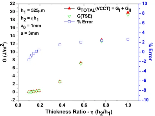
4-4 VCCT vs. TSE comparison for strain energy release rate computation... 80
4-5 Phase angle vs. layer thickness ratio, predicted by chevron FE model... 81
4-6 Chevron geometry function vs. crack length ratio... 82
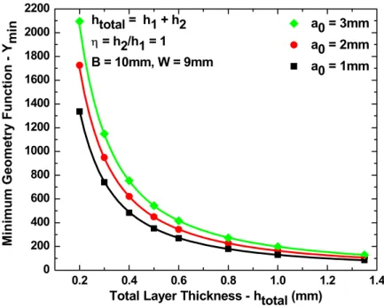
4-7 Minimum geometry function vs. total layer thickness... 83
4-8 Minimum geometry function vs. layer thickness ratio... 83
5-1 Mask layout of chevron structures and lines... 87
5-2 Schematic of wafer bow configurations... 89
5-4 Load-displacement behavior from chevron test... 92
5-5 AFM images of fractured surfaces (effect of pre-bond clean)... 95
5-6 SEM micrographs of fractured surfaces (effect of pre-bond clean)... 95
5-7 Pure mode I Cu-Cu bond toughness vs. wafer bow... 96
5-8 AFM images of ECP and e-beam evaporated Cu films prior to bonding... 98
5-9 SEM micrographs of fractured surfaces of ECP and e-beam evaporated bonded Cu films... 99
6-1 Schematic of mode I and mixed-mode bonded chevron specimens... 104
6-2 Cu-Cu bond toughness vs. phase angle measured by chevron test... 105
6-3 Schematic of failure modes in bonded Cu specimens... 107
6-4 SEM micrographs of mixed-mode fractured surfaces... 108
6-5 AFM images of mixed-mode fractured surfaces... 109
7-1 Schematic description of continuous and discontinuous bonded interfaces.... 112
7-2 Mask layouts of patterned line and pad structures... 113
7-3 Schematic illustration of chevron specimens with bonded lines and pads... 115
7-4 Mode I Cu-Cu bond toughness vs. line width for orthogonal and parallel lines.116 7-5 Mode I Cu-Cu bond toughness vs. pad size... 117
7-6 Mode I Cu-Cu bond toughness vs. feature size (lines and pads)... 117
7-7 Mixed-mode Cu-Cu bond toughness vs. line width for orthogonal and parallel lines... 118
7-8 Cu-Cu bond toughness vs. phase angle for orthogonal and parallel lines... 119
7-9 Fractured surfaces of bonded orthogonal lines (mode I and mixed-mode)... 120
7-10 Fractured surfaces of bonded pads... 122
7-11 Toughness of bonded Cu-Cu orthogonal lines and pads vs. number of crack nucleation events... 124
7-12 Schematic depiction of crack front area in bonded orthogonal lines and pads. 124 7-13 Toughness of bonded Cu-Cu orthogonal lines and pads vs. number of crack nucleation events and crack front area... 126
8-1 Schematic cross-section of a SiO2 fusion bonded chevron specimen... 130
8-2 SiO2 fusion bond toughness vs. pattern size... 131
8-3 SEM micrographs of SiO2 fusion bond fractured surfaces... 132
8-4 SiO2 fusion bond toughness vs. perimeter per unit bonded area... 134
9-1 AFM force-distance curve... 140 9-2 Schematic of AFM force-distance curve showing
cantilever tip - substrate interaction... 140
9-3 STM images of UHV- deposited Cu films... 141
9-4 SEM micrographs of Cu-coated AFM cantilever tips... 142
9-5 Room temperature Cu-Cu work of adhesion vs. applied load... 142
9-6 Work of adhesion of clean and oxidized Cu surfaces as a function of temperature... 143
9-7 Cu-Cu work of adhesion vs. applied load showing plasticity contribution... 144
10-1 Schematic of microchannels in back-to-back bonded layers... 149
10-2 Equivalent microchannel cooling scheme... 149
10-3 Microchannel thermal resistance vs. channel width... 152
10-4 Microchannel thermal resistance and Reynolds number vs. channel width.... 153
10-5 Minimum thermal resistance as a function of fin-channel width ratio... 153
10-6 Chip temperature rise vs. bonded area fraction... 154
10-7 Chip temperature rise vs. channel depth... 155
10-8 Coolant pumping power vs. fin-channel width ratio... 156
10-9 Chip temperature rise and macroscopic bond strength vs. bonded area fraction... 157
10-10 Chip temperature rise vs. local bond strength... 158
A-1 MIT 3-D process flow... 168
A-2 Four-point bend test specimen fabrication process flow... 169
A-3 Chevron test specimen fabrication process flow... 171
B-1 Schematic cross-section of bonded microchannels... 174
B-2 SEM micrographs of cross-section of bonded channels... 174
B-3 SEM micrographs of cross-section of bonded channels after pressurization.. 175
B-4 SEM micrographs of cross-section of bonded chevron specimens containing channels... 176
List of Tables
3-1 Cu-Cu bond toughness vs. stack thickness from four-point bend tests... 70
5-1 Silicon Nitride deposition parameters for inducing wafer bow... 89
5-2 Effect of pre-bonding clean on mode I Cu-Cu bond toughness... 94
5-3 Pure mode I Cu-Cu bond toughness vs. Cu deposition process... 97
6-1 Si wafer thicknesses for chevron mixed-mode experiments...103
6-2 Variation of the failure loci with mode-mixity in Cu-Cu bonds measured using chevron test... 107
6-3 Estimated plastic zone sizes as a function of phase angle for Cu-Cu bonds under mixed-mode loading... 110
7-1 Description of mask layouts of patterned line and pad structures... 114
9-1 Diffusion coefficients and diffusion lengths of Cu at different temperatures... 146
11-1 Summary of patterning effects in ductile (thermocompression) and brittle (fusion) bonded systems... 164
B-1 Mode I toughness of bonded microchannels and lines measured using chevron test... 177
Chapter 1
Introduction
1.1 Vertical Integration of Integrated Circuits
The innovation of the planar transistor in 1959 is viewed as the origin of “Moore’s Law”, by Gordon Moore himself [Scha, 1996]. Moore’s Law, which states that the number of transistors on a chip doubles about every two years, has become a barometer for rapid technological change. For over four decades, Moore’s Law has been sustained, and therefore, higher computing performance has been achieved, primarily through rigorous scaling of transistor device dimensions. As the technology approaches atomic dimensions, a fundamental barrier to scaling is on the horizon. Solutions beyond Silicon CMOS technology, based on molecular electronics will revolutionize computation in future by scaling into the third dimension. However, in the more immediate future, device scaling can be sustained by the extension of standard silicon processes into the vertical dimension in the form of Three-Dimensional Integrated Circuits (3D ICs).
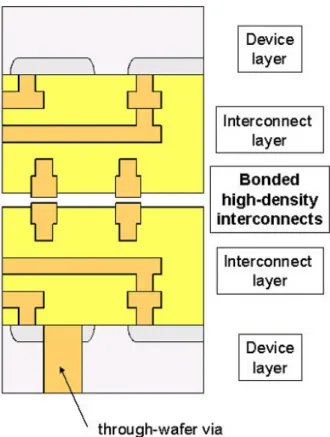
3D IC technology enables the vertical integration of a stack of device layers (with their associated metallization levels, i.e. interconnects) using inter-layer interconnections for electrical and mechanical connectivity (Fig. 1-1). In traditional 2D ICs, the device dimensions continue to shrink and the interconnect pitch continues to decrease to meet the wiring density requirement. This reduction in pitch, coupled with smaller wire cross-sections and longer lines, increases the RC delay or global interconnect latency [Sara, 1992]. Owing to the vertical construction, three-dimensional ICs are expected to reduce the semi-global and global wiring requirements significantly, therefore, allowing higher packing density in wiring-limited ICs and smaller interconnect delay [Rahm, 2000].
In general, there are two primary fabrication schemes for wafer-scale integration of integrated circuits. One option is to sequentially form a stack of active device layers (“bottom-up” approach). Another route is parallel assembly of the finished device layer (“assembly” method).
In the bottom-up approach, devices in each active layer are processed sequentially starting from the bottom-most layer. Devices are built on a substrate wafer by mainstream process technology. After proper isolation, a second device layer is formed and devices are processed by conventional means on the second layer is
Fig. 1-1. Schematic of a 3D IC consisting of two device levels and their associated interconnect levels. The device layers are bonded with high density interconnects. [Figure provided by C. V. Thompson]
formed and devices are processed by conventional means on the second layer. This sequence of isolation, layer formation, and device processing can be repeated to build a multi-layer structure. This bottom-up approach has the advantage that precision alignment between layers can be accomplished. However, it suffers from a number of drawbacks. The crystallinity of upper layers is usually low and imperfect. As a result, high-performance devices cannot be built in the upper layers. Thermal cycling during upper-layer crystallization and device processing can degrade underlying devices and therefore a tight thermal budget must be imposed. Due to the sequential nature of this method, manufacturing throughput is also low.
The “assembly” method, on the other hand, allows one to fabricate individual 2D circuits using conventional planar fabrication technology; these 2D circuits can then be tested and assembled to form 3D circuits. While it is possible to stack high-performance devices, this method poses new challenges. Precision alignment between layers can impose a limit on the density of vertical interconnects. Low-temperature layer transfer techniques are also needed, and recent progress in wafer bonding has been
encouraging [Pete, 2003]. Since device layers can be fabricated in parallel and optimized using their respective technologies prior to layer stacking, higher throughput can be expected. This feature also enables heterogeneous integration of materials and functionalities, i.e. System-on-a-Chip (SoC).
1.2 Motivation - Challenges in 3D IC Technology
The successful implementation of 3D IC technology hinges on the development of a robust process flow and addressing potential thermal/mechanical reliability issues during device operation. The key technological challenges in 3D IC development are:
• Process development related to alignment and bonding of multi-layer stacks. • Heat dissipation through a stack of Si wafers separated by dielectric materials
that have poor thermal conductivity.
1.2.1 Wafer Bonding Characterization
Wafer bonding has emerged as an important tool in the fabrication of a range of microsystems technologies, including advanced integrated circuits [Fan, 1999], microelectromechanical systems (MEMS) [Schm, 1998], and the manufacture of silicon-on-insulator (SOI) substrates [Cell, 2003]. Typically, wafer bonding processes involve joining substrates of 100 mm - 300 mm diameter and 0.5 mm - 1.0 mm thickness. The common bonding mechanisms are, a) direct bonding, where flat and smooth surfaces are brought into contact at room temperature followed by annealing at high temperatures [Plöß, 1999], b) anodic bonding, which uses an electrostatic field in combination with high temperatures [Coz, 1995], c) thermocompression bonding, where intermediate metallic/polymer layers are used to form a bond under applied temperature and pressure [Fan, 1999], [Eat, 1994], and d) solder/eutectic bonding, where a bond is formed by the melting and solidification of an alloy material [Til, 2000].
Wafer bonding schemes for 3D ICs can be classified into “via-last” and “via-first” approaches. When the bonding medium between active layers is insulating, a “via-last” sequence is followed. Device layers are first bonded and vertical vias are etched through the bonding interface. Therefore, high-aspect-ratio vertical vias are needed. Examples of such bonding media include polyimide adhesive, polymeric adhesive, and silicon oxide. Device layers can also be bonded with a conductive metallic layer, which allows for a “via-first” approach for fabricating 3D ICs. When metal is used as the bonding medium,
vias can be formed in both paired device layers prior to bonding, hence the requirement for interlayer via aspect ratio can be relaxed. For the case of metal bonding, the bonded inter-wafer connections do not consume active device area, enabling a significantly higher signal bandwidth between device layers. However, in many integration schemes, through-wafer vias are still needed for power, input/output (I/O), and signal routing through the device strata, as well as for inter-wafer connections for multi-strata stacking. Although these through-wafer vias will consume some active device area, overall, metal bonding still provides a significant bandwidth advantage over dielectric bonding. The inter-wafer bandwidth is an important parameter for applications such as 3-D logic in microprocessors where the die-to-die via pitch requirements can be extremely tight [Blac, 2004]. Figure 1-2 shows the schematic cross-sections of 3D ICs created by metallic and dielectric (SiO2) bonds. The bonding plane of the metallic bonds is used for
interconnections, whereas through-wafer vias are required for dielectric bonds.
(b) (a)
Fig. 1-2. Schematic cross-sections of 3D ICs created by a) Metallic bonds [Morr, 2006] and b) Dielectric (SiO2) bonds [Koob, 2005]. For metallic bonding, the bonded interconnects do not
consume active device area, whereas vertical vias are required for dielectric bonding schemes.
In this work, the Cu thermocompression bonding process is studied as a means to achieve a permanent bond to hold active device layers together in a multi-layer stack. Metallic Cu wafer bonding is an attractive choice because the same bonding medium acts as an electrical bond to establish a conductive path between active layers in a 3D IC, and also as a mechanical bond to hold the active layers together reliably. In Cu wafer bonding, the bond is created by the application of temperature (300 oC – 400 oC) and
pressure to bring two wafers with Cu layers together. Several facets of Cu wafer bonding technology have to be addressed to enable development of a robust process flow:
Ultra-low-temperature bonding (< 100 oC)
Since device wafers that have completed front-end and some back-end steps are bonded to each other, low-temperature bonding is highly desired. This is essential to prevent damage to the devices and to be compatible with low-κ dielectrics. Low temperature bonding is also important to reduce stresses due to thermal mismatch of different materials.
Creation of high-density interconnections between device layers depends on the ability to align features with a very fine pitch. The smallest feature size on the bonding plane, and therefore, the packing density of interconnects, is being dictated by the limits of wafer-to-wafer alignment. Alignment is affected by thermal strain during the thermocompression bonding process. Therefore, ultra-low-temperature bonding has the potential to minimize or eliminate wafer-to-wafer (or die-to-die) misalignment.
Bond characterization and reliability
The concern for mechanical reliability exists in present day 2D ICs containing millions of transistors on a microprocessor chip, where the interconnect layers are densely stacked to form the multi-layer interconnect structure. In such a structure, the interconnect lines and the vias are embedded in a matrix of the ILD. Due to the large difference in thermal expansion coefficient between the metal, barrier layer and the surrounding ILD, tensile stresses generated in the interconnect lines are large enough to make the interfaces vulnerable to fracture failure. Interface decohesion is bound to be a much more potent problem when a switch is made from 2D to 3D ICs. In 3D ICs fabricated using wafer bonding technology, not only are more interfaces present compared to 2D ICs, but there also exists the crucial bonded interface. Determination of the mechanical strength of the bonded interface is an essential requirement in developing wafer bonding processes. Bonded interfaces are subjected to thermal/mechanical stresses during both fabrication and device operation. Quantitative characterization of bond strength is critical for developing processes that enable the fabrication of devices with long-term reliability. Though work has been done towards measurement of adhesion properties of multi-layer thin film structures, the bond quality and reliability of Cu-Cu bonds for 3D applications have not been studied in quantitative detail.
A critical requirement for bond toughness measurements is that the test mimics the real case. Hence, the type of load that the bond is subjected to in the resulting
device should, to a great extent, determine the choice of method. If the bonded structure is to be subjected to tensile forces, then a tensile test method may be preferable. Common loading conditions are tension (mode I), shear (mode II), and mixed-mode (mode I + mode II), as shown in Fig. 1-3. Since 3D ICs and other devices created by wafer bonding are subjected to different loading conditions during fabrication and operation, bond toughness values have to be evaluated under different mode-mixities.
a) b) c)
Fig. 1-3. Loading conditions of a bonded interface. a) mode-I (pure tension), b) mode-II (in-plane shear), and c) mode-III (out-of-plane shear)
The toughness of a Cu-Cu bonded interface is known to depend on several process parameters such as bond temperature and pressure, Cu layer thickness, and presence of surface oxides [Tad, 2003], [Lane, 2000]. Therefore, it is necessary to develop a measurement technique that is robust and quantitative as well as sensitive to effects of process parameters. The test method must also be tunable for different loading conditions.
Bonding of patterned surfaces
Interfaces between patterned films that are bonded to each other show different characteristics compared to bonded continuous films. In thermocompression bonding, the reduced area of patterned interfaces results in greater applied bond pressure, for the same bonding force. This increase in applied pressure could lead to better bond quality [Tsau, 2003]. However, it has also been shown qualitatively that there exists a minimum pattern area (~50%) below which bond quality deteriorates [Tan, 2006]. Consequently, there are two opposing effects in thermocompression bonding of patterned films. Further quantitative understanding of pattern effects is therefore required. Adhesion
measurements of patterned Au-Au interfaces show a significant effect of pattern size/density on bond toughness [Tsau, 2003]. In addition, orientation of the features (parallel or orthogonal to the debond front) plays a role in the overall bond fracture toughness [Litt, 2004]. Patterning effects i.e., size/density/orientation have not been explored in Cu-Cu bonds in great detail. Therefore, there is scope for furthering knowledge of patterned interconnect bonding through quantitative means. Patterned film bonding is an important feature not only in Cu wafer bonding, but also in other bonding types such as fusion bonding [Turn, 2002]. Fusion bonding of silicon/silicon dioxide finds applications in several microsystem technologies [Schm, 1998], including 3D ICs [Warn, 2002]. Quantitative test protocols similar to that of thermocompression bonding can be employed to examine patterning effects in fusion bonds. Owing to the brittle nature of fusion bonds, they present a completely different material system compared to thermocompression bonds of metals, which have a strong ductile component. In addition to bond toughness characterization, an important challenge in patterned film bonding is wafer-to-wafer (or die-to-die) alignment, which was discussed in page 13.
1.2.2 Thermal Management
Thermal management in 3D ICs is a critical issue that requires solutions beyond conventional 2D circuit heatsinking technology. In a 3D wafer or die stack, there are multiple device layers and therefore a multiplication of the power that must be dissipated. Most of the heat energy generated in integrated circuits arises due to transistor switching. This heat is typically conducted through the silicon substrate to the package and then to the ambient by a heat sink. With multi-layer device designs, devices in the upper layers will also generate a significant fraction of heat. Also, all the active layers will be insulated from each other by layers of dielectrics that typically have much lower thermal conductivity than Si. Hence, the heat dissipation issue can become even more acute for 3D ICs compared to conventional 2D ICs and can cause degradation in device performance and a decrease in chip reliability due to increased junction leakage and electromigration failures [Im, 2000], [Rahm, 2001].
1.3 Thesis Objectives
This dissertation is intended to be a blend of engineering and scientific research. This work is aimed at addressing some of the key challenges in 3D IC fabrication
technology such as wafer bonding characterization and thermal management. During the course of this research, we sought a fundamental understanding of metal-metal adhesion, and interfacial delamination. Also, using 3D ICs as a model application, we endeavored to develop holistic solutions to a bigger set of applications involving wafer bonding and quantitative assessment of thin film adhesion and reliability. Specifically, the objectives of the current work were,
• To develop a suite of quantitative characterization techniques to assess the toughness of wafer-level bonds. The specific system of interest for this work is Cu-Cu thermocompression bonding for 3D ICs. The interfacial adhesion methods, which are based on classical four-point bend and chevron tests, are intended to encompass a range of loading conditions and must be robust and reliable.
• To understand the dependence of process parameters (bonding temperature, surface cleaning), wafer bow and film deposition method (e-beam evaporation vs. electrochemical plating) on the bond toughness using the methods developed above.
• To study the bond toughness of patterned films and understand the differences between bonding with blanket and patterned adhesion layers. Two model systems, Cu-Cu and SiO2-SiO2 bonds, are chosen to represent ductile
(thermocompression) and brittle (fusion) bonds, respectively. Thereby, correlation between patterning effects and the mechanical properties of the bonded stack will be explored.
• To gain a fundamental understanding of Cu-Cu bonding under controlled conditions of surface chemistry, thereby exploring the ultra-low-temperature bonding option for pristine Cu surfaces.
• To develop a microchannel-based scheme to address thermal management issues in 3D ICs and to experimentally demonstrate the ability to fabricate such a heatsinking device.
1.4 Thesis Scope
This thesis seeks to address the objectives listed in the previous section in order to develop a knowledge base that will allow for the development of robust wafer bonding processes for 3D ICs and other applications that require interface adhesion
characterization. Development of testing methods for interface adhesion is described first followed by experimental results from wafer-level bond toughness measurement. Fundamental Cu-Cu adhesion measurements were also performed on a nano-scale under controlled ambient, to study ultra-low-temperature bonding. Finally, an analytical model and an experimental demonstration of a microchannel-based cooling scheme for 3D ICs is presented.
Specifically, in Chapter 2, previous work concerning 3D ICs and Cu wafer bonding is reviewed. In addition, a background on testing methods for interfacial adhesion measurement is provided, with emphasis on distinction between different loading conditions during testing. In Chapter 3, development and implementation of a four-point bend test method for characterization of Cu-Cu bonds under mixed-mode loading is described. The four-point bend test has been used to optimize the bonding process vis-à-vis lowering the bonding temperature through improvement of the Cu surface preparation. Chapter 4 introduces an alternative testing method, the chevron test, for bonded interface characterization. Finite-element analysis of the chevron specimen is performed to obtain expressions for experimental evaluation of bond toughness under multiple loading conditions. The merits of the chevron test method vis-à-vis “standard” four-point bend tests are demonstrated.
Application of the mode I chevron test for Cu-Cu bond toughness characterization as a function of process parameters (surface cleaning, Cu film deposition) and wafer bow is described in Chapter 5. Chapter 6 reports experiments on chevron testing of the Cu-Cu interface under mixed-mode (plasticity dominated) loading conditions. Pattern size/density effects on Cu thermocompression bonds and silicon oxide fusion bonds using the chevron test are reported in Chapter 7 and Chapter 8, respectively.
Chapter 9 describes experimental results on ultra-low-temperature Cu-Cu adhesion measurements in a UHV-AFM/deposition system. Effects of Cu surface preparation on the adhesion under controlled conditions are demonstrated. These results make a case for a change in the engineering of commercial bonding tools to enable low-temperature bonding. In Chapter 10, an analytical model for thermal/mechanical performance of fluid-filled microchannels for thermal management in 3D ICs is developed. Based on the recommendations from the model, microchannel fabrication and bond strength testing are experimentally demonstrated in Appendix B.
Finally, a summary and discussion of the work is presented in Chapter 11. Key contributions are reviewed, and suggestions for future work are offered.
Chapter 2
Wafer Bonding Characterization – Background
and Motivation
As noted in the previous chapter, this body of research not only explores Cu thermocompression bonding technology for 3D ICs, but also seeks to provide holistic solutions for quantitative characterization of wafer-level bonds. In this chapter, background on 3D ICs is provided, followed by a review of wafer bonding, with particular emphasis on Cu thermocompression bonding. The chapter continues with a discussion of interface adhesion (bond toughness) measurement techniques. Finally, a strong case is made for the development of a robust and reliable test method that allows for bond toughness measurements under different loading conditions as well as being sensitive to effects of process variations.
2.1 Three-Dimensional Integrated Circuits
The concept of creating 3D structures to increase the packing density of Ultra Large Scale Integrated (ULSI) devices has been in existence for almost three decades. For example, in 1978 it was reported that polysilicon deposited in insulator can be melted by laser irradiation and recrystallized to allow fabrication of devices [Gat, 1978]. Yet practical implementation of this concept had to wait until the turn of the 21st century
[Lee, 2002]. It is no coincidence that aggressive research on 3D ICs is being pursued at a time when current IC architectures can no longer sustain the performance improvement expected of ULSI circuits [ITRS, 1999].
At this point, it is helpful to elucidate the definition of three-dimensional integrated circuits. Generally, vertical stacking of ICs can be achieved either using packaging or foundry facilities. Since there is substantial overlap between the two, classification of 3D IC technology is often not straightforward. In 3D packaging, ICs are stacked chip-to-chip, and this typically leads to a low vertical interconnect density (104-105 cm-2). In this work,
the term 3D ICs is used to refer to device-level stacking (wafer-to-wafer or die-to-die), and therefore with much higher vertical interconnect densities (105-108 cm-2).
2.1.1 Interconnect Wire Length Reduction with 3D ICs
Three-dimensional ICs are expected to reduce the semi-global and global wire-length requirements significantly, therefore allowing higher packing density in wiring-limited ICs and smaller interconnect delay [Rahm, 2000]. Figure 2-1 shows the projected wire-length distribution of 2D and 3D logic circuits. By mapping a 2D IC into 3D [Fig. 1-1], the number and length of long wires can be reduced significantly at the expense of a higher number of short wires. The total and average wire-lengths also become shorter, leading to smaller wiring-limited chip area and higher system performance. A high density of interconnections can be facilitated by face-to-face stacking of multiple device levels, and through-wafer interconnects allow face-to-back or back-to-back stacking. Since face-to-face stacking allows creation of a high-density of inter-layer connections without the need for area-consuming through-silicon vias, an effective vertical integration scheme would utilize alternating face-to-face and back-to-back bonds [Alam, 2004], as shown in Fig. 2-2. The 3D architecture offers extra flexibility in system design, placement, and routing. The availability of additional silicon layers in a 3D chip gives extra flexibility to designers that can be exploited to minimize area, improve performance and power dissipation, or any combination of these [Bane, 2001].
Fig. 2-1. The wire-length distribution in 2D and 3D implementation of logic circuits. Three-dimensional integration results in narrower wire-length distribution [Rahm2, 2001].
Fig. 2-2. Four-layer 3D IC with alternate face-to-face and back-to-back bonds. [Figure provided by C. V. Thompson]
2.1.2 System-on-Chip Design
System-on-a-Chip (SoC) is a broad concept that refers to the integration of nearly all aspects of a system design on a single chip [Pelg, 2000]. These chips are often mixed-signal and/or mixed-technology designs, including such diverse combinations as embedded DRAM, high-performance and low-power logic, analog, RF, etc. They can also involve technologies like MEMS, bioelectronics, and optical input-output (I/O) devices. 3-D chip design technology can be exploited to build SoCs by placing circuits with different voltage and performance requirements in different layers. Additionally, digital and analog components in the mixed-signal systems can be placed on different Si layers thereby achieving better noise performance due to lower electromagnetic interference between such circuit blocks. From an integration point of view, mixed-technology assimilation could be made simpler and cost-effective by fabricating such technologies on separate substrates followed by physical bonding.
2.1.3 Thermal Performance of 3D ICs
Heat extraction from 3D ICs is a critical and widely researched issue [Im, 2000; Rahm, 2001]. In two-dimensional circuits, conventional packaging technology allows heat extraction from one side, typically the silicon-substrate side. However, in a 3D wafer or die stack, there are multiple device layers separated by dielectrics that have poor thermal conductivity thereby restricting heat dissipation pathways through the chip. Use of a conventional heat sinking mechanism for 3D ICs would lead to the flow of heat from wafers further away from the heatsink through the 3D stack, causing an increased power density on a smaller footprint. Therefore, the temperature rise in 3D circuits can be significantly higher than that in conventional ICs [Rahm, 2001], as seen in Fig. 2-3.
Fig. 2-3. Comparison of chip temperature rise between 2D and 3D ICs. Heating effects are exacerbated with increase in number of layers in 3D ICs [Rahm, 2001].
Flexibility in bonding methods, such as back-to-back and face-to-face bond pairs, can be exploited to address thermal management in 3D ICs. Alam et al. proposed a method for 3-D IC technology that efficiently incorporates microchannels for thermal management [Alam, 2004]. Figure 2-4 presents the core idea in such a technology. Starting at the bottom of the stack, there is a face-to-face bond between the first two wafers. The second bonded surface would be a back-to-back bond between the two silicon layers (wafers or dice). The next bonded layer pair could also be bonded face-to-face, for a high interconnection density. Given that back-to-back substrate-to-substrate bonding is required for every pair of device layers, there is an opportunity to create microchannels in each back-to-back bond. Deep trenches are etched in the back of the individual silicon layers before bonding, and microchannels would be created by bonding aligned trenches. In this scheme, fluid flow occurs through the microchannels
(in to the plane of the figure, as shown by the ‘+’ signs), thereby dissipating heat along the plane of the devices. In this method, bonding of patterned Cu layers to corresponding patterned Cu layers can simultaneously lead to creation of bonded interconnects, and creation of the adhesive element that holds the layers together; bonded Cu-to-Cu could therefore seal the channels. In Fig. 2-4, the topmost wafer (no. 4) is connected to a heat sink. As is apparent from the structure, every wafer in the stack except for wafer no. 1 has a heat sink connected to its substrate. Thus, the heat removal problem in a 3D IC can be reduced to that of a conventional two-dimensional IC.
Fig. 2-4. 3D IC with integrated microchannels for forced liquid cooling. Cu-Cu bonds are used to create inter-level interconnects, provide layer-to-layer adhesion, and seal the microchannels. [Figure provided by C. V. Thompson]
The use of microchannel fluid flow for integrated-circuit thermal management has been proposed by several groups [Sam, 1989; Kni, 1992], dating back to the pioneering work by Tuckerman and Pease in 1981 [Tuck, 1981]. In the microchannel method proposed by Tuckerman and Pease, a unique type of heat spreader is attached to (or fabricated on) an integrated circuit. The spreader contains embedded conduits of width 1-1000 µm through which fluid (typically water) is forced to flow. The fluid absorbs the energy dissipated by the circuit as heat and carries this energy to a heat exchanger, where the energy is transferred outside the system. The fluid returns to its ambient temperature and is recirculated through the system. Such systems may be categorized
as single-phase (i.e. liquid or gas), in which heat is transferred principally by convection [Tuck, 1981], or two-phase, in which both convection and evaporation are responsible for heat-removal [Jian, 2002]. While the concept of microchannel cooling for 2D chips has been extensively researched [Jian, 2002; Kni, 1992], few reports on the quantitative analyses of fluid-based cooling of 3D chips are available [Dang, 2006; Koo, 2005]. In particular, the mechanical strength requirements for integrated microchannels for 3D IC cooling have not been explored. In Chapter 10, an analytical solution for microchannel cooling of 3D ICs is provided, considering both thermal performance and mechanical integrity of the multi-layer stack.
2.1.4 Fabrication Schemes for 3D ICs
This section gives a description of previous work on “bottom-up” and “assembly” approaches toward 3D IC fabrication.
Bottom-Up Approach
The “bottom-up” fabrication routes can be grouped into the aegis of Silicon thin- film technology. A popular method for fabricating a second active Si layer on top of an existing substrate is to deposit polysilicon and fabricate thin-film transistors (TFT). To enhance the performance of such transistors, an intense laser or electron beam is used to induce recrystallization of the polysilicon film [Kawa, 1983] to reduce or even eliminate most of the grain boundaries. The beam recrystallization technique may not be practical for 3D devices because of the high temperature involved during melting of the polysilicon and also due to difficulty in controlling the grain size variations [Wang, 2000]. However, high-performance TFTs fabricated using low-temperature processing have been demonstrated [Crow, 1986] that can be employed to fabricate advanced 3D circuits.
Silicon Epitaxial Growth is another thin film technology applicable for 3D
integration. Additional Si layers are fabricated by etching a hole in a passivated wafer followed by epitaxial growth of single-crystal Si seeded from open window in the ILD. The silicon crystal grows vertically and then laterally to cover the ILD [Neud, 1999]. In principle, the devices fabricated on these epitaxial layers can be as good as those fabricated underneath on the seed wafer surface. However, the high temperatures (1000 oC) involved in this process cause significant degradation in the quality of devices
Solid Phase Crystallization (SPC) is an alternative to high-temperature epitaxial
growth. This technique involves low-temperature deposition and crystallization of amorphous silicon on top of the lower active layer devices. The amorphous film can be randomly crystallized to form a polysilicon film [Yam, 1994]. Local crystallization can be induced using low-temperature processes (< 600 oC) such as patterned seeding of
Germanium [Sub, 1998]. Ge seeds implanted in narrow patterns made on amorphous-Si can be used to induce lateral crystallization and inhibit additional nucleation. CMOS transistors can be fabricated within these islands that are nearly single-crystal. Another approach based on the seeding technique employs Ni seeding to induce simultaneous lateral recrystallization and dopant activation after the fabrication of the entire transistor on an amorphous-Si layer. This technique, known as the metal induced lateral
crystallization (MILC) [Lee, 1983], offers an even lower thermal budget (< 500 oC) and
can be employed to fabricate high-performance devices on upper active layers even with metallization layers below.
Assembly Approach
Thin device layers can be added to a substrate to form a vertical stack of device layers in two orientations, i.e., “face-down” or “face-up.” The face-down orientation adds a device layer face-to-face with the substrate wafer. In this method, a donor wafer is permanently bonded to a substrate and thinned back to the desired thickness. On the other hand, the face-up orientation adds a device layer back-to-face with the substrate wafer. In this method, the device wafer must first be temporarily bonded to a handle wafer, thinned back to the desired thickness, and permanently bonded to the substrate wafer. The transfer is completed by removing the handle wafer. A permanent bond between active layers can be formed either by insulating (dielectric bond) or conducting materials (metallic bond).
Dielectric Bond
Ramm et al. [Ramm, 1997] pioneered the “Vertically Integrated Circuit (VIC)” by stacking thinned processed device wafers using an aligned bonding process with polyimide adhesive and vertical interconnects. In this method, deep vias were formed in the top wafer (into the silicon substrate) before it was attached to a handle wafer. The substrate was thinned to expose the vias at the back. A thinned top donor wafer was then bonded to the substrate wafer using polyimide glue. After handle wafer release, the
vias were further opened down to the top level metal on the bottom circuit and filled with CVD TiN and W after careful wall isolation. Lu et al. [Lu, 2001] used a face-down approach, hence avoiding the use of a handle wafer. Wafers were bonded using polymeric glues such as Benzocyclobutene (BCB).
Warner et al. [Warn, 2002] demonstrated two-layer SOI CMOS circuits with operational ring oscillators. After circuit fabrication, SOI wafers are coated with low temperature oxide (LTO). The LTO layers are polished to the required surface smoothness and then activated. Wafers are bonded face-to-face using the hydrophilic bond of oxide layers, and the bonded pair is annealed at 300 oC. The substrate of the
top wafer is removed by a wet chemical etch which stops on the buried oxide layer. Interlayer connections are formed by etching vias through the oxide bonding interface and filling with CVD tungsten. A functional 65-stage ring oscillator was fabricated in 0.8 µm CMOS technology. Guarini et al. [Guar, 2002] designed a back-to-face donor layer transfer to substrate wafer using oxide fusion bonding. A glass handle wafer was used to assist in wafer alignment, and bonding between donor wafer and glass handle was done using polymeric glue. It was shown that the intrinsic electrical characteristics of the thinned layer were preserved.
Metallic Bond
Using a similar process flow to that described in [Ramm, 1997], Ramm et al. [Ramm, 2005] replaced the bond between active layers with a metallic bond formed by Solid-Liquid interdiffusion of Cu and tin (Sn). Cu pads were formed on both top and bottom wafers, and Sn was deposited on the top Cu pads. Under a pressure of 5 bar and temperature of 260 oC - 300 oC, Sn starts to melt and intermixing of Sn and Cu will
take place. A stable eutectic alloy, Cu3Sn, forms between the remaining Cu layers. This
is an attractive choice because the alloy is stable up to 600 oC, hence providing a
temperature window to stack additional layers on the stack using a similar technique. Tan et al. [Tan, 2005] stacked ultra-thin silicon layers in a face-to-face fashion having Cu as the bonding medium. A double-layer stack was demonstrated and by repeating the stacking with two double-layer stacks, a four-layer stack was successfully built. A double-layer stack arranged in back-to-face fashion bonded by Cu was also demonstrated [Tan2, 2005], [Tan3, 2005].
Following a detailed discussion on 3D IC technology, the rest of this chapter will present an overview of wafer bonding technology and testing methods for bonded interface characterization.
2.2 Wafer Bonding
Although wafer bonding is only a recent addition to the tool suite of microelectronics and microsystems technology, the basic phenomenon has been known and used for many centuries. Lord Rayleigh, in 1936, was probably the first to perform a thorough scientific study of the adhesion between two flat, polished surfaces [Rayl, 1936] by showing the presence of an interaction energy between two bonded glass plates which was quantified by tensile strength measurements. Bonding of semiconductor wafers was described by Wallis and Pommerantz in 1969 [Wall, 1969]. Here, silicon wafers were bonded to sodium-containing glass wafers at high temperatures (500 °C) and by applying an electric field (anodic bonding). In spite of the long history of the direct bonding phenomenon, the modern development of the science and technology of wafer bonding was only stirred by two reports in the mid-eighties. The first work was reported by Lasky [Lask, 1986] who described the bonding of two oxidized silicon wafers to form Silicon-on Insulator (SOI) substrates, which are now extensively used for the fabrication of low-power and low-voltage VLSI products. In the second report, Shimbo et al. [Shim, 1986] analyzed the bonding behavior of un-oxidized silicon wafers forming an epitaxial substrate for power devices. Since this time, numerous applications of semiconductor wafer direct bonding were published. In 1988, Petersen et
al. [Pete, 1988] reported the formation of pressure sensors by bonding of structured
silicon wafers, which initiated modern silicon bulk micromechanics. Furthermore, bonding of wafers using intermediate thin film layers has been developed for packaging and 3D device fabrication [Fan, 1999; Tsau, 2002].
Direct Bonding
Direct bonding, also referred to as “fusion bonding,” is a process in which flat and smooth wafers are initially bonded at room temperature via macroscopically short-range surface forces and then annealed at an elevated temperature to strengthen the bond. The weak hydrogen and Van der Waals bonds formed upon room-temperature contact are strengthened after the high temperature anneal, usually in the range of 700 oC –
SOI substrates. This method places stringent requirements on cleanliness and flatness of the mating surfaces. Gui et al. showed that the bondability of room temperature direct bonding depends on a dimensionless parameter, which entails a surface roughness around 1 nm and minimal surface asperities [Gui, 1999]. Several groups have focused on offsetting the high temperature requirement by using better surface preparation methods. Gösele et al. obtained a surface energy similar to that of a high-temperature bond by contacting the wafers under a few mbar of vacuum followed by a long (60 hr) anneal at 150 oC [Plöß, 1999]. Surface activation with oxygen or argon is another
low-temperature option. Tan et al. [Tan, 2003] have demonstrated silicon oxide fusion bonding using oxygen plasma activation and a 3 hr anneal at 300 oC. In addition to
surface roughness, fusion bond quality depends on other factors such as wafer shape variations (bow and warp), patterning, and multiple wafer stacks [Turn, 2002].
Anodic Bonding
Anodic or electric-field-assisted bonding is a common technique for bonding of silicon with glass that contains a high amount of alkali metal oxides. A typical glass-silicon bonding involves the application of an electric field of 100 V – 1000 V across the structure, at temperatures between 300 oC – 400 oC [Mack, 1997; Schm, 1998]. At these
temperatures, the oxides in the glass dissociate, and since silicon is held at a positive potential with respect to the glass, mobile metal ions are driven away from the interface. This process creates an oxygen-rich layer at the Si-glass interface. The oxygen ions are forced to the Si surface by the electric field and oxidize the Si, resulting in an irreversible bond formation. Anodic bonding is less sensitive to surface irregularities than silicon direct bonding. However, thermal mismatch between glass and silicon must be controlled to minimize residual stresses. Another concern is the outgassing of glasses at room temperature. For applications that require hermetic sealing, the glass must be outgassed at elevated temperatures prior to bonding to ensure reliability [Cho, 1998].
Solder/Eutectic Bonding
Eutectic or solder bonding is frequently used for MEMS devices and advanced packaging, and meets the demand for hermetic as well as vacuum sealing for many microsystems. This technique is based on the use of bonding materials that form a eutectic alloy in specific temperature conditions. Systems such as Si, Sn or Au-Ge are widely used. For Au-Si eutectic bonding, a gold layer of the desired thickness is
first deposited on one of the two wafers. The Si is provided either from the bulk of one of the wafers or from deposited thin films. At the Au-Si eutectic point of 363 oC, a liquid
Au-Si alloy that contains 3% Au-Si and 97% Au is formed. The actual bonding temperature is some 10 oC higher than the eutectic point, which allows sufficient solid-liquid
interdiffusion at the interface. The eutectic alloy then solidifies on cooling. Eutectic bonds are less susceptible to particulates and surface roughness than direct bonding [Til, 2000]. In addition, common solder materials are conductive, thereby providing an electrical connection between the device and package. Oxide formation on the bonding surfaces will prevent proper wetting between the solder and the substrate, which leads to poor bonding [Wang, 1992], [Hoge, 1980]. Since Si, Ge and Sn oxides are readily formed under ambient conditions, proper surface preparation is critical for reliable bond formation.
Thermocompression Bonding
The technique of simultaneous application of pressure and temperature during the bonding process is known as thermocompression bonding. This process is essentially identical to diffusion bonding, which is used extensively for joining metallic components at the macro-scale. Metallic bonds form when the distances between the two substrates are so small that it becomes energetically favorable for surfaces to coalesce in order to eliminate the interfacial energy. The surfaces can be brought together by the application of pressure. Due to surface roughness, bonds initially form where the surfaces touch at asperity contacts. As the materials deform under pressure, the asperity heights decrease, and more areas are brought into contact. At room temperature, relatively high pressures or ultra-clean surfaces are needed for inter-atomic attraction to overcome surface asperities in metals [Tyle, 1968]. But dislocation mobility and diffusion increase with temperature, resulting in softening of the metal and plastic deformation. Therefore, the pressure requirement can be offset by increasing the processing temperature. Almost any metal can be bonded via thermocompression. However, the requisite pressure and temperature may not be in a practical range for all metals. For oxidizable metals, such as solder or even Cu, the bonding surfaces must be treated to remove the oxide that would impede bond formation. As a noble metal, gold is an ideal bonding material, and a good example of thermocompression bonding is gold wire bonding.
Large IC manufacturers, which are keen to construct hybrid circuits and 3D architectures, are exploring ways to build vertical transistors and stack individual devices. Thermocompression bonding, using metal-to-metal bonding, has become a favored fabrication step. A key driver for the uptake of thermocompression bonding is the transition from aluminum primary metallization layers to lower resistivity materials such as gold and copper. While in the past the IC industry has avoided using gold and copper because of unwanted effects from electromigration, diffusivities into Si and high fabrication costs, today's demanding IC performance requirements have forced manufacturers to switch to these elements.
Li and Bower combined plasma activation with thermocompression to achieve low-temperature bonding of silicon [Li, 1998]. Direct bonding of glass at lower temperatures using thermocompression was also demonstrated [Saya, 2000]. It has been reported that the application of pressure allows for solder bonding below the eutectic temperature. Au-Sn solder was bonded at 240 oC with 0.4 MPa of pressure
[Wang, 1992] and Al-Au bonds were made at 350 oC under 45 MPa [Wae, 1998]. By far,
the most popular material systems for thermocompression bonding have been Au and Cu. Gold thermocompression bonding has been a standard microelectronics packing technique, in both wire and tape automated bonds, primarily due to the corrosion resistance and low yield stress of pure gold. More recently, Tsau et al. have demonstrated wafer-level gold thermocompression bonds for MEMS packaging applications [Tsau, 2002]. Characterization of the process focused mainly on the effects of bonding temperature (260 oC – 300 oC) and pressure (1.25 MPa- 120 MPa). High
bond toughness was obtained and bond quality was found to improve with increases in bond temperature and pressure. However, non-uniform bonding was observed as plasticity was introduced into the system, either by increasing the bond layer thickness or by increasing the bond pressure. In addition, geometry-induced bond pressure variation was also found to influence the overall bond quality.
2.3 Copper Thermocompression Bonding
While copper has similar mechanical properties as gold, the fundamental difference between the two metals vis-à-vis bonding is the surface oxidation behavior. Gold is virtually oxidation-free while Cu oxidizes under ambient conditions. The presence of surface oxide is a major detriment to thermocompression bonding since the oxide film hinders diffusion and deformation of the metal. Nevertheless, Cu wafer bonding has
gained ground over other bonding processes for enabling 3D IC fabrication. Since Cu is the interconnect material of choice in modern-day ICs, the ability to use Cu as both the bonding material and the interconnect presents a strong justification for Cu wafer bonding. In addition to 3D ICs, Cu bonding has also been used for fabrication of metal waveguides in Quantum Cascade Lasers by Williams et al. [Will, 2005]. Fan et al. have demonstrated Cu bonding at a temperature of 400 oC for 3D application [Fan, 1999].
Qualitative characterization of Cu bonding using Transmission Electron Microscopy (TEM) has also been reported [Chen, 2001]. Tadepalli and Thompson have studied the effect of temperature and surface cleaning on the Cu-Cu bond toughness [Tad, 2003]. Under cleanroom conditions and with commercial bonding tools, high toughness bonds were created at 300 oC using an Acetic-acid-based pre-clean to remove surface oxide,
followed by a reducing gas purge in the bond chamber to reduce the reoxidation rate of Cu. The effect of Cu film thickness on the bond quality has been discussed by Lane et
al. [Lane, 2000]. Thicker Cu films resulted in higher bond toughness owing to increased
plastic deformation in the Cu stack.
The Cu thermocompression bonding process is typically carried out in a temperature range of 300 oC – 400 oC, primarily due to the unavailability of commercial
tools that enable maintenance of oxide-free surfaces. Presence of surface oxides is detrimental to bond formation, and therefore the thermal budget of the bonding process has to be increased to achieve stable bonds. However, lowering the thermal budget in the Cu-Cu bonding process is a major incentive, given that several thermally sensitive layers (e.g. polymer thin films) are present in the stack prior to the attachment process. Furthermore, thermal strains developed during the heating process could affect the alignment between the mating surfaces that have sub-micron features. The ultimate goal of thermocompression processes is to achieve contact at room temperature, while still maintaining adequate bond toughness.
Shigetou et al. have demonstrated room temperature bonding of Cu by bombarding the surfaces with Ar fast atom beam (Ar-FAB) prior to bonding under high vacuum (10-7 Torr) [Shig, 2006]. However, only a semi-quantitative analysis of the bond
strength was performed. The bond strength is the average stress at the interface when fracture occurs and is a strong function of the geometry of the bond and defects at the interface, both of which are influenced by specimen geometry and preparation. The interface toughness or work of adhesion, which is typically measured using
![Fig. 2-5. Schematic illustration of the dependence of G on ψ. Different tests for the measurement of G involve a wide range of ψ values [Evan, 1990]](https://thumb-eu.123doks.com/thumbv2/123doknet/14235798.486136/46.918.252.666.297.602/schematic-illustration-dependence-different-tests-measurement-involve-values.webp)
![Fig. 3-4. Schematic of the four-point bend test alignment fixture [Turn, 2001].](https://thumb-eu.123doks.com/thumbv2/123doknet/14235798.486136/65.918.252.640.251.498/fig-schematic-point-bend-test-alignment-fixture-turn.webp)