Coupled-Magnetic Filters with Adaptive
Inductance Cancellation
by
Daria S. Lymar
S.B., Massachusetts Institute of Technology (2003)
Submitted to the Department of Electrical Engineering and Computer Science in partial fulfillment of the requirements for the degree of
Master of Engineering
at theMASSACHUSETTS INSTITUTE OF TECHNOLOGY
June 2005
@
Massachusetts Institute of Technology, MMV. All rights reserved.Auithnr
Department of Electrical Zgineering and Computer Science
May 13, 2005
Certified by
Associate Professor
David J. Perreault of Electrical Engineering and Computer Science Thesis Supervisor / Accepted by MA SSACHUSETTS INS E OF TECHNoLOYy
JUL 18
2005
Arthur C. Smith Chairman, Department Committee on Graduate StudentsCoupled-Magnetic Filters with Adaptive Inductance Cancellation
byDaria S. Lymar
Submitted to the Department of Electrical Engineering and Computer Science on May 13, 2005, in partial fulfillment of the
requirements for the degree of Master of Engineering
Abstract
Conventional filter circuits suffer from a number of limitations, including performance degra-dation due to capacitor parasitic inductance and the size and cost of magnetic elements. Coupled-magnetic filters have been developed that provide increased filter order with a sin-gle magnetic component, but also suffer from parasitic inductance in the filter shunt path due to imperfectly-controlled coupling of the magnetics. This document proposes a new approach to coupled-magnetic filters that overcomes these limitations. Filter sensitivity to variations in coupling is overcome by adaptively tuning the coupling of the magnetic circuit with feedback based on the sensed filter output ripple. This active coupling control enables much greater robustness to manufacturing and environmental variations than is possible in the conventional coupled-magnetic approach, while preserving its advantages. Moreover, the proposed technique also adaptively cancels the deleterious effects of capacitor parasitic inductance, thereby providing much higher filter performance than is achievable in con-ventional designs. The new technique is experimentally demonstrated in a dc/dc power converter application and is shown to provide high performance.
Thesis Supervisor: David J. Perreault
Acknowledgements
There are many people to whom I am indebted for their help, guidance, support, love, and inspiration. These are but a few of them. But, thank you, everyone unmentioned, who has contributed to this work and to furthering my education in one way or another.
First, I would like to thank my thesis supervisor, Prof. David Perreault, for his insight, support, guidance, and patience over the last two years. I could not have asked for a better advisor, both as a mentor and a person. Thank you, for all your help and understanding, and for allowing me the opportunity to complete this work.
Many thanks are owed to my colleague, Tim Neugebauer, for his contribution to chapters 2 and 3, and for his patience and help with getting me started on this work.
Thank you, Juan Rivas, for your help, insight, inspiration, support, and friendship; for answering my every power electronics question over the last two years. I have learned a lot from you. Thanks for the dirty jokes and making lab seem like a kindergarten playground.
The students, faculty, and staff of LEES - thanks for making it the best EE lab at MIT and for providing a nice environment in which to work. Thanks to Prof. Kirtley, my academic advisor, to Prof. Leeb, a source of engineering inspiration for me since the days of 6.115, and to Vivian for the myriad things she does (and for the steady supply of candy).
A collective thanks to all my friends, who have helped to keep me sane during my 6 years at
MIT. Thanks for the support and the distractions you have provided. Thanks for listening.
Bill Corbett and Ed Barrett - you have been wonderful mentors and friends. Thanks for nurturing my non-engineering talents and opening me up to a whole 'nother world, as they say. Thank you, for the Grafton Street Fridays when they were most needed.
Fine makers of Paulaner, I dedicate any typos that may be present in this thesis to you.
Thank you, Dave Pooley, for your friendship, love, and support; for your advise, for always being there for me in good times and bad, for helping me, and for providing a perspective on life. You are a wonderful rarity. Thanks also for your LAITJIX help.
Finally, my deepest gratitude is owed to my parents, Elena and Sergei. Without their unconditional love and support, I would not be where I am today - would not even have the opportunity. They are an inspiration for me, and their characters are measures by which I try to live. Thank you, for being the best parents in the world and for the scientific genes with which you have blessed me.
Contents
1 Introduction 17
1.1 B ackground . . . . 17
1.2 Objectives and Motivation . . . . 18
1.3 Thesis Organization . . . . 19
2 Adaptive Coupling Control and Parasitic Inductance Cancellation 21 2.1 Introduction . . . . 21
2.2 Coupled-Magnetic Filters . . . . 21
2.3 Practical Limitations of Conventional Coupled-Magnetics Designs . . . . 23
2.4 Adaptive Coupling Control . . . . 23
3 Prototype System 27 3.1 Introduction . . . . 27
3.2 Prototype Buck Converter . . . . 27
3.3 Output Filter Design Using a Coupled-Magnetic Device with Adaptive In-ductance Cancellation . . . . 28
3.4 Buck Converter Output Voltage Regulation . . . . 30
4 Adaptive Control Methods 37 4.1 Introduction . . . . 37
4.2 Control Strategy . . . . 37
4.3 Stability Analysis of the Control Method . . . . 39
4.4 Sim ulation . . . . 40
4.4.1 Buck Converter State-Space Model . . . . 40
Contents
4.4.3 Simulation Results . . . . 42
5 Controller Implementation 45 5.1 Introduction . . . . 45
5.2 Control Board Design . . . . 45
5.3 Control Board Circuitry . . . . 46
6 Experimental Results 49 6.1 Introduction . . . . 49
6.2 Experimental Results for Adaptive Cancellation . . . . 49
6.2.1 Comparison of Output Ripple Using the Adaptive Coupled-Magnetic Filter With Active Tuning Disabled and Enabled . . . . 49
6.2.2 Transient Performance of the Adaptive Cancellation . . . . 51
6.2.3 Load Transient Performance of the Buck Converter Having an Adap-tive Coupled-Magnetic Output Filter . . . . 55
6.3 Comparison with Conventional Filter Designs . . . . 57
6.3.1 Conventional Filter Designs . . . . 58
6.3.2 Performance of Filter Designs Across Varying Load Conditions . . . 62
7 Summary and Conclusions 65 7.1 Thesis Summary and Contributions . . . . 65
7.2 C onclusions . . . . 65
A Prototype Converter 67 A .1 Introduction . . . . 67
A.2 Buck Converter Circuit . . . . 67
A.3 Block Diagram Model of the Buck Converter Control Circuitry . . . . 72
A.4 MATLAB Model for the Buck Converter Control Circuitry . . . . 73
B SIMULINK Simulation 77 B .1 Introduction . . . . 77
-8-Contents
B.2 SIMULINK Block Diagrams . . . . 77
C Adaptive Inductance Cancellation Control Board 83
C .1 Introduction . . . . 83
C.2 Eagle Layout Editor Schematic . . . . 83
C.3 PCB Layer Masks for the Adaptive Inductance Cancellation Control Board 88
List of Figures
1.1 Typical capacitor high-frequency model, (a), the impedance magnitude plot for the high-frequency capacitor model, (b), and the measured impedance magnitude for an X-type (safety) capacitor (Beyschlag Centrallab 2222 388
24 224, 0.22 pF, 275 Vac), (c) . . . .1 17 1.2 Example of a multi-section filter. . . . . 18
2.1 Coupled magnetic windings in a center-tapped, (a), and end-tapped, (b), connection. ... ... 21 2.2 Equivalent circuit "T-model" for the magnetically-coupled windings of Fig. 2.1. 22
2.3 Structural diagram of a cross-field reactor. A single magnetic core is wound with two orthogonal windings, a toroidal coil and annular coil, which are not
m agnetically coupled. . . . . 24 2.4 Effects of varying control current on the cross-field reactor inductance. . . . 25
3.1 Circuit schematic of the buck converter and output filter. . . . . 27 3.2 Model of buck converter and coupled magnetic filter. . . . . 28 3.3 Variable inductor. . . . . 30
3.4 Open-loop frequency response of the buck converter inner control loop prior to the addition of the large electrolytic capacitor. . . . . 31 3.5 Open-loop frequency response of the buck converter outer control loop prior
to the addition of the large electrolytic capacitor. . . . . 32 3.6 Closed-Loop frequency response of the buck converter control loop prior to
the addition of the large electrolytic capacitor. . . . . 33 3.7 Open-loop frequency response of the buck converter inner control loop
fol-lowing the addition of the electrolytic capacitor damping leg. . . . . 34
3.8 Open-loop frequency response of the buck converter outer control loop fol-lowing the addition of the electrolytic capacitor damping leg. . . . . 35 3.9 Closed-Loop frequency response of the buck converter control loop following
the addition of the electrolytic capacitor damping leg. . . . . 36
List of Figures
4.2 Scaled VRe as a function of the variable inductor control current for the prototype system (as measured at the output of AD637 of Fig. 5.2) and its
4th order polynom ial fit. . . . . 38
4.3 Simulink model of the proposed control control strategy. . . . . 40 4.4 Simplified time-averaged model of the buck converter used to obtain the
state-space model of Eq. 4.2. . . . . 41 4.5 Simulated transient performance of the converter output ripple as active
tuning is enabled at time t = 0.1 seconds. . . . . 43 4.6 Simulated transient performance of the RMS of the converter output ripple,
VRMS as active tuning is enabled at time t ripple'1 = 0.1 seconds. . . . . 44 4.7 Simulated transient performance of the variable inductor control current as
active tuning is enabled at time t = 0.1 seconds. . . . . 44
5.1 Block diagram of the adaptive inductance cancellation control circuit. . . . 46
5.2 Schematic of the control board circuitry. . . . . 48
6.1 Measured converter output ripple using the adaptive coupled-magnetic fil-ter with adaptive inductance cancellation disabled. Note the scale of 5
m V /division. . . . . 50
6.2 Measured converter output ripple using the adaptive coupled-magnetic filter with adaptive inductance cancellation enabled. Note the scale of 5 mV/division. 50
6.3 Measured spectrum of the converter output ripple using the adaptive coupled-magnetic filter with active tuning disabled. . . . . 51
6.4 Measured spectrum of the converter output ripple using the adaptive coupled-magnetic filter with active tuning enabled. . . . . 52 6.5 Measured transient response of the converter output ripple as active tuning
is enabled. The measured signal is highly undersampled. . . . . 53 6.6 Measured transient response of the converter output ripple RMS as active
tuning is enabled. This signal was measured at the output of the AD637 RMS-DC converter of the control board of Chapter 5 and scaled by the gain of the control board high-pass filter stage to reflect the VRP e seen at the converter output... ... 53 6.7 Measured transient response of the converter output ripple RMS as active
tuning is enabled. This signal was measured at the output of the AD637 RMS-DC converter of the control board of Chapter 5. . . . . 54
6.8 Measured transient response of the variable inductor control current as active tuning is enabled. . . . . 54
-List of Figures
6.9 Measured converter output during a 35 - 70 % of maximum power load
transient. . . . . 55
6.10 Measured converter output ripple during a 35 - 70 % of maximum power
load transient. The ripple is measured by AC coupling of the output voltage measurement. The measured signal is highly undersampled. . . . . 56
6.11 Circuit schematic of the buck converter and output filter. . . . . 57
6.12 Model of buck converter and coupled magnetic filter. . . . . 57
6.13 Measured converter output ripple using a conventional inductor filter. Note
the scale of 10 mV/division. . . . . 59
6.14 Measured spectrum of the converter output ripple using a conventional in-ductor filter . . . . . 60 6.15 Measured converter output using a "zero-ripple" filter. Note the scale of 10
m V /division. . . . . 61 6.16 Measured spectrum of the converter output ripple using a "zero-ripple" filter. 61 6.17 Comparison of measured peak-to-peak converter output ripple vs. load
cur-rent for four output filter designs: the adaptive coupled-magnetic with active tuning enabled, with tuning disabled, the "zero-ripple" filter, and a conven-tional inductor. . . . . 62 6.18 Comparison of measured converter output RMS vs. load current for four
out-put filter designs: the adaptive coupled-magnetic with active tuning enabled, with tuning disabled, the "zero-ripple" filter, and a conventional inductor. . 63
A.1 Protel schematic of the prototype buck converter. . . . . 68
A.2 Block diagram for the buck converter controller model. . . . . 72
B.1 SIMULINK model of the adaptive inductance cancellation control. . . . . 79
B.2 State-Space model for the buck converter, represented by the Icontrol to Vripple
block in Fig. B .1. . . . . 80
B.3 SIMULINK block diagram used to generate the inductance block of Fig. B.2. 81
B.4 SIMULINK block diagram that generates the RMS function used to obtain riple from Vrippie, represented by the RMS block of Fig. B.1. . . . . 81
C.1 Eagle schematic of the adaptive inductance cancellation control circuitry. . 84
C.2 Adaptive inductance cancellation controller PCB silkscreen layer. . . . . 89
List of Figures
C.4 Adaptive inductance cancellation controller PCB ground layer. By conven-tion, the ground layer is shown inverted, with the conductor depicted in white. 91
C.5 Adaptive inductance cancellation controller PCB layer 3 (shown inverted,
with the conductor depicted in white). . . . . 92
C.6 Adaptive inductance cancellation controller PCB solder side layer. . . . . . 93
-List of Tables
3.1 Device parameters for the buck converter of Fig. 3.2 (magnetics are detailed in Section 3.3 and Table 3.2). . . . . 29 3.2 Design parameters for the coupled-magnetic device. Inductances LA, LB, and
LC correspond to those in Fig. 3.2. . . . . 29 3.3 Poles and zeros of the closed-loop buck converter control transfer function. . 30
4.1 Control model simulation parameters. . . . . 42
6.1 Device parameters for the buck converter of Fig. 6.12 (magnetics are detailed
in T able 6.2). . . . . 58
6.2 Device parameters for the comparison of the three filter topologies using the buck converter of Fig. 6.12 . . . . 58
A.1 Bill of materials for the buck converter of Fig. A.1. . . . . 71
Chapter 1
Introduction
1.1
Background
Electrical filters are an integral part of most electronic systems, and are particularly im-portant in power electronics. Control of switching ripple is the primary factor in sizing the magnetics and filter components that comprise much of the size, mass, and cost of a power converter. Design techniques that mitigate converter ripple are therefore valuable for reducing the size of power electronics and the amount of electromagnetic interference (EMI) that is generated.
The low-pass filters used in power electronics typically employ capacitors as shunt elements and magnetics, such as inductors, as series-path elements. The attenuation of a filter stage is determined by the amount of impedance mismatch between the series and shunt paths. Minimizing shunt-path impedance and maximizing series-path impedance at high frequencies are thus important design goals. An important limitation of conventional filters is the effect of filter capacitor parasitic inductance, which increases shunt path impedance at high frequencies [1-5], illustrated in Figure 1.1 (courtesy of T.C. Neugebauer).
a) b) c) CHI IZI T&B 10 9, 2No
.. .. .. .. .
dB
Dj7zjLESL
RES R ...
S.R.F. Log Frcq I DPER 0 deBM
Figure 1.1: Typical capacitor high-frequency model, (a), the impedance magnitude plot for the high-frequency capacitor model, (b), and the measured impedance magnitude for an
Introduction
Common methods for overcoming the deteriorated filter performance caused by capacitor parasitic inductance include placing various types of capacitors in parallel to cover different frequency ranges and increasing the order of the filter network. Both approaches increase filter size and cost.
The size of magnetic components is also of importance, particularly in multi-section filters, such as that illustrated in Figure 1.2. One technique that has been explored for reducing magnetic component count and size is the use of coupled magnetics (e.g. by realizing induc-tors LA and LB in Fig. 1.2 with a coupled magnetic circuit wound on a single core). Coupled magnetics have been used with capacitors to achieve "notch" filtering [6-9], as well as so-called "zero-ripple" filtering [10-14. Despite the name "zero-ripple," it has been shown that the performance of of these coupled-magnetic filters is equivalent to filters without magnetically-coupled windings [10, 11]. The advantage of coupled-magnetic filters is that they enable a high-order filter structure to be realized with a single magnetic component. However, they suffer from their dependence on very precise coupling within the magnetic circuit. Any mismatch in this coupling, such as that induced by small material or manufac-turing variations, temperature changes, or variations in operating point, can dramatically reduce ripple attenuation. The sensitivity of this approach to magnetic coupling has limited its value in many applications, despite its other advantages.
LA LB
C C
2
Figure 1.2: Example of a multi-section filter.
1.2
Objectives and Motivation
The work of this thesis introduces a new approach to coupled-magnetic filters that overcomes the limitations described above. Filter sensitivity to variations in coupling is overcome by adaptively tuning the coupling of the magnetic circuit with feedback based on the sensed filter output ripple. The major objectives of the work presented herein include:
" Design and implementation of an adaptive coupled-magnetic filter.
" Development of a control strategy for the proposed adaptive inductance cancellation
method.
-1.3 Thesis Organization
* Implementation of the control method and its experimental validation.
As will be shown, the proposed active coupling control enables much greater robustness to manufacturing and environmental variations than are possible in the conventional coupled-magnetic approach, while preserving its advantages. Moreover, the proposed technique also adaptively cancels the deleterious effects of capacitor parasitic inductance, thereby providing much higher filter performance than is achievable in conventional designs.
1.3
Thesis Organization
This document is organized as follows: Chapter 2 describes the principles underlying the proposed filters, including active coupling control and its use in capacitor-path inductance cancellation. Chapter 3 presents the prototype coupled-magnetic filter in a dc/dc converter application. The adaptive control technique used to maintain high performance across operating conditions and simulation of the control methods are described in Chapter 4. The implementation of the adaptive inductance cancellation control circuitry is detailed in Chapter 5. Chapter 6 presents the experimental results illustrating the high performance of the cancellation approach and the comparison of the adaptive coupled-magnetic filter to conventional filter designs. Finally, Chapter 7 summarizes and concludes the work presented herein.
Chapter 2
Adaptive Coupling Control and Parasitic
Inductance Cancellation
2.1
Introduction
This chapter presents the principles of active coupling control and adaptive inductance cancellation. Conventional coupled-magnetic filters are discussed in Section 2.2 and the limitations of using such filters are described in Section 2.3. An overview of the principles behind active coupling control and the proposed adaptive inductance cancellation approach is presented in Section 2.4.
2.2
Coupled-Magnetic Filters
Coupled magnetic filters can be built using two windings on a single core. Two possible implementations of such a coupled magnetic device are depicted in Figure 2.1. In both configurations, each winding links flux with itself and mutually with the other winding. The coupling is designed to yield the desired performance.
a) b) - *
-(M
i-(22
12
Figure 2.1: Coupled magnetic windings in a center-tapped, (a), and end-tapped, (b), con-nection.
(DM
Adaptive Coupling Control and Parasitic Inductance Cancellation
Electromagnetic analysis of following description [2,3]:
[
the magnetic circuit of Fig. 2.1b, for example, leads to the
N+ R11 N1-N2 RM 2] LM N2 RM Nj-N2RM +N2 RM N 2 R22 L: L22
[
I[
ii] i2J i i2J (2.1)in which A, and A2 are flux linkages (the time integrals of individual coil voltage), il and
i2 are individual coil currents, N and N2 are the number of turns in each coil, and R11,
R22, and RM are the self and mutual magnetic reluctances. An equivalent circuit model
can be obtained from the two-port description, as illustrated in Figure 2.2. Details of the mathematical analysis used to obtain the model may be found in [5].
Traditionally, coupled magnetic filters of this type are designed to make inductance LC of Figure 2.2 ideally zero. The coupled magnetic element can then provide two inductances in a multi-section filter such as that of Fig. 1.2, without contributing inductance to the shunt path. However, zeroing of the shunt-path inductance, LC, requires very precisely-controlled coupling between the two windings, which is difficult to achieve in practice. Consequently, such circuits are sometimes designed to make the effective inductance, LC, somewhat negative and an external trimming inductor is used to try to null the total shunt-path inductance [12,13]. Even with such design tricks, inductance variations with operating conditions and part-to-part variations make it impossible to completely null the shunt-path inductance. LA LB L C End-Tapped Center-Tapped LA LM L11 + LM LB L2 2 - Lm L2 2 + LM LC L11 - Lm -LM
Figure 2.2: Equivalent circuit "T-model" for the magnetically-coupled windings of Fig. 2.1.
-2.3 Practical Limitations of Conventional Coupled-Magnetics Designs
To fully appreciate the notion of trimming the shunt-path inductance, it is useful to revisit the magnetic circuit model (2.1). Energy conservation considerations dictate the following condition:
LM < LIIL22 (2.2)
which states that the mutual inductance between the windings must be less than or equal to the geometric mean of the two self-inductances. However, the mutual inductance may still be larger than one of the self-inductances, in which case one branch of the T-network (the LC branch in the context of this document) appears to have a negative inductance. It must be stressed that this does not violate any physical laws since the inductance seen across any two terminals of the T-model is clearly positive. Thus, when LC of Fig. 2.2 is made slightly negative, the trimming inductor can be used to bring the overall shunt-path inductance to zero.
2.3
Practical Limitations of Conventional Coupled-Magnetics
Designs
Unfortunately, the coupled-magnetic strategy described in the previous section is not ro-bust, as it is very sensitive to changes in operating conditions, such as small material or manufacturing variations, temperature changes, and flux levels. Furthermore, even in the ideal case of precise coupling, an additional limitation to high frequency filter performance is the parasitic inductance of the shunt-path capacitor. While the effects of parasitic induc-tance are significant, the value of this inducinduc-tance is quite small - approximately 10 - 50 nH
for typical capacitors used in power electronics applications [2,
3].
Generally, these values are well below the practical limits of trimming the shunt-path inductance.2.4
Adaptive Coupling Control
This section presents the use of adaptive magnetic coupling control to maintain low shunt-path inductance under all operating conditions. Feedback control is used to maintain cou-pling precisely at the point that optimizes attenuation performance, thereby overcoming the limitations of conventional designs. In principle, coupling control may be achieved by adding an auxiliary winding to the coupled magnetic device, which would serve to drive part of the magnetic core a controlled amount into saturation, thereby controlling
cou-Adaptive Coupling Control and Parasitic Inductance Cancellation
pling [15-18]. However, for simplicity the experimental work here uses a small separate electronically-controlled trimming inductor in the shunt path of the filter. Direct exten-sions to a fully-integrated implementation realized on a single core are clearly possible.
This electronically-controlled trimming inductor is realized as a cross-field reactor consisting of two magnetically-orthogonal sets of windings on the same core (Fig. 2.3). When the windings are positioned in this way, there is no mutual magnetic coupling between them. One of the windings carries the shunt-path ripple current, while the other carries a controlled
DC current. The control current is used to drive the magnetic core partly into saturation,
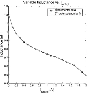
thereby changing the permeability of the core. Effectively, this changes the inductance seen in the signal path, and the device acts as an electronically-controlled variable inductor. The measured inductance vs. control current of the cross-field reactor used in the prototype system (described in Chapters 3 and 5) is shown in Fig. 2.4.
The cross-field reactor then allows control of the overall shunt-path inductance of the filter. In this way, it is possible to not only compensate for coupling mismatch of the coupled magnetic device, but to also cancel the parasitic inductance of the capacitor. Moreover,
by measuring output ripple performance and placing the coupling under closed-loop
con-trol, attenuation can be maximized under all operating conditions. The control strategy for the proposed active tuning approach is detailed in Chapter 4. Experimental results demonstrating the high performance of this approach are presented in Chapter 6.
Annular Coil Toroidal Coil
Figure 2.3: Structural diagram of a cross-field reactor. A single magnetic core is wound with two orthogonal windings, a toroidal coil and annular coil, which are not magnetically coupled.
-2.4 Adaptive Coupling Control
Variable Inductance vs. Yntrol
1.2 1.1 Q C. C 0 C: 0.9 0.8- 0.7-0.6 0.5 0.4L-0 0.2 0.4 0.6 0.8 1 1.2 1.4 1.6 1.8 2 1control [A]
Figure 2.4: Effects of varying control current on the cross-field reactor inductance.
E) experimental data
5 t order polynomial fit .
Chapter 3
Prototype System
3.1
Introduction
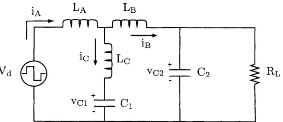
The control strategy proposed in Chapter 4 is presented in the context of a switching dc/dc power converter. A buck converter was chosen to validate the proposed control strategy. This chapter presents the prototype buck converter having a coupled-magnetic output fil-ter, as illustrated in Figures 3.1 and 3.2 and Tables 3.1 and 3.2. Section 3.2 describes the prototype buck converter, Section 3.3 presents the design guidelines for the adaptive coupled-magnetic filter, and Section 3.4 describes the buck converter voltage regulation.
3.2
Prototype Buck Converter
The buck converter operates under averaged current-mode control at a switching frequency of 400 kHz, and is designed to regulate the output at 14 volts (V) from a nominal input of 42 V. This conversion function is relevant to some emerging automotive applications, for example [19]. The converter is designed to support a load range of 16 watts (W) to 65 W. The complete buck converter schematic is presented in Appendix A.
In addition to the coupled-magnetic element (described in detail in Section 3.3), the output filter comprises capacitors C1 and C2. C1 is implemented as a 10 pF high-ripple,
low-Q
42 V +D D NDCfto
load L NACI Lvar C2Ci
Prototype System LA LB \/.f- . to load Q1 Lc 42
V +
D
LT a 2T~
LvaFigure 3.2: Model of buck converter and coupled magnetic filter.
inductance film capacitor (ITW Paktron 106K050CS4). C2 is implemented as a parallel
combination of a 20 pF polypropylene capacitor (Cornell-Dubilier 935C1W20K), a 2200 pF electrolytic capacitor (50V, RESR = 0.040Q), and a 0.1 pF ceramic capacitor. The large electrolytic capacitor appears resistive at frequencies of several kHz, and it was added to the output filter to provide additional damping to the inner and outer control loops at these frequencies. The capacitance comprises the electrolytic capacitor DC model, while its parasitic resistance, RESR comprises the AC model (Appendix A, Section A.4). Further-more, the capacitor also helps to provide additional holdup capacitance at the output. The non-magnetic output filter components are summarized in Table 3.1.
Additionally, a large 27 mF electrolytic capacitor was placed in parallel with the load (physically away from the converter output). This was done to represent the behavior of the battery that would be present in an automobile, for example, or the hold up capacitor that appears in many applications. Because this capacitor is in parallel with the remote load, away from the actual converter output, it does not have a significant impact on the converter output switching ripple or serve to attenuate EMI. The capacitor does, however, provide low-frequency voltage holdup during load transients.
3.3
Output Filter Design Using a Coupled-Magnetic Device
with Adaptive Inductance Cancellation
The end-tapped configuration of the coupled-magnetic device (Fig. 2.1b) was chosen and implemented with the two windings separated on the bobbin in such a way as to minimize the capacitance across them. One winding was wound on the top half, while the other was wound on the bottom half of the bobbin. An RM1O/I A315 3F3 core was used to construct the coupled-magnetic device. A turns ratio of 5:4 (NDC : NAC of Fig. 3.1) was used. For the
DC winding, AWG 12 wire was used, and for the AC winding, Litz 175/40 wire was used.
-3.3 Output Filter Design Using a Coupled-Magnetic Device with Adaptive Inductance Cancellation
C1 10 pF ITW Paktron 106K050CS4
C2 20 pF Cornell-Dubilier 935C1W20K
(parallel combination) 100V, Polypropylene
2200 piF Electrolytic, 50 V (RESR = 0.040Q)
0.1 pF Ceramic
Q
IRF1010E N-Channel Power MosfetD MUR302OWT Common Cathode Diode
Table 3.1: Device parameters for the buck converter of Fig. 3.2 (magnetics are detailed in Section 3.3 and Table 3.2).
The resulting coupled-magnetic device parameters are listed in Table 3.2. Experimental measurements indicate that the windings appear inductive for frequencies up to -11 MHz.
The variable inductor was designed such that its tunable range captured the inductance to be cancelled, namely the sum of the shunt-path inductance of the coupled-magnetic device and the parasitic inductance of the shunt-path capacitor. Construction of the variable inductor was as follows: two turns of the coupled-magnetic AC winding were wound conventionally on the bobbin of a P14/8 A315 3F3 core. The smallest size core within the practical design guidelines was desired. Thus, the smallest core that was able to handle the maximum ripple current and provide the proper tunable inductance range was chosen.
The control winding was constructed using 77 turns of AWG 28 wire wound through the center-post hole of the core (orthogonally to the inductance winding), as illustrated in Fig. 3.3. In order to reduce the control current required to partially saturate the variable inductor core, a high number of turns for the control winding was used. In principle, the geometry of the core is the main constraint for the maximum number of windings that can
be added.
Magnetics Tuned Coupled Magnetic Filter
Construction RM10/I, A315, 3F3 Core
5:4 Turns
LA 6.13 /H
LB 1.67 pH
LC - 0.82 pH
Table 3.2: Design parameters for the coupled-magnetic device. Inductances LA, LB, and LC correspond to those in Fig. 3.2.
Prototype System
variable condrng
inductance winding
Figure 3.3: Variable inductor.
3.4
Buck Converter Output Voltage Regulation
The buck converter is designed to regulate the output voltage at 14 V from a nominal input of 42 V. Averaged current-mode control is used to achieve the desired regulation. The
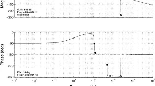
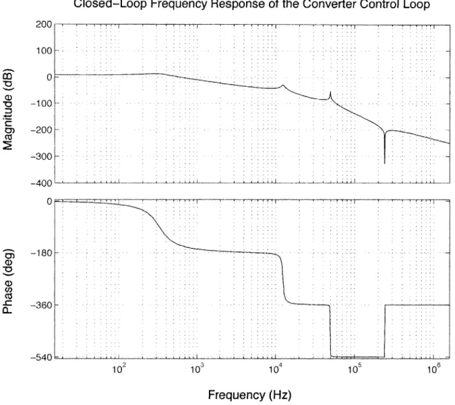
following figures illustrate the dynamics of the buck converter control circuitry. The full mathematical assessment of stability is presented in Appendix A. Figures 3.4 - 3.6 illustrate the control behavior prior to the addition of the large electrolytic capacitor damping leg. On the contrast, Figures 3.7 and 3.8 present the open loop dynamics of the converter inner and outer control loops following the addition of the capacitor. It can be seen from the open-loop Bode plots that both loops are now much better damped. The inner control loop
has a phase margin greater than 60 degrees and a gain margin greater than 20 dB, while the outer loop has a gain margin greater than 40 dB and a phase margin greater than 90 degrees. Thus, as can be seen in Fig. 3.9, the overall closed-loop response is well-behaved. The closed-loop poles and zeros of the buck converter control transfer function are shown in Table 3.3. Without the damping provided by the electrolytic capacitor, the system was stable, but small (~20 mV) ringing could typically be observed at the output, indicating poor damping. The loop transfer functions and the mathematical analysis used to describe the converter dynamics are presented in Appendix A.
Closed-Loop Poles [Hz] Closed-Loop Zeros [Hz]
- 8.55 -8.54 - 71.21 -2.12 1
i0
4 - 7.17 - 103 - 9.41 -104 - 4.47 ± 8.76 - 103j
- 4.32 ± 14.88 - 105 j - 2.45 ± 48.55 - 10 3 - 2.09 - 104 - 9.40 - 104Table 3.3: Poles and zeros of the closed-loop buck converter control transfer function.
-3.4 Buck Converter Output Voltage Regulation
Open-Loop Frequency Response for the Converter Inner Loop
-r
,
-o
L
G.M.: 8.85 dB Freq: 4.89e+004 Hz Stable loop __j ---_L_.jLL. L iI _ __ _ _ __ _ _ __ _ _ __ _ _ 10 1 10 106 10Frequency (Hz)
Figure 3.4: Open-loop frequency response of the buck converter the addition of the large electrolytic capacitor.
inner control loop prior to
1-1 m :0)' V 100 50 0 -50 -100 -150 -200 -250 0 Yi) CU -90 -180 -270 -360 P.M.: 14 deg Fr 4?:1.2 10 4 Hz--- ---10 0 10 2 10 3 10 4
Prototype System
Open-Loop Frequency Response for the Converter Outer Loop
1 0 - 7Jl -
7 1
T1
1 - - T r r - 7 7 ' r rr - -7-(-100-C
-200 -300 G.M.: 48.3 dB Freq: 6.06e+003 Hz Stable loop -400' 0 D-180---C -360K P.M.: 35.1 deg Freq: 297 Hz -540 10 10 10 102 103 10, 10 10 10Frequency (Hz)
Figure 3.5: Open-loop frequency response of the buck converter outer control loop prior to the addition of the large electrolytic capacitor.
-3.4 Buck Converter Output Voltage Regulation
Closed-Loop Frequency Response of the Converter Control Loop
106
103 104 10
Frequency (Hz)
Figure 3.6: Closed-Loop frequency response of the buck converter control loop prior to the addition of the large electrolytic capacitor.
2)00 100 CO C 0, I ~ I 0 -100 -200 -300 -400 0 0D CU, -180 -360 -540 102 - I I
-Prototype System
Open-Loop Frequency Response for the Converter Inner Loop
100 50 co -50 0) -100 . . ... -150 - G.M.: 21.1 dB Freq: 2.53e+004 Hz Stable loop -200 0-(D -180 ---P.M.: 63.8 deg Freq: 5.48e+003 Hz 100 101 102 103 10 105 106 107 Frequency (Hz)
Figure 3.7: Open-loop frequency response of the buck converter inner control loop following the addition of the electrolytic capacitor damping leg.
-3.4 Buck Converter Output Voltage Regulation
Open-Loop Frequency Response for the Converter Outer Loop
50 -50 _-100-- 1 50 --200 ---250 -G.M.: 40.4 d8s -300 -Freq: 6.54e+003 Hz Stable loop---35 0 100 101 102 10 104 10 106 10 0 -90 -180- -270--360 -450 -540 10 1Frequency (Hz)
Figure 3.8: Open-loop frequency response of the buck converter outer control loop following the addition of the electrolytic capacitor damping leg.
C: C 0) (D CD C/ -c - 7 P.M.: 94.3 deg Freq: 64.2 Hz
Closed-Loop Frequency Response of the Converter Control Loop
-, , , -10 1 10 2 10 104 10 10Frequency (Hz)
Figure 3.9: Closed-Loop frequency response of the buck the addition of the electrolytic capacitor damping leg.
converter control loop following
- 36 -Prototype System 100 50 0 C
0)
(D C,) -50 -100 -150 -200 -250 -3000r
-180 -360 -540Chapter
.4
Adaptive Control Methods
4.1
Introduction
The proposed adaptive inductance cancellation method relies on feedback control. The adaptive controller is presented here in the context of the buck converter described in Chapter 3. Sections 4.2 and 4.3 describe the mathematical control model for the adaptive tuning approach, while Section 4.4 describes the simulation used to verify the efficacy and the stability of the approach and presents the simulation results.
4.2
Control Strategy
The proposed design approach uses feedback control based on sensed buck converter output ripple to maintain good performance. The controller measures the root-mean-square (RMS) of the converter output ripple voltage (VRp e) and electronically tunes the inductance of the cross-field reactor to minimize the ripple seen at the filter output. A Lyapunov control strategy similar to those described in (8,20-22] has been implemented. The block diagram of Figure 4.1 illustrates the basic control strategy employed.
isin(wt)
f(Icontrol) = VRMS r
icntrl -kf
Adaptive Control Methods
The control method is integral in nature. The controller generates a small, exogenous, low frequency sinusoidal variation in the cross-field reactor control current that controls the shunt-path inductance. This consequently results in small variations in VRMS as the shunt-path inductance varies. The controller then correlates the changes in VRMp with the sinusoidal variation in Icontrol by multiplying the two and integrating the product. When the average value of the product is negative, Icontrol is below the optimal operating point and the integral is driven to increase Icontrol. Conversely, when the average value of the product is positive, Icontrol is above the optimal operating point and the integral of the product drives Icontrol down. At the optimal operating point, the average value of the integrator input is ideally zero and the operating point is maintained.
The small sinusoidal signal is added to the negated output of the integrator and the sum is used as the control current to the variable inductor. This control strategy drives the
DC component of the control current to the minimum of the VRM vs. Icontrol function,
where the integral output holds constant. The control method assumes that the RMS value of the output ripple as a function of Icontrol is unimodal in the range of interest. Experimental measurements confirm this assumption for the prototype system described in Chapter 3 (Fig. 4.2). The close-fitting 4th order polynomial helps to further demonstrate
the unimodal behavior of the function on the control current range of interest.
VRMSV. V RVSvs.l 1.8 ripple control 1.7 -.e- experimental data 1.6 4 order fit 1.5 1.4 1.3 1.2 -> 0.9 - - -2' 0.8-->0.40.6 0.5 .. -. .. -0 .4 . -.. . .. -.. .. 0 .3 --. ... . .. . . .. ...--. 0.2 0.1 -0 0 0.1 0.2 0.3 0.4 0.5 0.6 0.7 0.8 0.9 1 1.1 Icontrol [A]
Figure 4.2: Scaled VRMS ripple as a function of the variable inductor control current for the prototype system (as measured at the output of AD637 of Fig. 5.2) and its 4th order
polynomial fit.
-4.3 Stability Analysis of the Control Method
The function of Fig. 4.2 was obtained by manually controlling the value of the cross-field reactor control current and measuring VRMS ripple, A power supply was used to inject theM desired amount of DC control current into the control windings. VRMp i was measured
using the AD637 RMS-DC converter IC located on the adaptive cancellation controller board (described fully in Chapter 5). The scaling factor of 148.3 at the switching frequency reflects the gain of the high-pass filter stage at the input of the AD637 (Fig. 5.2).
4.3
Stability Analysis of the Control Method
The proposed control approach is inherently stable. Consider the local average dynamics [23] of the system in Fig. 4.1 over an averaging period of the sinusoidal variation:
dzntrit) -k
ft(Isin(wT)
- f(Isin(WT) + icntrl(T) dT (4.1)dt T Jt
-Observing the function f(Tcntri(t)) = VR M of Fig. 4.2 and the control function of Eq. 4.1, it is evident that at the minimum of
f,
J, dtdictri(t) tends to zero. Thus, the minimum of theVrpe vs. icntri(t) function, 1cntr, is an equilibrium point of the system.
On the region of the state-space that contains the equilibrium point, the requirements for a Lyapunov function, V(Tcntri(t)), are the following [24]:
1. V must be continuous.
2. V must have a unique minimum at Icntri.
3. The value of V must not increase along any trajectory of icntri(t) on the state-space that
contains
IcntrI-Consider the function f(Tcntri(t)) = Vrip e as the Lyapunov function of the system. Fig-ure 4.2 confirms that the function meets the first two requirements. To demonstrate that the third requirement is also satisfied, consider the control strategy of Fig. 4.1 and Eq. 4.1. Taking the local average output of the integrator as the state variable of interest, it is observed that the trajectories of Tcntri(t) can only tend toward the minimum, forcing V to
decrease. Therefore, the function f(Tcntri(t)) = VRM of Fig. 4.2 is a Lyapunov function of the system and icntri is a stable equilibrium point.
Adaptive Control Methods
4.4
Simulation
To validate the efficacy of the control strategy, a time domain simulation of the approach was implemented in Simulink (Mathworks Inc., Cambridge, MA) as shown in Fig. 4.3. The complete Simulink implementation of the control approach is illustrated in Appendix B. A simplified average state-space model was developed for the buck converter (described more fully in Section 4.4.1), and is represented by the Icontrol to Vrippie block. The effects of varying the control current on the value of the variable inductance were determined empirically and modeled with a close-fitting 5th order polynomial (Fig. 2.4). Transfer function blocks
reflecting the dynamics and characteristics of circuit components to be used in the design of the physical control circuitry (Chapter 5) were derived for the controller. The model was then used to assess the dynamic performance of the controller.
121
0. . control ripple 2
O.5sin(27r. 5001;___
Voltage to Current High-Pass RMS BLOCK IC Saturation
Conversion Gain Stage Gain
Voltage LimitingMutpirGn
Block Mu t plier Gain
7_ IC Saturation
F 9 VI +12V
I_~ L. -kf +- _f-- 1
1, Vz -12 VIF
Figure 4.3: Simulink model of the proposed control control strategy.
4.4.1 Buck Converter State-Space Model
The simplified model of the buck converter, shown in Fig. 4.4, was used to develop the state-space model used in Simulink. An average state-space model was used to simulate the dynamics of the converter. The buck converter input filter was ignored, as it was designed in such a way as its dynamics did not interfere with those of the rest of the converter. Only the essential components of the output filter were included, and the parasitics present in the system were ignored for the purposes of the model. The average voltages across the two capacitors, vcl and vc2, and the average currents through the inductances LA and LC were chosen as the state variables.
The signal Vd represents the voltage seen at the diode cathode (Fig. 3.2). This signal is
-4.4 Simulation iA LA LB 1B
Vd
ic
LC
v
VC,
C,
2 C2 RLFigure 4.4: Simplified time-averaged model of the buck converter space model of Eq. 4.2.
used to obtain the
state-modeled as a square pulse with the frequency of 400 kHz, which corresponds to the converter operating frequency, an amplitude of 42 V corresponding to the nominal converter input voltage, and a duty ratio of -, which provides the 42 V to 14 V conversion function. The passive components reflect the converter output filter, and their values are detailed in Tables 3.1 and 3.2. It must be noted, however, that the output filter capacitor C2 does not
include the 2200 pIF electrolytic capacitor damping leg or the 0.1 /-F ceramic capacitor. The value of 8 Q was used for RL, corresponding to 35% of converter maximum power. From the model of Fig. 4.4, the following state-space description of the converter was obtained:
0 0 LALB+ LALC -LB + LBLC 0 0 -(LA + LB) LALB + LALC + LBLC 0
_L
1 -1 C2 C2 0 0 -LC LALB + LALC + LBLC LA LALB + LALC + LBLC 0 -1 RC2 LB + LC LALB + LALC + LBLC LB LALB + LALC + LBLC 0 0 S ic vC1 VC2 vC1 VC2 + Vd (4.2)Adaptive Control Methods
The model of Eq. 4.2 assumes that the variable inductance of the cross-field reactor changes slowly relative to the rest of the system. The slow time change of the variable inductance was, in fact, taken as a requirement in the design of the adaptive cancellation control circuitry. The use of the slow-varying (500 Hz) sinusoidal signal to sweep the VRMS ripple vs.
Icontrol function and the integrator in the feedback path (Fig. 4.3) forced the dynamics of the control to be slow compared with the dynamics of the converter. This design strategy ensured that the variable inductor included in the output filter of the buck converter could indeed be treated as time-invariant for the purposes of the buck converter dynamics. Thus, it was included in the overall shunt-path inductance, LC. The Simulink diagram of the model in Eq. 4.2 is shown in Appendix B.
4.4.2 Simulation Parameters
The final simulation model of Appendix B was used to assess the dynamics and stability of
the control strategy, with the following simulation parameters:
Simulation Time 0 - 0.5 seconds
Fixed Step Size 2.5 -10-8 seconds
Solver Method ode5 (Dormand-Prince)
Stored Data Decimation Rate 10000
Table 4.1: Control model simulation parameters.
The largest allowable step size was chosen for the simulation. The switching frequency of the buck converter, reflected in the input variable Vd of Fig. 4.4 and the pulse of Fig. B.2 provided the upper boundary on the magnitude of the step size. The simulation data were decimated by a factor of 10000 due to the large size of the files provided by simulation. This forced signals such as the converter output ripple to appear undersampled. However, since the dynamics of the adaptive cancellation control are on the time scale of hundreds of milliseconds, the decimation did not prove detrimental to the simulation analysis. The simulation time of 0.5 seconds ensured that the system had reached steady state.
4.4.3 Simulation Results
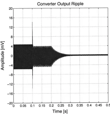
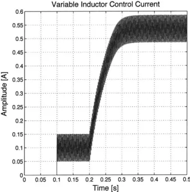
In order to view the effects of the adaptive inductance cancellation, the converter was first allowed to reach steady state. The adaptive tuning was then enabled at time t = 0.1
seconds. This was performed by multiplying the control current by a step function with a
-4.4
Simulation
delay of 0.1 seconds (Fig. B.1). The simulated transient behavior of the control current, the converter output ripple, and converter VRMS are depicted in Figs. 4.5 - 4.7.
Simulation results indicate that the proposed active tuning control method exhibits good static and dynamic behavior. A factor of 20 reduction is predicted for the converter output ripple (Fig. 4.5) and for VRMS (Fig. 4.6) when Icontrol reaches its DC steady state value of
0.53 amperes (A) (Fig. 4.7) after approximately 200 milliseconds (ms).
The simulated average steady state control current, icntrl, matches that predicted by the manual tuning of Fig. 4.2 within the limits of the model. The converter output voltage ripple, and VRMS , however, are predicted to be lower than experimental manual tuning
results suggest. These discrepancies may be attributed to the unmodeled parasitics of the prototype system.
Converter Output Ripple
16 12 8 5, E (D E
L
-A 0.05 0.1 0.15 0.2 0.25 0.3 Time [s] 0.35 0.4 0.45 0.5Figure 4.5: Simulated transient performance of the converter output ripple as active tuning is enabled at time t = 0.1 seconds.
-8- -12- -16--20' 0 ... .- .. .. .. .-.-.-. .-.- .-... . .. . . . ... . . . .. . . .. . . . .. . . .. . . . .. . . . .. . .. . . . . .. . . . .. . . .. . . . ... . . . ... . . . .. -. . .. ...-. -.-.-.-. . ... ... ..
Adaptive Control Methods
Converter Output Ripple RMS
8 7 6 55 E (D 4 C3 2 1 0 .5 8 .5 7 .5 6 .5 5 .5 4 .5 3 .5 2 .5 - -... . -. .. . -..-.-.-.5 -- - - - -0 0.05 0.1 0.50.2 0.25 0.3 0.35 0.4 0.45 0.5 Time [s]
Figure 4.6: Simulated transient performance of the RMS of the converter output ripple, VRMS as active tuning is enabled at time t = 0.1 seconds.
0.6 0.55 0.5 0.45 0.4 <0.35 0.3 E 0.25 0.2 0.15 0.1 0.05
Variable Inductor Control Current
0 0.05 0.1 0.15 0.2 0.25 0.3 0.35 0.4 0.45 0.5 Time [s]
Figure 4.7: Simulated transient performance of the variable inductor control current as active tuning is enabled at time t = 0.1 seconds.
- 44 ---. ..-. .-. ..-. .-. -.-. .- . --- ... .. .... .-.-.- .- -. -- ... ---... - ... -... . .... . -. .. ... ... ... . - - --. ... . -. .. ...- .. .... .. -. -. .-- ..--.......... ... -- - - ...-. - --... --.-.- -.-.-.-.-.-.. - -- -- - - -. - - . -.~~~~~~~~~~~~~~~~~~~~ - . -. -... ...-- -- . .-. ...
--.
....
....
-.
.
.-
.
-.
....
....
-. ..-.
.-.
.
.
..
..
...
.
.-...
.
..-.
.
-
.
...
...
-
-.
-..
..
..-..
..
..
...
-..
. . . ....-..
-- - -- - - ... --- ......--...Chapter 5
Controller Implementation
5.1
Introduction
The proposed control strategy of Chapter 4 was implemented on a printed circuit board (PCB) using standard circuit components, as illustrated in Fig. 5.2. This chapter details the design of the adaptive inductance cancellation control board circuitry. Section 5.2 outlines the design guidelines for the control board and Section 5.3 describes the implementation of the control board circuitry.
5.2
Control Board Design
The diagram of Fig. 5.1 illustrates the relevant blocks of the control circuitry and the ap-proximate signals levels at the input and output of each block. The signal levels correspond to a buck converter system having an adaptive coupled-magnetic output filter. The control current for the variable inductor is assumed to be in the range of 0.05 - 0.95 A. These
conditions determine the range of the converter output ripple amplitude to be 5 - 40 mVpp. The output of the buck converter constitutes the input to the system. The differential high-pass filter serves to isolate the ripple from the converter output signal and to provide additional gain. The gain is required by the AD637 RMS-DC converter in order to ensure adequate bandwidth. The differential high-pass filter was implemented in two stages in order to yield appropriate gain and bandwidth. The resulting gain of the high-pass stage in the range of the first two harmonics of the switching frequency (400 kHz - 800 kHz) was
measured to be 148.3.
In order to increase the signal-to-noise ratio at the output of the AD633 multiplier a gain of 4.73 was incorporated. A gain of -1000 (at 1 radian/sec.) was added to the integrator to increase the response speed of the system, resulting in the following transfer function: -1000. The 1 - 9 V voltage limiting circuitry was added to maintain the variable inductor control
Controller Implementation monolithic function generator XR2206 differential _ 0.5 -0.5 V high-pass filter R MS-DC -0.5 -0.5 V gain =148.3 converter 5 -40 mVpp AD637 AD633
f
buck converter quadrature integrator voltage limiting adder
output multiplier gain = -1000 circuitry gain = 1
gain = 4.73 (at 1 rad/s)
0.05 -0.95 A 0. .
Lvar 4= _0.5 - .
variable voltage to current inductor converter
gain = 0.1
Figure 5.1: Block diagram of the adaptive inductance cancellation control circuit.
and the scaling of the resulting sum by 0.1 during the voltage to current conversion. The variable inductor current was chosen to be in the aforementioned range because this range was experimentally confirmed to contain the minimum of the VRIM rippleVS vs. 'control cnrlfnto function
(Fig. 4.2).
Finally, the amplitude of the sine wave at the output of the XR2206 monolithic function generator was chosen such that it produced enough variation in the variable inductor control current signal to induce a change of -10 - 20 mV at the output of the AD637 near the
optimal operating point, cntr, of the VripMpe vs- Icontrol function. Thus, the value of 0.5 V was chosen for the amplitude. However, in practice, a slightly smaller amplitude could also have been chosen, without negatively affecting the control performance.
5.3
Control Board Circuitry
The blocks of Figures 4.3 and 5.1 are implemented as follows: the sinusoidal variation is implemented using an XR2206 monolithic function generator. An AD637 RMS-to-DC converter is used for the RMS block and an AD633 multiplier for the product block. Ad-dition, integration, buffering, and voltage to current conversion are performed using the LF347 quad operational amplifier. The variable inductor control current is provided using a TIP29C NPN power bipolar transistor. A zener diode and the LM317 adjustable voltage regulator serve to constrain the voltage at the output of the integrator in the range of 1
-5.3 Control Board Circuitry
9 volts. Finally, a differential high-pass stage is added using two LM6361 wide bandwidth
operational amplifiers to provide additional gain and to decouple the DC component of the output from the control circuitry. The resulting control circuit schematic is illustrated in Figure 5.2.
The circuit of Figure 5.2 was implemented on a printed circuit board using the Eagle (CadSoft Computer GmbH) layout editor. A four layer, FR4 PCB was used for the control board. The Eagle circuit schematic and the masks for each of the resulting layers of the printed circuit board are included in Appendix C.
1.5kQ 001pF 1000 power converter 1 output + 0.01pF 1000 1.5k0 1.5kQ 0, 01pF LM63 differential high-pass stage amplitude adjust. S *3 16kQ .. . -- - 5 0.1pF 6 7 frequency adjust. 121kQ - 8 ---- NC-13 6 XR2206 MO W1 TC1 TC2 TR1 W2 SIN TR2 AD637 Vin absolute value Vn squarer/divider 25kQ
~
25kQ RII DEN - OUTAdB Filter Cav
13 1 14 1TH D adjust 1N4001 3900 Lvar 11kQ _-MM- +LF347. ' - LF347b TIP29C 11k k 'f 11kQ k 1Q/1W 11k11 f ._. AD633 0.068 1F voltage limiting ikO 15kQ circuitry - W 7 (1.08 - 9.1 V) +
~L
347c + r - ----+ LF347d. +-9 --- 3 + -1N4739 8jj pF !47k0 - LM317 1N4001 multiplier -- ----averaging gain adjust. + 12 V Vi IV
capacitor
AJ 240Q regulator
output (1.68 V)
82Q
Figure 5.2: Schematic of the control board circuitry.
00