1
Correlative elemental and electrical micro-analysis of laser fired
contacts in silicon solar cells
by
Patricia Yen
B.S. in Engineering Physics
B.A. in Luso-Brazilian Language and Literature
University of California, Berkeley, 2014
Submitted to the Department of Mechanical Engineering
in partial fulfillment of the requirements for the degree of
Master of Science in Mechanical Engineering
at the
MASSACHUSETTS INSTITUTE OF TECHNOLOGY
September 2016
2016 Massachusetts Institute of Technology. All rights reserved.
Author………
Department of Mechanical Engineering
August 4, 2016
Certified by………
Tonio Buonassisi
Associate Professor of Mechanical Engineering
Thesis Supervisor
Accepted by……...………
Rohan Abeyaratne
Professor of Mechanical Engineering
Chairman, Department Committee on Graduate Theses
2
Correlative elemental and electrical micro-analysis of laser fired contacts in silicon solar cells
by
Patricia X. T. Yen
Submitted to the Department of Mechanical Engineering on August 4, 2016 in Partial Fulfillment of the Requirements for the Degree of Master of Science in
Mechanical Engineering
ABSTRACT
Photovoltaic (PV) energy is an abundant and clean alternative to conventional energy sources, which pose an irreversible threat to the environment. For PV to reach cost parity with conventional energy, advances like laser-fired contacts must be adopted to improve cost levers like solar cell efficiency and industrial throughput.
This work examines the relationship between laser-processing on the structure and property of solar cells, with the goal of (1) characterizing the differences between using two lasers simultaneously (double-shot lasing) versus a single laser for LFC processing, and (2) using the new findings to optimize industrial LFC efforts. Electrical properties such as lifetime degradation and contact resistance are evaluated using photoluminescence imaging and transmission line measurements, respectively. LFC structures are studied using scanning electron microscope and elemental mapping tools like micro-X-ray fluorescence microscopy and energy dispersive spectroscopy.
For the conditions studied, it is unclear whether double-shot lasing can produce higher-quality LFCs than single-shot lasing, although results suggest that the infrared laser influences electrical properties more than the green laser. For future LFC optimization, the µ-XRF maps of elemental distribution may offer a novel way to evaluate LFC formation.
Thesis Supervisor: Tonio Buonassisi
Title: Associate Professor of Mechanical Engineering
Thesis Supervisor: Ian Marius Peters Title: Research Scientist
3
A
CKNOWLEDGEMENTS
I would like to express a tremendous amount of gratitude to those who have been part of my graduate school journey. It has been a rewarding and challenging experience, and I could not have done it alone.
I would like to thank my family. I would not be where I am now without their love and support.
I would like to thank Prof. Buonassisi for his encouragement and time. It has been inspiring to work in the PV Lab and see the depth and range of impact one person can have.
I would like to thank the supportive and kind members of the MIT PV Lab for helping me learn and grow as a scientist. I would like to especially like to thank those who have been contributed to my thesis work: Ashley Morishige, who answered my questions with thoroughness and shared her expertise and support at the synchrotron; Mallory Jensen, for her support and mentorship that guided me along the project; Dr. Sergio Castellanos, for teaching me to conduct and interpret results from energy dispersive spectroscopy; Dr. Austin Akey for his guidance and expertise throughout the project; Dr. Tim Kirkpatrick for his mentorship; Dr. Maulid Kivambe for teaching me to conduct and interpret results from the scanning electron microscope; and Dr. Marius Peters for close reading of my thesis.
I also deeply appreciate the efforts of Dr. Steve Hegedus, Dr. Jianbo He, and Mr. Ujjwal Das for fabricating the samples for this study; Dr. Marco Mendes and Dr. Xiaoyong Song for laser processing the samples; and these five individuals for insightful discussions and experimental analysis. I also want to thank Dr. Barry Lai at Argonne National Laboratory for assistance in processing the µ-XRF data.
Last but not least, I am thankful to the many faces of MIT and Cambridge where I have found friendship, community, and help.
This research was made possible by funding from the National Science Foundation Graduate Research Fellowship Program and grants from the National Science Foundation and the U.S. Department of Energy.
4
A
BBREVIATIONS
Abbreviation Description
Ei Initial energy level of an electron
Eh Higher energy level of a n electron
Eg Bandgap energy
SRV Surface recombination velocity
J0 dark saturation current density
JL photogenerated current
J net current density
V voltage applied acrossd diode q Charge of an electron
k Boltzmann’s constant T Absolute temperature
VOC Open-circuit voltage
I-V Current-voltage
JSC Short-circuit current density
Jmpp Current density at the maximum power point
Vmpp Voltage at the maximum power point
FF Fill factor
Pin Total power density of incident radiation
Al-BSF Aluminum back surface field PERC Passivate emitter and rear contact
IBC Interdigitated back contact LFC Laser-fired contact
IR infrared SiNx Silicon nitride
PCD Photoconductance decay
PC-PLI Photoconductance-calibrated photoluminescence imaging RF Radio frequency
QSS Quasi-steady-state CCD Charge-coupled device
τeff Effective minority carrier lifetime
τbulk Bulk minority carrier lifetime
τs Surface minority carrier lifetime
W Wafer thickness
S Surface recombination velocity
Dn Diffusivity constant
TLM Transmission line measurement
RC Contact resistance
RT Total resistance
l Distance between measured contacts in TLM
RSK Modified sheet resistance under contact
5
w Width of contact
EDS Energy dispersive spectroscopy SEM Scanning electron microscope
µ-XRF Micro-x-ray fluorescence spectroscopy a.u. Arbitrary units
6
C
ONTENTS
Abstract ...2 Acknowledgements ...3 Abbreviations ...4 Contents ...6 Figures ...8 Tables... 10 1 Introduction ... 11 1.1 Motivation ... 11 1.1.1 Objectives ... 111.1.2 Basics of silicon solar cells ... 11
1.1.3 State of the art of PV contacts ... 16
1.1.4 Next generation cell architectures ... 18
1.2 Background of Laser-Fired Contacts ... 19
1.2.1 LFC lasing process ... 20
1.2.2 LFC state of the art ... 22
1.2.3 Previous LFC characterization efforts ... 23
1.3 Current challenges to implementing LFC’s in the market ... 25
1.4 Approach... 26 2 Methods ... 27 2.1 Sample preparation ... 27 2.2 LFC Lasing Parameters ... 29 2.3 Characterization Techniques ... 30 2.3.1 Electrical Characterization ... 30
2.3.1.1 Photoconductance-calibrated Photoluminescence Imaging (PC-PLI) ... 30
3. Experimental Results ... 31
3.1 PL Images ... 31
7
3.3 µ-X-ray fluorescence spectroscopy for elemental mapping ... 34
3.4 SEM and EDS ... 36
4. Discussion ... 39
4.1 Expected property-process relationships of two-laser firing ... 39
4.2 Structure-property-process relationships ... 40
4.2.1 Property-process relationship: PLI measurements ... 40
4.2.3 Property-process relationship: TLM measurements ... 42
4.2.2 Structure-property-process relationship... 43
4.3 XRF vs. EDS ... 49
5. Summary & Conclusion ... 51
8
F
IGURES
Figure 1 The basic elements of a solar cell include contacts, an absorber, and a junction that separates charge carriers. Image modified from [11] ... 12 Figure 2 I-V curve for an illuminated cell ... 15 Figure 3 An image of the cross-section of the rear aluminum contact and the eutectic layers in an Al-BSF cell [10] ... 17 Figure 4 A comparison of the LFC process and the localized contacting process for point contact patterning on passivated rear silicon solar cells [30]. ... 19 Figure 5 A figure showing the bulk silicon, passivation layer, and aluminum layers in a laser-fired contact material stack. [48] ... 20 Figure 6 A scanning electron micrograph (SEM) (left) and optical profilometry measurement (right) showing the characteristic inner crater and outer aluminum ring for an LFC fired with a microsecond pulse. [69] ... 23 Figure 7 The material stack of the samples used to test different LFC lasing parameters. The layers are not to scale. ... 28 Figure 8 A diagram showing the rear of the sample. Individual LFC spots were fired into the metallized strips. Each row corresponds to a new lasing condition. The dimensions are not to scale. ... 29 Figure 9 PL images of one sample taken (a) before laser processing, (b) after lasing processing with sampled linescans shown in color, and the corresponding plot of PL intensity shown for the linescans. ... 32 Figure 10 A row of LFC strips that is used for TLM measurements. One data set corresponds to the resistance measurements between one strip and every other strip. ... 33 Figure 11 The material stack of the samples used to test different LFC lasing parameters, with the incident laser and lased region shown. The layers are not to scale and the thicknesses are listed in 2.1 Sample preparation(pg. 26). ... 39 Figure 12 A plot of PLI contrast values versus the green laser energy dose, showing that PLI contrast primarily depends on the IR laser. ... 41
9
Figure 13 The RC data from Table 3 plotted against green energy dose. Group 2 corresponds to the
red symbols, and Group 3 corresponds to the blue symbols. Group 1 is not shown because contact was not measured. ... 43 Figure 14 (a) EDS maps, (b) µ-XRF maps, and (c) two SEM images of the same“IR 2” spot, which highlight different features. The scale bar shown applies to all maps. The same µ-XRF maps were shown in Table 4 (34), but in log10 scale. Here, the maps are linear. ... 49
10
T
ABLES
Table 1 A summary of the four lasing parameters used to fire LFCs in this study. ... 29
Table 2 Contrast values for different lasing conditions.. ... 33
Table 3 RC for different lasing conditions as measured by TLM. ... 34
Table 4 µ-XRF maps showing counts for silicon, aluminum, antimony, titanium, and Si:Al. ... 35
Table 5 The Si:Al values for each of the lasing conditions ... 36
Table 6 SEM images showing contacts that were fired with each lasing condition. ... 37
Table 7 SEM images of larger LFC and smaller LFCs ... 42
Table 8 The tested lasing conditions are categorized into Group 1, Group 2, and Group 3 ... 44
Table 9 Data for Group 1, along with SEM images and XRF maps ... 45
Table 11 Selected SEM micrographs and data of Group 1 conditions. ... 47
11
1 Introduction 1.1 Motivation 1.1.1 Objectives
Anthropogenic carbon dioxide emissions pose an urgent threat to the environment and global human development [1], [2]. Conventional power plants are the largest source of U.S. emissions, accounting for 40% of American greenhouse gas pollution [3]. While solar energy is an abundant and clean alternative, the cost of photovoltaic (PV) manufacturing remains a significant barrier to its widespread deployment [4]. For utility-scale and subsidy-free adoption, manufacturing costs for the standard silicon PV modules must drop to $.75/W to reach cost parity with conventional energy sources [4], [5]. This translates into a need for cheaper, scalable processes that can simultaneously push PV technology past the current industry average of 16% cell efficiency [6].
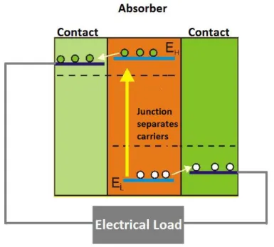
Since their invention in the 1950s, silicon solar cells have dominated the photovoltaic market [7]. To extract charge, metal contacts are typically applied to silicon solar cells using a relatively simple screen-printing process [8]. Because cost is strongly correlated with cell efficiency, higher-efficiency PV device architectures have emerged. These require local contacts, which involve local alloying of metals through a passivation layer [9]. The foundational study of laser-metal-dielectric-silicon interactions becomes important for understanding and optimizing local contact formation. 1.1.2 Basics of silicon solar cells
In a solar cell, incident light produces a voltage difference at the junction of two different materials. This effect is called the photovoltaic effect, which what makes a solar cell work. A solar cell consists of at least three basic elements: an absorber, a junction, and contacts. The photovoltaic effect can be considered as three basic processes, which take place in the solar cell:
1) An absorber (typically silicon) absorbs incoming photons, and charge carriers are generated
2) A junction facilitates charge carrier separation
3) Contacts at the junction terminals collect carriers and pass them through to an external load [10]
12
Figure 1 The basic elements of a solar cell include contacts, an absorber, and a junction that separates charge carriers. Image modified from [11]
When a photon is absorbed by a material, the photon’s energy excites an electron from an initial energy level (Ei) to a higher energy level (Eh). Photons can be absorbed and generate an
electron-hole pair if the photon energy exceeds the bandgap energy (Eg). This process is shown for
an ideal semiconductor in Figure 1.The excitation of the electron to the higher energy level results in a hole, which behaves like a positively charged particle. Consequently, the absorption of one photon results in an electron-hole pair.
The electron-hole pair can recombine, meaning that the electron can relax back to the valence band and eliminate the hole. This is a non-ideal process that limits the separation and collection of free carriers. This can happen through radiative recombination, when the energy is released as a photon, or non-radiative recombination, when the energy is transferred to other charge carriers or lattice vibrations. To prevent recombination, the absorber should have selective interfaces on both sides that allow only one type charge carrier to flow out of each. This means that electrons can only exit the absorber on one side, and holes can only exit the absorber on the other side. Silicon solar cells use n- and p-type material as the selective interfaces.
13
1) Radiative recombination is the reverse process of absorption. An electron that is in a higher non-equilibrium energy state emits a photon and relaxes back to an empty lower-energy state. The energy of the photon is equal to the difference in energy states.
2) Auger recombination involves an electron recombining with a hole and emitting extra energy to another electron, rather than a photon.
3) Shockley-Read-Hall recombination involves elemental impurities and structural defects that introduce energy levels into the band gap. These defect levels create a two-step recombination process, in which electrons relax from the conduction band energy state to the defect level, then combine with a hole in the valence band. In the case of thermally oxidized silicon, the surface recombination velocity is in the range of 1-10 cm/s for doping impurities <1017 cm-3 [12]. For larger concentrations, the SRV increases rapidly [13].
Recombination occurs in the bulk and surface of a semiconductor. The bulk refers to material characterized by uniform properties, as measured in sections that are sufficiently far from a sample’s boundaries [14]. The surfaces of semiconductors are sites of severe defects in the crystal structure and introduce a large density of defect states within the bandgap. In a silicon wafer, surface interfaces arise when silicon abruptly encounters either a metallized or non-metallized surface. Metal-silicon interfaces can result in more than 50% of losses due to recombination in high-efficiency cells and exhibit very high surface recombination velocities (SRVs), which define the rate of recombination at surfaces [6], [15]. In semiconductor heterostructures, interface recombination occurs by the same mechanism [16]. At interfaces, SRV can significantly reduce solar cell efficiency and is mainly affected by the density and character of interface states [17].
SRV is largely influenced by the density and types of defect states that are introduced by dangling silicon bonds at the surface. To reduce these defect states, a process called “passivation” is used to protect the surface of a semiconductor. Chemical passivation creates a layer of material that saturates the dangling bonds at the surface [16]. Passivation layers at interfaces are ideal because they can minimize carrier recombination and improve minority carrier lifetimes. There are two ways to passivate silicon. One way is by chemical passivation of the surface, while the other way involves the field effect.
In field-effect passivation, a potential barrier can prevent minority carriers from reaching the surface [18]. The standard passivation method is thermal oxidation at a high temperatures to
14
grow a dielectric film. During the oxidation process, the interface between the oxide and silicon moves into the relatively defect-free bulk, reducing the density of interface states [17].
Chemical passivation involves the immersion of silicon wafers into liquids that can saturate the dangling silicon surface bonds. This occurs by using thin chemical oxide layers or hydrogen-termination to cover the surface [19]. In hydrogen-hydrogen-termination, the native silicon diode is first etched off the silicon surface using a hydrogen fluoride solution. The resulting surface silicon atoms are covalently bonded to hydrogen [20]–[22]. This passivation method does not persist and can only saturate the surface bonds for a short period of time [23].
When the diode is illuminated, the photovoltaic effect drives current through the device [24]. Photogenerated carriers result in a current as electrons move to the n-type side and holes to the p-type side of the junction. Under short-circuit conditions, charge does not build up and carriers exit the device as photogenerated current.
The current-voltage characteristics of a pn-junction can be approximated using the one-diode equation:
𝐽 = 𝐽L − 𝐽0(𝑒𝑛𝑘𝑇𝑞𝑉 − 1 ) Eq. 1
Here, J0 represents the dark saturation current density, or the diode leakage current density when
unilluminated, J is the net current density that flows through the diode, JL is the photogenerated
current, V is voltage applied across the diode, q is the charge of an electron, k is Boltzmann’s constant, and T is the absolute temperature [25].
Under illumination, photogenerated carriers build up as electrons on the n-type side and holes on the p-type side. This charge separation creates an electric field that opposes the existing electric field in the junction, which reduces the net field and allows current to flow.
Under open-circuit conditions, the forward bias of the junction increases to a point where resulting net current is zero. The voltage needed to balance these currents is called the “open-circuit voltage,” or VOC.
The external electrical characteristics of a solar cell are determined by illuminating the solar cell under standard testing conditions and measuring the current while biasing the cell at the
15
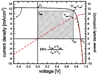
terminals. An example of the resulting I-V curve can be seen in Figure 2 I-V curve for an illuminated cell.
Figure 2 I-V curve for an illuminated cell
The primary I-V parameters are:
- JSC, or the short-circuit current density, which is the current generated at zero voltage. JSC
is determined by optical and recombination losses.
- VOC, or the open-circuit voltage, is the voltage generated at zero current. VOC is the
maximum voltage available from a solar cell and corresponds to the amount of bias on the cell. VOC occurs at short-circuit current conditions and can be found by setting the net
current equal to zero in the one diode equation:
𝑉OC = 𝑛𝑘𝑇 𝑞 𝑙𝑛 (
𝐽L 𝐽0
+ 1) Eq. 2
VOC is determined by the material bandgap, carrier recombination, and temperature
- Jmpp and Vmpp, the current density and voltage at the maximum power point (mpp) of the
I-V curve
- FF, or the fill factor, which refers to the largest rectangle that will fit in the I-V curve of a diode.
16 𝜂 = 𝑃max 𝑃in = 𝑉OC𝐽SC𝐹𝐹 𝑃in = 𝑉mpp𝐽mpp 𝑃in Eq. 3
where Pin is the total power density of the incident radiation. Under standard testing conditions,
Pin is taken to be 1000 W/m2.
The maximum power output of a solar cell is defined by VOC, JSC, and FF. Since JSC is
already near its maximum, VOC can only be increased by decreasing J0. J0 is directly related to
recombination, which was described earlier in this section. From Eq. 2 and Eq. 3, it is clear that increased recombination limits VOC and power conversion efficiency [26].
1.1.3 State of the art of PV contacts
Since their invention in the 1950’s, crystalline silicon solar cells have dominated over 80% of the PV market [27]. In industry today, the standard architecture for a silicon solar cell is the co-fired, screen-printed aluminum back surface field (Al-BSF) cell. The top layer on the front of an Al-BSF cell is doped to form a pn-junction and to allow electrical conduction to efficiently transport majority carriers to the contacts. A passivation layer is grown on top of the silicon, then metal contacts are screen-printed on so the silver paste punctures the passivation layer and contacts the silicon. An array of busbars and contact fingers are soldered on for carrier transport [28].
The rear side of an Al-BSF cell is fully metalized for efficient carrier transport. A small percent of the area is used for contact pads that are screen-printed as in the front contacts. The remaining area mixes with the underlying silicon to form a homogeneous mixture, or a eutectic, which provides low contact resistance and a passivating back-surface field. Because of its long-standing use, screen-printing electrical contacts is advantageous because equipment is widely available and continually improving. Compared to new contacting methods, screen-printing offers lower risk and capital investment for new manufacturing operations, as experience and equipment are both accessible.
17
Figure 3 An image of the cross-section of the rear aluminum contact and the eutectic layers in an Al-BSF cell [10]
Despite the simplicity and popularity of screen-printing, it presents limitations that impede the cost reduction of photovoltaics. The commercial success of photovoltaics is contingent upon cost, which can be targeted using three levers: material cost, efficiency, and manufacturing cost [27]. One major disadvantage to screen-printing is wafer warping, which imposes a bottom limit on the first cost lever, material cost [29]. After a silicon wafer is screen-printed with a metal paste, it is fired at a high temperature and cooled to form a eutectic and the BSF, as seen in Figure 3. The silicon cools and recrystallizes to form a BSF that enables low recombination around the contacts [30]–[32]. During this cooling process, the silicon warps significantly, inducing low mechanical yield that worsens significantly with thin wafers.
As wafer thickness approaches 100-200 μm to reduce materials cost, screen-printing will require a trade-off between thickness and yield that restricts the ability to lower costs [33]. Over the last decade, absolute wafer thickness has been a consistent cost-reduction measure and has dropped by about 100 µm in the last decade [33]. This is expected to further decrease, as advances in automation and cell processing enable more effective handling of thin wafers.
Another drawback to screen-printing is that commercials cells that contacts are limited to efficiencies of 19%, with modules limited to efficiencies of 15% [34]. This places another limit on how much costs can be lowered due to efficiency. In comparison, industrial targets are between 25-30%, approaching the theoretical efficiencies for single-junction silicon solar cells [35]. Significant research efforts focus cost levers that can make solar energy cost competitive with conventional energy sources.
18
1.1.4 Next generation cell architectures
Advanced cell architectures that use novel contacting techniques have the potential to lower the cost of PV by improving both device and manufacturing efficiencies. One promising new architecture is the Passivated Emitter and Rear Contact (PERC) solar cell. This architecture proposes that a dielectric layer is deposited onto the rear, then point electrical contacts can be made to the bulk material. The passivation layer results in a lower surface recombination velocity and prevents wafer warping. Furthermore, the dielectric layer can serve as an optical back-surface mirror, possibly improving light trapping abilities that are critical for high efficiencies on the thin substrates that are used for PERC and other advanced architectures that minimize material costs [10], [28], [31], [36]. PERC cells are expected to enable conversion efficiencies of 25% on the commercial scale [37].
Another promising architecture is Sunpower’s interdigitated back contact (IBC) solar cell, which places all contacts on the rear to maximize the front surface area available for light absorption. The resulting back contacts alternate between p+ and n+ fingers, requiring multiple localized junctions instead of a single large pn-junction. The semiconductor-metal interfaces must also be minimized to reduce recombination at defect-rich interfaces. Heterojunction silicon architectures are especially promising because production efficiencies have already reached 22%, while IBC simulations predict 26% [38]. Laser-firing IBCs provides a method for low-cost, scalable manufacturing of high-efficiency PV cells [10], [28], [36], [38]–[40].
The IBC cell is considered to have the highest efficiency potential for conventional silicon solar cells [41]. By comparison, the typical Al-BSF cells that are produced from single crystal silicon and multi-crystalline silicon have efficiencies around 16% [42]. These advanced architectures, however, require a new contacting method that permits the local formation of aluminum silicide through a passivated silicon wafer. This contrasts with the Al-BSF contacting method, which uses screen-printed aluminum directly on top of the bulk material to form a large
pn-junction on the rear.
To form the small, localized junctions necessary for PERC and IBC cells, conventional fabrication methods use photolithography and multiple handling steps that impede low-cost, large-scale manufacturing [31], [43], [44]. Such complexity thus prevents the widespread adoption of high-efficiency architectures that can help lower the cost of solar energy.
19
Figure 4 A comparison of the LFC process and the localized contacting process for point contact patterning on passivated rear silicon solar cells [30].
A simple, industrially-feasible way to achieve a passivated rear emerged with the development of the laser-fired contact (LFC). Before the LFC, manufacturers had already been able to successfully produce the thin wafers in architectures like PERC, and surface passivation was a well-understood, in-line process. Researchers thus turned their attention to lasers to form the ohmic point contacts in a scalable, low-cost way. As seen in Figure 4, the LFC process first involves the deposition of a dielectric passivation layer, then a metal layer on the rear of the solar cell. A laser then locally fires the pre-deposited metal through the dielectric layer, alloying the metal contact to the base to form a beneficial doped region [30], [45], [46].
1.2 Background of Laser-Fired Contacts
LFCs are an effective and industrially-feasible way to develop rear point contacts on silicon solar cells with passivated back surfaces. An LFC is formed by laser-firing a metal-dielectric-semiconductor stack. In silicon LFC cells, a ~50-100 nm dielectric such as silicon dioxide or silicon nitride is deposited on top of a ~250-300 µm bulk silicon for passivation and absorption [15]. Depending on the thickness of the dielectric, the material can act as an optical back-surface mirror that generates high internal back reflectance by returning unabsorbed photons back through the silicon to generate more charge carriers [9], [44]. A thicker metal layer, typically 2 µm aluminum, forms the rear surface of the solar cell. A laser locally fires the aluminum through the
20
dielectric layer. The molten aluminum alloys with the silicon bulk to form a point contact, while the local dielectric ablation limits the amount of bulk that is exposed and affected by surface recombination [45], [30], [47]. The ideal final product is shown in Figure 5.
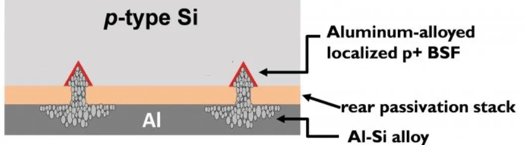
Figure 5 A figure showing the bulk silicon, passivation layer, and aluminum layers in a laser-fired contact material stack. [48]
Although p-type silicon is the dominant starting material for silicon solar cells, researchers have increasingly explored LFCs on n-type silicon as well. This is because the material properties of n-type silicon make it better suited to the cost-effective fabrication of high efficiency cells [49], [50]. In industry, p-type silicon has been favored because the formation an n-type emitter with phosphorous diffusion is relatively simple and doubles as a gettering process that improves material performance by reducing impurity concentrations [12], [51], [52]. In contrast, the formation of a p-type emitter on an n-type substrate requires a high-temperature boron diffusion process that is not optimal for industrial-scale production. LFCs can form local aluminum junctions that serve as p-type emitters, which has led to renewed interest in n-type silicon cells with LFCs [29].
1.2.1 LFC lasing process
The use of lasers in solar cell manufacturing has the potential to significantly improve fabrication throughput and cell efficiency, which are two essential factors in reducing the cost of PV [28]. Already, lasers have been used in industry for edge isolation, surface texturing, selective emitter doping, and wafer dicing [31], [53]–[56]. In comparison with the 13-step photolithography technique shown in Figure 4, laser firing reduces local rear contact formation to two deposition steps for the dielectric and metal stack, then the firing step. This streamlined process holds great
21
promise for the use of local rear contacts in high-efficiency architectures and their industrial success.
In the LFC process, a single laser is used in three stages:
1) Metal melting: the laser selectively heats and melts a spot on the rear aluminum contact layer. The metal melts and the local heat induces thermal and mechanical stress.
2) Dielectric ablation: The stress from the local heat ablates the passivation layer, leaving a hole that exposes the underlying silicon. As the laser heats the exposed silicon, it melts and is thermally expelled out of the hole [10], [53], [57], [58].
3) Metal-silicon alloying and contact formation: The high temperature reached in silicon in contact with aluminum increases the solubility and diffusivity of aluminum in silicon [43]. This facilitates the formation of the silicon-aluminum eutectic upon cooling, which provides an electrically conductive path out of the bulk [10], [32], [59].
The most commonly studied LFC process uses a single laser with 1064 nm wavelength to fire the material stack. Multiple parameters have been tested, including laser defocusing, the number of pulses per contact, and frequencies between 100 Hz and 30 kHz. [31], [32], [44], [57], [60]–[62]).
Damage is the primary concern with the LFC process. The laser process introduces a large amount of energy to a small volume (the affected surface area is on the order of 50 µm2), which results in significant structural damage to the substrate and passivation surrounding the contact. An excess of laser energy can cause defects in the silicon crystalline structure. These defects can act as recombination centers, reducing the number of carriers available for collection and device performance. In processes that use an aluminum contact layer, LFCs incorporate a localized BSF due to the final aluminum-silicon alloy. The BSF improves the recombination dynamics at the LFC, as long as excessive damage has not been caused to the surrounding regions [63].
One way to reduce recombination is to incorporate a dopant layer into the volume underneath the rear silicon-metal contact [56]. By firing through a dopant layer, a high concentration of dopant is incorporated into the molten silicon substrate selectively melted by a laser [64].
22
Because a single laser serves three purposes, the efficiency and quality of the LFC process are restricted. For example, using a laser optimized for dielectric ablation to also alloy aluminum and silicon may result in more damage to the silicon bulk, compared to using separate optimized lasers for ablation and alloying. Considering the varying depths and thicknesses of the material layers and energy doses required to achieve melting, ablation, and alloying, the lasing process and LFC quality could be improved by using multiple lasers with wavelengths and pulse widths optimized for each task.
1.2.2 LFC state of the art
Extensive characterization efforts have led to improvements in LFC processing techniques. LFCs are typically fabricated with nanosecond pulse durations, even though extremely precise and costly control of the process is needed to prevent significant ablation of the aluminum layer. In the last decade, the majority of research groups have studied the laser-firing process with single or multiple nanosecond pulses and wavelengths in the green spectrum. [47], [65]–[67].
In general, results have shown a significant loss of aluminum at high vapor pressures and poor contact between the inner aluminum-silicon eutectic and the metallization on the dielectric passivation [68]–[70]. Since aluminum is needed for the aluminum-silicon alloy to form contact, expulsion of aluminum from the contact area should be avoided. Laser pulses ideally should minimize heating of the aluminum surface, leading to an exploration of lower laser powers and defocused beams [43]. Conversely, millisecond pulse lengths can result in improved melting and mixing of aluminum and silicon, in comparison with shorter wavelength lasers [62]. It is, however, challenging to integrate millisecond lasers into LFC production throughput requirements.
As shown in Figure 6, researchers have explored microsecond pulse durations because they offer the advantage of reduced metal expulsion and can be implemented with diffractive optics to process multiple contacts simultaneously to meet production demands [69]. The longer pulses also enhance the alloying of aluminum and silicon in the contact region and improve the formation of a local BSF, which has been shown to decrease recombination at the contact surface [47], [65].
23
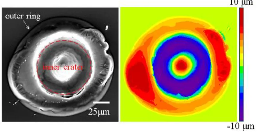
Figure 6 A scanning electron micrograph (SEM) (left) and optical profilometry measurement (right) showing the characteristic inner crater and outer aluminum ring for an LFC fired with a microsecond pulse. [69]
In particular, various parameters using infrared lasers with microsecond pulse durations have been applied and characterized. Such microsecond pulse efforts have correlated aluminum-silicon alloy contact formation with the appearance of a distinct inner crater and outer ring [69]. The regions have been identified as an inner crater where the material first melts under laser irradiation and grows radially with time, based on conductive and convective heat transfer mechanisms. The inner crater is modeled as increasing with fluence. The outer ring region occurs due to the expulsion of aluminum and silicon from the inner crater region [69].
1.2.3 Previous LFC characterization efforts
Thorough understanding of the laser-matter interactions is needed to ensure LFC process control. As a result, LFCs have been extensively characterized since their development in 2002. Multiple research groups have successfully and measured devices with LFCs [29], [44]–[46], [50]. Efficiencies as high as 22.4% have been reported, with efficiencies over 18% that have been repeatedly achieved [30], [71]. Device performance with LFCs have been reported using metrics like open circuit voltage, short circuit current, fill factor, and conversion efficiency [49], [72], [73]. Yet deeper understanding of the contacts require further characterization.
Numerous groups have already studied the property-process relationship between a single laser process and electrical properties, composition, and lifetime degradation [32], [60], [61], [65], [70], [74], [75]. Although advanced characterization methods for laser processing exist, the
24
relationship between laser process, material stack, and electrical performance is still an open research topic in the context of PV. Grohe et al. used laser secondary neutral mass spectroscopy and EBIC measurements to evaluate the feasibility of transferring LFC processing onto the industrial scale [46]. Others have attempted to relate the lasing process to electrical properties to predict process control. Kray and Glunz first demonstrated that the passivation layer of LFCs can significantly reduce SRV, then modeled the SRV of any LFC rear side as a function of base doping and contact pitch [47]. Fischer et al. developed an analytical model to calculate SRV of point-contacted rear side LFCs [76].
From Fischer’s model, Kray and Glunz investigated the relationship between rear-side recombination, contact pitch, and base doping for LFCs [47]. Glunz et al. took co-located SEM and EBIC images on LFCs to correlate regions of strong EBIC signal with areas of electrical contact in the LFC [29]. Sanchez-Aniorte et al. performed energy dispersive spectroscopy (EDS) and I-V measurements of different LFC stack parameters and lasing conditions to identify elemental characteristics of good contact within the parameter space [60]. Urabe et al. characterized the extent of laser damage on the passivated silicon bulk using microwave photoconductance spectroscopy (µ-PCD) for lifetime mapping [77]. Raghavan et al. used cross-sectional transmission electron microscopy (TEM) to relate laser parameters to morphology, resistance, and composition of LFCs [70]. Raghavan et al. later evaluated the influence of changes in microsecond laser processing parameters on contact morphology, resistance, and composition [69]. Glunz et al. tested LFCs on n-type silicon, using the laser to contact and form the emitter. This demonstrated that LFCs result in a local Al-BSF surrounded by a small damaged layer [78]. Schneiderlochner determined that LFC lasing is not causing deep bulk damage is not contributing to post-lasing lifetime degradation [79].
The bulk of characterization efforts have focused on optimization of the single lasing process and understanding how lasing affects performance. Many aspects of LFC processing still require better understanding. A large reason for this is the difficulty of finding experimental techniques that can match the high resolution (sub-10 µm) and sensitivity of the parameters of interest [67], [75]. Recently, studies using µ-Raman and µ-photoluminescence measurements have identified highly-doped regions in LFCs. Roigé et al. was able to correlate these results with conductive-atomic force microscopy measurements to identify the high-conductivity zones in
25
LFCs, providing submicron detail about contact formation [75]. Measurements at these resolutions and higher can elucidate details about the effects of laser processing that have previously been too difficult to access.
1.3 Current challenges to implementing LFC’s in the market
Implementing LFCs for high-efficiency cell architectures requires that LFC processing produces consistent results. This necessitates a full understanding of how lasing affects the structure and properties of a solar cell. Previous characterization efforts described in 1.2.3 Previous
LFC characterization efforts (23-25) have assessed how lasing conditions affect the structure and
electrical properties of LFCs.
Recombination remains a challenge to the application of LFCs to industry because the damage caused by excessive laser energy affects the passivation layers and substrate that surrounds each LFC. This can result in defects that act as recombination centers, where generated carriers are lost and thus unable to contribute to the current [56]. At the eutectic interface with silicon, structural defects due to melted and recrystallized silicon are large contributors [59].
The ongoing research in laser processing parameters reflects continuing difficulties in process optimization. It is difficult to predict damage profiles and lifetime degradation. Laser-firing generally involves an infrared laser, and Molpeceres et al. has reported that the choice of laser can significantly influence the contact quality [55]. The removal of passivation and melting and recrystallization of silicon introduce defect states for free carriers to recombine [31], [43]. Laser damage to the bulk silicon is an unsolved issue that limits overall cell efficiency. This motivates further exploration of the lasing parameter space to understand how to achieve contact with minimal disorder to the silicon and passivation layers.
The state-of-the-art single laser firing process uses the same lasing parameters for melting metal, dielectric ablation, and eutectic formation. Because one laser must serve three purposes, it is not optimized for any of its functions and likely creates more bulk damage than necessary. Ideally, a small-diameter laser should rapidly deposit a high dose of energy to ablate the dielectric and avoid heating the surrounding material unnecessarily. Another larger-diameter, long laser pulse should be used to encourage metal reflow and mixing with the exposed silicon.
26
Using one laser requires a compromise between these functions. Raghavan et al. established that pulse width influences whether ablation or melting occurs [69], [80]. The absorption depth of laser energy depends on the wavelength of light applied. One laser results in a lasing process that deposits excessive energy into the silicon, causing more material to melt and recrystallize than necessary for contact formation. Lifetime-limiting structural defects are the result, and it remains difficult to predict damage profiles and lifetime degradation. Laser-matter interactions need to be related to the LFC performance and their effects on the bulk substrate.
Attempts to optimize lasing parameters have found that specific contact resistances as low as .91 mΩ cm2 for visible lasers and .57 mΩ cm2 for UV lasers could be obtained. The suspected
reason for this is that the UV laser may absorb more shallowly than the visible laser, generating fewer defects [61].
Optimizing lasing parameters is important for reducing overall damage [55], [60], [81]. The ideal laser process would deposit just enough energy to heat the aluminum until mo lten, introduce only enough stress to ablate the dielectric layer, then melt the silicon and alloy it with aluminum for contact formation. With a single laser process, the laser that can achieve dielectric ablation is likely more powerful than needed to melt the bulk silicon, resulting in unnecessary damage. Instead of using one laser for tasks that have power requirements, we have tested a two-laser firing process for LFC formation. The two-two-laser approach could improve over the state-of-the-art because each laser is optimized for a single task (melting vs. ablating), meaning that the minimum energy for each task can be targeted.
1.4 Approach
In my thesis, I hypothesize that a simultaneous two-laser firing process can improve upon the one-laser process by using two task-optimized lasers for dielectric ablation and melting/mixing. The aim is to minimize the amount of energy deposited in the silicon, while achieving eutectic formation. I address the issue of process optimization and LFC characterization by 1) testing a simultaneous two-laser LFC firing process and 2) applying high-sensitivity, synchrotron-based techniques to evaluate elemental constitution LFC on the sub-micron scale and compare these to electrical properties to establish a property-process relationship for different LFC conditions.
Chapter 2 (pgs. 27-31) contains background information about the LFC material stack tested and the structural and electrical characterization techniques. In Chapters
27
3. Experimental Results (pgs. 31-38) and 4 (pgs. 39-43), I apply these characterization
techniques to single-laser and double-laser LFC samples to relate the process to the structural and electrical properties within the chosen parameter space. I also show how synchrotron-based XRF techniques can provide a unique way to characterize the structural properties of LFCs.
The goal is to achieve the same contact quality as a single-laser process, but with less damage. As with a single laser, this two-laser process starts with a 1064 nm microsecond laser that melts the metal surface. As the dielectric is exposed under the molten metal, the 512 nm nanosecond laser is turned on. The 512 nm laser pulses between 35 and 70 times, delivering pulses of energy that introduce thermal stress to ablate the passivation layer. Because the 1064 nm laser is still on, energies can couple so that the 512 nm laser can deposit less energy than in a single-laser process. This minimizes the damage caused below the dielectric. When the dielectric is removed, the 512 nm laser should no longer pulse while the infrared (IR) laser is still on. This IR laser heats the exposed and ideally minimally damaged silicon, as the melted metal reflows into the contact hole for alloying.
2 Methods
2.1 Sample preparation
The processing parameters for this work were chosen from baseline laser energy doses and wavelengths that had been established during previous experiments. For the green laser parameters, the number of pulses per LFC were chosen based on lifetime degradation studies. The pulses per LFC in this work were chosen based on how much lifetime degradation was visible using photoconductance-calibrated photoluminescence, which is a characterization technique discussed in 2.3.1.1 Photoconductance-calibrated Photoluminescence Imaging (PC-PLI) (pg. 30). The IR lasing conditions were picked based on the lowest energy that resulted in observable metal melting in the microscope. The higher IR lasing conditions were chosen to target incremental structural changes caused by the melting.
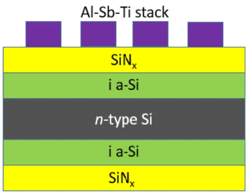
The samples were prepared by the Institute of Energy Conversion (IEC), located at the University of Delaware, and IPG Photonics (IPG). IEC fabricated the material stack, consisting of an aluminum-antimony-titanium metal layer, an intrinsic amorphous silicon layer, a silicon nitride passivation layer, an n-type crystalline silicon layer, then another amorphous and passivation layer, such that the rear is metallized and the front surface is passivated. The material stack is shown in
28
Figure 7. The specific thicknesses of the layers are as follows: 150 µm of n-type Czochralski crystalline silicon, 8 nm of intrinsic amorphous silicon (i a-Si), 60 nm of hydrogenated amorphous silicon nitride (SiNx), and metal strips for LFCs made of 5 nm of titanium, 50 nm of antimony, and
500 nm of aluminum. The titanium layer assists adhesion between the antimony and the silicon nitride passivation layer. The antimony serves as the n-type dopant for the LFC after firing. The thicker layer of aluminum is used for lateral current conduction [82].
Figure 7 The material stack of the samples used to test different LFC lasing parameters. The layers are not to scale.
Polished and textured n-type float zone wafers with 1-5 Ωcm resistivity were used. The textured samples have pyramidal structures of 1-3 µm. Samples were cleaned with Piranha solution (1:30 H2O2:H2SO4) and HF before the amorphous silicon layers and silicon nitride layers
were deposited using plasma-enhanced chemical vapor deposition. Electron beam evaporation was used to deposit the metal stack in strips on the rear side of each sample.
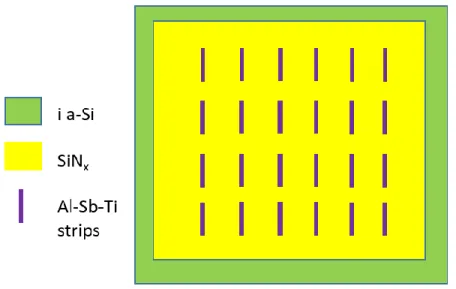
On each sample, four rows and six columns of metallized strips were deposited on the silicon nitride, as shown in Figure 8. Each strip had 5 LFC spots fired on it, with .5 mm spacing. Each row corresponds to a different lasing condition. The lasing conditions were repeated to demonstrate repeatability and to improve accuracy when measuring contact resistance.
29
Figure 8 A diagram showing the rear of the sample. Individual LFC spots were fired into the metallized strips. Each row corresponds to a new lasing condition. The dimensions are not to scale.
2.2 LFC Lasing Parameters
Different combinations of two lasers of different wavelengths were tested. The first laser was a 532 nm (“green”) fiber laser manufactured by IPG Photonics. The pulse width was set at 1 ns and the pulse energy was 2.8 µJ. The green laser fired each spot multiple times, either 35 or 70 times. The beam was defocused to 650 µm. The second laser was a 1070 nm (“IR”) fiber laser also manufactured by IPG Photonics. Two pulse widths, 46 and 50 µs, were used to result in pulse energies of 140 and 400 µJ, respectively. The IR laser was only fired once. The 46 µs (140 µJ) IR lasing parameter was chosen because it was the minimum energy dose at which visible melting of the metal stack was achieved. The parameters are listed in Table 1.
Laser wavelength Pulse width Pulse energy (µJ) Pulses per LFC Energy (µJ)
532 nm (Green) 1 ns 2.8 35 98
1 ns 2.8 70 196
1070 nm (IR) 46 µs 140 1 140
50 µs 400 1 400
30
2.3 Characterization Techniques 2.3.1 Electrical Characterization
2.3.1.1 Photoconductance-calibrated Photoluminescence Imaging (PC-PLI)
Two of the typical methods to measure minority carrier lifetime in silicon employ PCD and photoluminescence (PL). The photoconductance tool used in this work was the Sinton Instruments WCT-120. This measurement system comprises of a flash lamp, a calibrated light sensor, and a radio frequency (RF) coil. A sample is measured by placing it on the RF coil, then using the flash lamp to generate a broadband light source that faces the sample. This flash excites carriers in the sample, and the carriers induce a voltage in the RF coil. The voltage is recorded as a function of time, while the light sensor measures the incident photon flux to determine the injection level. The output data consists of the apparent lifetime across the measured injection range [83].
Photoluminescence (PL) measurements can be performed as a transient measurement or as a quasi-steady-state (QSS) measurement that uses a charge-coupled device (CCD) camera. In the transient approach, carriers are pumped into an excited state. Lifetime is proportional to the intensity of the luminescence signal, which relates to how much radiative recombination is occurring in the material. In the QSS approach, which is commonly used for silicon, the sample is uniformly illuminated with a single wavelength above the bandgap of the material. A CCD camera images luminscent photons in space [84].
With this QSS approach, the measured luminescence intensity must be calibrated to the excess carrier density or lifetime of the material. Photoconductance calibration and self-consistent calibration have both been used to convert luminescence intensity into lifetime values [85], [86]. In QSS-PL, the generation rate across the sample is constant while the measured injection level could vary. Multiple images must be taken at a range of illumination laser powers to specify an injection-dependent lifetime curve.
Contrast was used to evaluate change in sample lifetime after lasing. Over regions with consistent peaks and valleys of PL signal, which correspond to unlased and lased regions, points were selected to measure intensity. Iin indicates the intensity of a spot in the valley that is visibly
within the darkened lased region of lower lifetime. Iout indicates the intensity of an unlased spot,
31 𝐶𝑜𝑛𝑡𝑟𝑎𝑠𝑡 = 𝐼in− 𝐼out
𝐼out
Eq. 4
Here, positive contrast values correspond to lifetime degradation. Photoluminescence is used to evaluate minority carrier lifetime, τeff, such that a lower PL signal corresponds to shorter
lifetimes [84]. Two terms contribute to the value of τeff. One is a bulk lifetime term, τbulk, which
describes the minority carrier lifetime in the bulk of the material. In the bulk, carriers recombine by the mechanisms described in Section
µ-XRF data collection can occur using a step-by-step mode (“stepscans”) or a newly-implemented on-the-fly mode (“flyscans”). With stepscans, the sample must be measured and shifted to collect fluorescence data at each pixel, until a map of pixels is formed. This incremental shifting requires approximately 300 ms per pixel of additional “settling” time. The advantage of flyscans is that the sample continuously moves while the detector continuously collects data. As a result, flyscans avoid the 300 ms per pixel stepscan overhead and enable faster scanning of samples. Given the same stepscan time, flyscans can map larger areas while maintaining the same sensitivity, and can scan an area ten times faster than a stepscan by halving sensitivity [95].
3. Experimental Results
The effect of a two-laser simultaneous process was evaluated before and after processing by observing the structural and electrical characteristics of LFC material stacks after processing.
3.1 PL Images
All PL imaging was performed using the 808 nm diode laser and a Princeton Instruments PIXIS 1024BR camera, which was fitted with an indium phosphide wafer and a Schott RG1000 long-pass filter. The Sinton Instruments WCT-120, an offline wafer-lifetime measurement tool, was used to calibrate the PL images [85]. A Czochralski silicon sample of similar thickness, reflectivity, and resistivity to the LFC samples was used to determine the calibration parameters. The sample thickness was 150 µm, reflectivity was .12, and doping was 3 x 1015 cm-3, based on the QSSPC resistivity estimate of 1.5 Ω-cm2. The setup did not correct for lateral carrier diffusion due to inhomogeneous excess carrier densities, photon scattering or reabsorption within the sample, or photon spreading within the sensor [96]. Without correction, lateral carrier diffusion can affect the spatial information of the measurement.
32
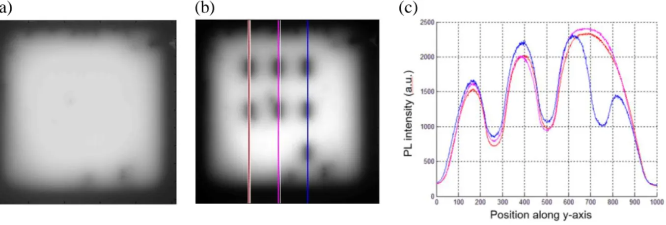
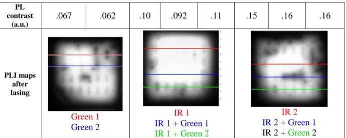
First, the minority carrier lifetime of each sample was measured before laser processing. The lifetimes were taken using the set-up described above, and the sample lifetime was calculated as the average of lifetimes over a 300-pixel circle centered in the image. Laser power percentage was varied between 10% and 60% to find a setting that produced optimal PL images. The images of lased samples in Table 2 were taken with 40% laser power and contrast values were used to evaluate lifetime degradation.
After laser processing, PLI linescans were taken down a column on each sample, as seen in Figure 9 (b). As seen in Figure 9 (c), each linescan plot shows lifetime values as a function of position on either the x- or y-axis. Post-lasing lifetime degradation was evaluated by calculating the contrast between the lased line and the un-processed area around each lased line. Contrast values were calculated in terms of arbitrary units (a.u.) in MATLAB by loading each PL image and the accompanying PL data, manually selecting 30 points within an LFC on a strip, and then selecting 30 points right outside the metal strip. The first 30 points provide lifetime values for laser-degraded material, and the second 30 points provide lifetime values for unprocessed material. For the 30 data pairs, contrast was calculated according to Equation 5. The means of the 30 calculated contrast values are shown for each lasing condition in Table 2.
(a) (b) (c)
Figure 9 PL images of one sample taken (a) before laser processing, (b) after lasing processing with sampled linescans shown in color, and the corresponding plot of PL intensity shown for the linescans.
Group 1 Group 2 Group 3
Lasing
condition Green 1 Green 2 IR 1
Green 1 + IR 1 Green 1 + IR 2 IR 2 Green 2 + IR 1 Green 2 + IR 2 Energy dose (µJ/cm2) 98 196 140 238 336 400 498 596
33 PL contrast (a.u.) .067 .062 .10 .092 .11 .15 .16 .16 PLI maps after lasing Green 1 Green 2 IR 1 IR 1 + Green 1 IR 1 + Green 2 IR 2 IR 2 + Green 1 IR 2 + Green 2
Table 2 Contrast values for different lasing conditions. The groups and condition names refer to those described in Table 1.
3.2 Transmission line measurements of specific contact resistance
RC was measured using TLM. The resistance values are shown in Table 3. For each sample,
five sets of data were used to approximate a linear fit to determine specific contact resistance. The sets of data were taken by measuring the resistance between strips. For example, one set of data measured the resistance between Strip 1 to Strips 2-6, the second set of data measured the resistance between Strip 2 to Strip 1 and Strips 3-6, and so on.
Figure 10 A row of LFC strips that is used for TLM measurements. One data set corresponds to the resistance measurements between one strip and every other strip.
For the samples only fired with a “green” laser, no ohmic contact was measureable between any of the strips. The standard error, 1.5 mΩ cm2, was approximately the same for the non-infinite
RC measurements. The measured RC and length between the two measured LFC strips were entered
into Microsoft Excel, then the “STEYX” function was used to calculate the error of the linear regression. Lasing condition Green 1 Green 2 IR 1 Green 1 + IR 1 Green 2 + IR 1 IR 2 Green 1 + IR 2 Green 2 + IR 2
34 Energy dose (µJ/cm2) 98 196 140 238 498 400 336 596 RC (mΩcm2) ∞ ∞ <13.5 ± .73 <6.7 ± .73 <8.7 ± .73 <8.9 ± .73 <8.5 ± .73 <6.8 ± .73 Table 3 RC for different lasing conditions as measured by TLM. The condition names refer to those
described in Table 1. Standard error for all non-infinite RC measurements was approximately .73
mΩ cm2.
3.3 µ-X-ray fluorescence spectroscopy for elemental mapping
After lasing, spatially-resolved µ-XRF measurements were taken of a single LFC for each condition. The flyscan mode allowed us to determine elemental composition with unprecedented levels of sensitivity, resolution, and speed. All elemental channel maps and the Si:Al map are shown in Table 4. The scale bar indicating elemental counts is in log10, so 15 actually indicates
35
Phase 1 Phase 2 Phase 3
Lasing
condition Green 1 Green 2 IR 1 Green 1 + IR 1 Green 2 + IR 1 IR 2 Green 2 + IR 2 Green 2 + IR 2 Energy dose (µJ/cm2) 98 196 140 238 336 400 498 596
µ-XRF maps (all scale bars in log10)
Si:Al
Silicon
Aluminum
Antimony
Titanium
Table 4 µ-XRF maps showing counts for silicon, aluminum, antimony, titanium, and Si:Al for LFCs fired with the described lasing conditions.
36
All silicon maps contain a smear to the left of the image. This is an artifact caused by the incident X-ray beam hitting the sample at an angle. Since the silicon channel was used to calculate Si:Al, some Si:Al maps also contain the artificial smear.
In general, the ROIs show aluminum, titanium, and antimony counts outside a large central hole and predominantly silicon counts within the hole. To facilitate discussion of the LFCs, three contact formation phases have been defined for comparison. As first described in 2.2 LFC Lasing Parameters, Group 1 refers to the two smallest LFCs that are formed using “Green 1” and “Green 2” lasing conditions. Group 2 refers to three LFCs that use the 140 µJ IR pulse: “IR 1,” “Green 1 + IR 1,” and “Green 2 + IR 1”. Group 3 refers to the three largest LFCs that use the 400 µJ IR pulse: “IR 2,” “Green 1 + IR 2,” and “Green 2 + IR 2.”
For Group 1, “Green 1” shows silicon counts. With the scales used, “Green 1” does not show significant elemental differences between un-lased and lased regions. The “Green 2” map shows higher metal counts in a ring surrounding a high-silicon count hole. For Group 2, the samples show rings of high metal counts and a cavity that is high in silicon counts only. For Group 3, three distinct features of each LFC are visible. There is an outer ring with a splatter pattern that contains high metal counts. Within the outer ring, there is another ring that is most apparent in the titanium channel. Lastly, the central hole is metal-poor and silicon-rich.
MATLAB was used to define an area in each Si:Al map and calculate the average Si:Al value within a uniform section of the LFC. These average Si:Al values are shown in Table 5.
Phase 1 Phase 2 Phase 3
Lasing
condition Green 1 Green 2 IR 1
Green 1 + IR 1 Green 2 + IR 1 IR 2 Green 2 + IR 2 Green 2 + IR 2 Energy dose (µJ/cm2) 98 196 140 238 336 400 498 596 Si:Al 1.01 13.4 24.5 23.0 29.1 55.1 63.8 61.9
Table 5 The Si:Al values for each of the lasing conditions, as determined from the µ-XRF maps 3.4 SEM and EDS
SEM images were taken for each processing condition to evaluate the structural characteristics of the LFC. The same LFC was used for the EDS and µ-XRF studies to correlate elemental and structural features.
37
Phase 1 Phase 2 Phase 3
Lasing
condition Green 1 Green 2 IR 1
Green 1 + IR 1 Green 2 + IR 1 IR 2 Green 2 + IR 2 Green 2 + IR 2 Energy dose (µJ/cm2) 98 196 140 238 336 400 498 596 SEM images
Table 6 SEM images showing contacts that were fired with each lasing condition.
The SEM images are shown in Table 6. In Phase 1, the “Green 1” condition resulted in a solid formation with small splatter features at the edge. “Green 2” appears similar to Green 1, but with larger splatter features and surrounding droplets. In Phase 2, the rings seen in the XRF maps are also visible in the SEM images. The two conditions that include Green pulses include a spot in the center of the contact. In Phase 3, all contacts show a ring with splatters extending outward. The “IR 2” condition has an amorphous interior, in comparison to the “Green 1 + IR 2” and “Green 2 + IR 2” conditions that exhibit small craters and pool-like formations
EDS was taken for “IR 2” sample to examine its elemental distribution. Higher color saturation indicates greater elemental counts, while black indicates that the element was not detected.
4. Discussion
The aim of this work is to characterize the principal differences between single-shot and double-shot lasing processes and to determine how each process can improve LFC quality. An ideal LFC should include at least (1) a metal-silicon interface for low RC and (2) a small lased
contact area to minimize recombination and minority carrier lifetime degradation [97].
In this section, the experimental results presented in Chapter 3 (pgs. 31-38) are correlated to identify relationships between the lasing process and LFC properties, like the metal-silicon interface and the lifetime characteristics listed above. The unique combination of lifetime information from PC-PLI, elemental mapping using µ-XRF, RC values from TLM, and
micrographs from SEM combine structural and electrical properties that can be related to the range of tested processes. Characterization of the double-shot lasing processes, which have not been
38
tested in literature before, provides insight into whether LFC production can be optimized. With the sensitivity and resolution of the µ-XRF maps, the microstructure of LFCs can be studied at an unprecedented level for both single- and double-shot lasing processes.
The results in this work pertain to a sample set of six conditions, where each condition is a unique lasing process. With these six conditions, a comparison was possible between single-lasing conditions, which include “Green only,” “IR only,” simultaneous double-lasing conditions, which include “Green + IR.” For these conditions, the impact of increasing the green and/or IR condition on structure, electrical properties, and lasing process was observed. These results suggest that a “Green + IR” process could possibly produce a superior LFC to single lasing conditions, but cannot conclude what conditions are optimal. Ideally, a parameter sweep of both the “Green” and “IR” lasing conditions would have been conducted to determine the result of incremental process change. A parameter sweep would also provide further evidence to confirm the structure-property-process relationships that these results suggest.
Furthermore, the RC TLM data have represent upper bounds, and were repeatable only for
textured samples, but not for polished samples. RC is one of the determining factors of an effective
LFC, which limits the conclusions that can be drawn about structure-property-process relationships.
The data is presented in the same groups (Group 1, Groups 2, Group 3) described in 3.1
PL Images (pg. 31) and addressed as two optimization problems.
1) LFC process optimization in 4.1, by examining single-shot and double-shot lasing 2) LFC characterization optimization in 4.2, by using µ-XRF as a tool for evaluating LFCs
(via the Si:Al ratio, as an indicator of contact formation)
To discuss process optimization, the lasing process will first be reviewed to emphasize the goal of the experiment. In section 4.1, the structure-property-process relationships will be discussed, beginning with how the lasing process impacts lifetime degradation (PLI data) in 4.1.1,
RC in 4.1.2, and elemental distribution in 4.1.3. In 4.1.4, these results are summarized and
suggestions are made about how to improve LFC processing. To discuss LFC characterization in sub-section 4.2, the EDS data and u-XRF data are compared to show that u-XRF may provide an alternate quantitative measure of contact quality.
![Figure 3 An image of the cross-section of the rear aluminum contact and the eutectic layers in an Al-BSF cell [10]](https://thumb-eu.123doks.com/thumbv2/123doknet/14499706.527605/17.918.114.657.121.269/figure-image-cross-section-aluminum-contact-eutectic-layers.webp)
![Figure 4 A comparison of the LFC process and the localized contacting process for point contact patterning on passivated rear silicon solar cells [30]](https://thumb-eu.123doks.com/thumbv2/123doknet/14499706.527605/19.918.184.791.147.433/figure-comparison-process-localized-contacting-process-patterning-passivated.webp)